EP1458033A2 - Composant semi-conducteur de protection, dispositif semi-conducteur le comprenant et procédés de fabrication correspondants - Google Patents
Composant semi-conducteur de protection, dispositif semi-conducteur le comprenant et procédés de fabrication correspondants Download PDFInfo
- Publication number
- EP1458033A2 EP1458033A2 EP04005858A EP04005858A EP1458033A2 EP 1458033 A2 EP1458033 A2 EP 1458033A2 EP 04005858 A EP04005858 A EP 04005858A EP 04005858 A EP04005858 A EP 04005858A EP 1458033 A2 EP1458033 A2 EP 1458033A2
- Authority
- EP
- European Patent Office
- Prior art keywords
- region
- exposed
- semiconductor
- protection element
- silicide layers
- Prior art date
- Legal status (The legal status is an assumption and is not a legal conclusion. Google has not performed a legal analysis and makes no representation as to the accuracy of the status listed.)
- Withdrawn
Links
Images






Classifications
-
- H—ELECTRICITY
- H10—SEMICONDUCTOR DEVICES; ELECTRIC SOLID-STATE DEVICES NOT OTHERWISE PROVIDED FOR
- H10D—INORGANIC ELECTRIC SEMICONDUCTOR DEVICES
- H10D1/00—Resistors, capacitors or inductors
- H10D1/40—Resistors
- H10D1/43—Resistors having PN junctions
-
- D—TEXTILES; PAPER
- D05—SEWING; EMBROIDERING; TUFTING
- D05B—SEWING
- D05B3/00—Sewing apparatus or machines with mechanism for lateral movement of the needle or the work or both for making ornamental pattern seams, for sewing buttonholes, for reinforcing openings or for fastening articles, e.g. buttons, by sewing
- D05B3/02—Sewing apparatus or machines with mechanism for lateral movement of the needle or the work or both for making ornamental pattern seams, for sewing buttonholes, for reinforcing openings or for fastening articles, e.g. buttons, by sewing with mechanisms for needle-bar movement
- D05B3/025—Sewing apparatus or machines with mechanism for lateral movement of the needle or the work or both for making ornamental pattern seams, for sewing buttonholes, for reinforcing openings or for fastening articles, e.g. buttons, by sewing with mechanisms for needle-bar movement with a pair of needles mounted on the needle-bar
-
- D—TEXTILES; PAPER
- D05—SEWING; EMBROIDERING; TUFTING
- D05B—SEWING
- D05B55/00—Needle holders; Needle bars
- D05B55/14—Needle-bar drives
-
- H—ELECTRICITY
- H10—SEMICONDUCTOR DEVICES; ELECTRIC SOLID-STATE DEVICES NOT OTHERWISE PROVIDED FOR
- H10D—INORGANIC ELECTRIC SEMICONDUCTOR DEVICES
- H10D89/00—Aspects of integrated devices not covered by groups H10D84/00 - H10D88/00
- H10D89/60—Integrated devices comprising arrangements for electrical or thermal protection, e.g. protection circuits against electrostatic discharge [ESD]
- H10D89/601—Integrated devices comprising arrangements for electrical or thermal protection, e.g. protection circuits against electrostatic discharge [ESD] for devices having insulated gate electrodes, e.g. for IGFETs or IGBTs
- H10D89/811—Integrated devices comprising arrangements for electrical or thermal protection, e.g. protection circuits against electrostatic discharge [ESD] for devices having insulated gate electrodes, e.g. for IGFETs or IGBTs using FETs as protective elements
Definitions
- the present invention relates to a semiconductor protection element, a semiconductor device and a method for manufacturing the same, and more particularly to the semiconductor protection element and the semiconductor device in which an electrostatic protection circuit to protect the semiconductor protection element or the semiconductor device from electrostatic discharge (ESD) is formed therein and the method for manufacturing the same.
- ESD electrostatic discharge
- the impurity diffusion layer having a shallow depth causes resistance values in the source region and drain region to become high and the current driving capability of a transistor to be deteriorated remarkably.
- a transistor which has a structure in which a silicide layer is selectively formed in a source region and a drain region to lower a resistance value on the source region and drain region.
- Such the structure is generally called as a salicide structure.
- the salicide has a problem in that, though it is possible to lower a resistance value in the source region and in the drain region, it is vulnerable to electrostatic discharge (ESD) .
- ESD electrostatic discharge
- the above condition (2) becomes a big problem.
- the resistance of the protecting element to electrostatic discharge (ESD) is determined depending on distribution of resistance values from a drain to a source. If there exists a local region in which a resistance value is large compared with other region, heat is locally generated in the region, which causes high probability of occurrence of an electrostatic breakdown.
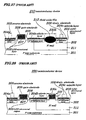
- Figure 26 shows a first conventional example of a semiconductor device 200 disclosed in Japanese Patent No. 2773220 which corresponds to Japanese Patent Application Laid-open No. 20271673.
- the semiconductor device 200 includes a 2-type substrate 201 on which an N + diffusion layer 202 and an LDD-structured layer 203 of impurity concentration being lower than that in the N + diffusion layer 202 in a manner that the two layers overlap each other are formed.
- a first silicide layer 204a On the N + diffusion layer 202 are formed, in a selective manner, a first silicide layer 204a, a second silicide layer 204b, and a third silicide layer 204c. On the first silicide layer 204a is formed a source electrode 205 and on the third silicide layer 204c is formed a drain electrode 206.
- FIG. 27 is a cross-sectional view of a semiconductor device 210, shown as a second conventional example, disclosed in U.S. Patent No. 6479870.
- the semiconductor device 210 shown in Fig. 27 differs from that shown in Fig. 26 in that an N-type well 211 is formed on a surface of a P-type substrate 201 between a second silicide layer 204b and a third silicide layer 204c and in that a field oxide film 212, instead of an LDD-structured layer 203 and an N + diffusion layer 202, is formed between the second silicide layer 204 and the third silicide layer 204c.
- Figure 28 is a cross-sectional view of a semiconductor device 220, shown as a third conventional example, disclosed in U.S. Patent No. 5637902.
- the semiconductor device 220 shown in Fig. 27 differs from that shown in Fig. 26 in that an N-type well 221 is formed on a surface of a P-type substrate 201 between a second silicide layer 204b and a third silicide layer 204c and in that a gate electrode structure 222 made up of a gate oxide film, gate electrode, and a side wall, instead of an LDD-structured layer 203 and N + diffusion layer 202, is formed the second silicide layer 204b and the third silicide layer 204c.
- the semiconductor devices 200, 210, and 220 shown, respectively, in Figs. 26, 27, and 28 have regions 230a, 230b, and 230c in each of which a silicide layer is not formed, respectively, between the second silicide layer 204b and third silicide layer 204c.
- regions 230a, 230b, and 230c with no silicide layer being formed, it is made possible to make uniform resistance existing between a wiring material (not shown) to an end of each of the source electrode and the drain electrode, which enables resistance to electrostatic discharge (ESD) to be increased.
- ESD electrostatic discharge
- the regions such as the N-type wells 211 and 221, or the LDD-structured layer 203 in which the impurity of low concentration is implanted function as regions having a high resistance value.
- the resistor element is made up of regions having high resistance as in the case of the semiconductor device 210 shown in Fig. 27 and the semiconductor device 220 shown in Fig. 28, unlike in the case of the semiconductor device 220 shown in Fig. 28, it is made possible to reduce the area of the semiconductor device.
- ESD electrostatic discharge
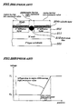
- Figure 29A is a cross-sectional view showing the field oxide film 212 and regions surrounding the field oxide film 212 making up the semiconductor device 210 shown in Fig. 27.
- Figure 29B is a graph showing a relation between a position corresponding to the region shown in Fig. 29A and a voltage to be applied.
- a large current flows due to application of electrostatic discharge (ESD)
- ESD electrostatic discharge
- a rapid voltage drop from V1 to V2 occurs in the region 230b having a high resistance value.
- heat is locally generated in the region 230b having a high resistance value in a concentrated manner.
- the region 230b having high resistance values is formed so as to have a small area and, therefore, an amount of heat generated per unit area becomes very large. Therefore, a probability that the resistor element itself is thermally broken down becomes very large.
- ESD electrostatic discharge
- a semiconductor protection element including:
- both the region having a high resistance value and the region having an intermediate resistance value are exposed on a surface of the semiconductor substrate. Therefore, a resistance value of a semiconductor protection element changes in stages depending on a position and no concentration of heat generation in the region having a high resistance value occurs. As a result, resistance to electrostatic breakdown can be increased when compared with the case of the conventional semiconductor protection element in which a resistor element is formed by using the region having a high resistance value.
- the resistor element is made up of_three kinds of resistance regions including the region having a high resistance value, regions having an intermediate resistance value and regions having a low resistance value and, therefore, a desired resistance can be obtained even in a smaller area and an entire area of a semiconductor protection element can be reduced when compared with the case of the semiconductor protection element in which_the resistor element is made up of the region having a low resistance value or an intermediate resistance value.
- the resistor element or electrostatic protection circuit though having a small area, can have a high resistance to electrostatic breakdown.
- a semiconductor protection element including:
- a semiconductor protection element including:
- a preferable mode is one wherein a field oxide film is formed on the first surface region or on the first exposed region.
- a preferable mode is one wherein the first region is made up of a well region.
- a preferable mode is one wherein the first region is formed on a surface of the semiconductor substrate and in a manner that the first region and the second region are overlapped on a surface of the semiconductor substrate.
- a preferable mode is one wherein, the first impurity concentration of the first region, when it is assumed that a well region is formed on the semiconductor substrate, is higher than that of the well region.
- a preferable mode is one wherein a gate electrode structure is formed on the first surface region or on the first exposed region.
- a preferable mode is one wherein the second exposed region has a surface length being equal to or larger than that of the first exposed region.
- a preferable mode is one wherein a surface length of the second exposed region is equal to or larger than a depth of the second region.
- a semiconductor protection element including:
- a method for manufacturing a semiconductor protection element including:
- a method for manufacturing a semiconductor protection element including:
- a preferable mode is one wherein each of the second regions and the first region are overlapped each other on a surface of the semiconductor substrate.
- a preferable mode is one wherein, the first impurity concentration of the first region, when it is assumed that a well region is formed on the semiconductor substrate, is higher than that of the well region.
- a preferable mode is one wherein the second exposed region has a surface length being equal to or larger than that of the first exposed region.
- a preferable mode is one wherein a surface length of the second exposed region is equal to or larger than a depth of the second region.
- a semiconductor device including:
- a semiconductor device including:
- a semiconductor device including:
- a preferable mode is one wherein a field oxide film is formed on the first surface region or the first exposed region.
- a preferable mode is one wherein a gate electrode structure is formed on the first surface region or the first exposed region.
- a preferable mode is one wherein the second exposed region has a surface length being equal to or larger than that of the first exposed region.
- a preferable mode is one wherein a surface length of the second exposed region is equal to or larger than a depth of the second region.
- a method for manufacturing a semiconductor device including:
- a method for manufacturing a semiconductor device including:
- a method for manufacturing a semiconductor device including:
- a preferable mode is one wherein the second region are formed on a surface of the semiconductor substrate in a manner that the second region and the first region are overlapped.
- a preferable mode is one wherein, the first impurity concentration of the first region, when it is assumed that a well region is formed on the semiconductor substrate, is higher than that of the well region.
- a preferable mode is one wherein a surface length of the second exposed region is equal to or larger than a depth of the second region.
- a preferable mode is one wherein a surface length of the second exposed region is equal to or larger than a depth of the second region.
- a preferable mode is one that wherein further includes a step of forming a field oxide film formed on the first surface region or the first exposed region.
- a preferable mode is one that wherein further includes a step of forming a gate electrode structure on the first surface region or on the first exposed region.
- a resistance value of a semiconductor protection element changes in stages depending on a position and, as a result, no concentration of heat generation in a region having a high resistance value occurs.
- resistance to electrostatic breakdown can be increased.
- the resistor element is made up of three kinds of resistance regions including a region having a high resistance value (exposed region), regions each having an intermediate value (second exposed region) and regions each having a low resistance value and, therefore, a desired resistance value can be achieved in a smaller area compared with the semiconductor protection element in which the resistor element is made up of regions having a low resistance value and regions each having an intermediate resistance value and an area of an entire semiconductor protection element can be made smaller.
- the resistor element or electrostatic protection circuit having a high resistance to electrostatic discharge (ESD) can be formed even in a smaller region.
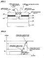
- Figure 1 is a cross-sectional view showing a semiconductor protection element 10 according to a first embodiment of the present invention.
- the semiconductor protection element 10 includes a P-type semiconductor substrate 11 and silicide layers 12 formed on the P-type semiconductor substrate 11.
- an N-type well 13 serving as a first region having a first impurity concentration being a relative low concentration and a pair of N + diffusion layers 14, 14 each serving as a second region having a second impurity concentration being higher than the first impurity concentration of the N-type well 13.
- the N-type well 13, serving as the first region has a first surface region being not covered with the silicide layers 12, and also the two N + diffusion layers 14, 14, serving as the second region, has a second surface region being not covered with the silicide layers 12.
- the first surface region on the N-type well 13 is formed as a first exposed region 13R being exposed on a surface of the P-type semiconductor substrate 11 and the two second surface regions on the N + diffusion layers 14 are formed as second exposed regions 14R being exposed on the surface of the P-type semiconductor substrate 11, in such a manner to surround / sandwich the first exposed region 13R.
- Each of the silicide layers 12 is formed on each of the two N + diffusion layers 14 serving as the second region in a manner that part of each of the two N + diffusion layers 14 makes up each of the second exposed regions 14R each being exposed successively so as to be in contact with the first exposed region 13R.
- first impurity concentration of the N-type well 13
- second impurity concentration of the N + diffusion layer 14
- First impurity concentration 1X10 13 to 2X10 13 (cm -2 )
- Second impurity concentration 1X10 15 to 6X10 15 (cm -2 )
- the first exposed region 13R and second exposed regions 14R are so formed that all the length (hereinafter may be referred to as surface length) 2W of the second exposed region 14R on a surface of the P-type semiconductor substrate 11 is not shorter than a length S (surface length) of the first exposed region 13R on a surface of the P-type semiconductor substrate 11. That is, the surface lengths 2W of the second exposed regions 14R are almost equal to the surface length S of the first exposed region 13R, or the surface lengths 2W of the second exposed regions 14R are longer than the surface length S of the first exposed region 13R. That is, 2W ⁇ S or 2W > S.
- heat is generated in the region 230b having a high resistance value. If a length of the region 230b having a high resistance value is defined as "S”, a length of the heat generated region is expressed as "S".
- regions in which heat is generated are the second exposed regions (each having an intermediate resistance value) 14R and the first exposed region (region having a high resistance value) 13R. That is, a length of the heat generated region is (2W + S). Therefore, by making setting so that the length 2W of the second exposed regions (region having an intermediate resistance value) is almost equal to or more than the length S of the first exposed region (region having a high resistance value) 13R, the expression that 2w + S ⁇ 2S or 2W + S > 2S can be satisfied. As a result, an area of the heat generated region can be doubled compared with that employed conventionally.
- the surface length W of each of the second exposed regions 14R is formed so as to be equal to a depth D of the N + diffusion layer 14 or so as to be larger than the depth D. That is, W ⁇ D.
- Figure 3A is a diagrammatic sketch showing a length L1' of a current path in the conventional semiconductor protection element (making up the semiconductor device 210) and Figure 3B is a diagrammatic sketch showing a length L2' of a current path in the semiconductor protection element 10 according to the first embodiment of the present invention.
- L2' 2 x (W 2 + D 2 ) 1/2
- the semiconductor protection element 10 according to the first embodiment can acquire only the resistance value being equal to that obtained in the conventional semiconductor protection element.
- the length of the path of currents flowing through the N + diffusion layer 14 can be made longer than that employed in the conventional semiconductor protection element and, therefore, the breakdown resistance being larger than that obtained in the conventional semiconductor protection element can be obtained.
- each of the silicide layers 12 serves as a region having a low resistance value
- each of the second exposed regions 14R in each of the N + diffusion layers 14 as a region having an intermediate resistance value
- the first exposed region 13R in the N-type well 13 as a region having a high resistance value.
- Figure 2 is a graph showing relations among positions illustrated in the cross-sectional view of the semiconductor protection element 10 of the first embodiment in Fig. 1 and voltages to be applied to each of the positions, which corresponds to the graph showing the same relation in the conventional semiconductor protection elementin Fig. 29B.
- a voltage drop occurs in the second exposed regions 14R serving as the region having an intermediate resistance value and in the first exposed region 13R serving as the region having a high resistance value.
- a gradient in a voltage drop is constant, while, in the graph shown in Fig. 2, a gradient 81 in a voltage drop in each of the second exposed regions 14R serving as the region having an intermediate resistance value is different from a gradient ⁇ 2 in a voltage drop in each of the first exposed region 13R having a high resistance value. More particularly, the gradient ⁇ 1 in the voltage drop in each of the second exposed regions 14R serving as the region having an intermediate resistance value is smaller than the gradient ⁇ 2 in the voltage drop in each of the first exposed region 13R having a high resistance value.
- the region in which heat generation occurs as the result of the voltage drop from V1 to V2 in the semiconductor protection element 10 is wider than the region in which heat generation occurs as the result of the voltage drop from V1 to V2 in the conventional semiconductor protection element.
- the length of the region in which heat is generated in the conventional semiconductor protection element is L1 and the length of the region in which heat is generated in the semiconductor protection element 10 of the first embodiment is L2 and, since the gradient ⁇ 1 of the resistance region is different from the gradient ⁇ 2 of the resistance region, the length L2 is longer than the length L1.
- the regions having an intermediate resistance value are formed in a place surrounding the region having a high resistance value (first exposed region or first surface region 13R) and the regions having a low resistance value (silicide layer 12) in a place surrounding the regions having an intermediate resistance value (second exposed regions or second surface regions 14R). Therefore, a resistance value of the semiconductor protection element 10 according to the first embodiment changes in stages depending on each of positions within the semiconductor protection element 10 and no concentration of heat generation occurs in the region having a high resistance value (first exposed region 13R or first surface region 13R) .
- resistance to electrostatic discharge (ESD) can be increased.
- the resistor element is made up of three kinds of resistance regions including the region having a high resistance value (first exposed region or first surface region 13R), regions having an intermediate resistance value (second exposed regions or second surface regions 14R) , and the regions (silicide layers 12) having a low resistance value, unlike in the case of the semiconductor protection element employing resistor elements made up of only regions having a low resistance value or regions having an intermediate resistance value, it is made possible to obtain a desired resistance value even in a smaller region which enables an entire area of the semiconductor protection element to be smaller.
- the resistor element or electrostatic protection circuit having a high resistance to electrostatic discharge (ESD) can be formed even in a smaller area.
- a curve A1 shows a snap-back characteristic of a protection element having no drain resistance value
- a curve A2 shows a snap-back characteristic of a semiconductor protection element being employed in the conventional semiconductor device 210
- a curve A3 shows a snap-back characteristic of a semiconductor protection element 10 being employed in the semiconductor device 110 according to the first embodiment, in which a current [A] is plotted as ordinate and a drain voltage [V] as abscissa.
- Figure 4B shows an equivalent circuit diagram of a semiconductor device containing the semiconductor protection element.
- the protection element is made up of a MOS (Metal Oxide Semiconductor) transistor.
- a slop of a characteristic curve occurring after the snap-back operation is determined according to a resistance value appearing when the parasitic bipolar transistor Tr is turned ON and to a resistance value of a drain.
- the curve A1 in Fig. 4A is the characteristic curve obtained when the drain has no resistance and, therefore, the slope of the curve A1 is steep. However, the slopes of the curve A2 and curve A3, since the resistor is connected to the drain, are comparatively gentle.
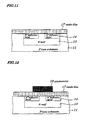
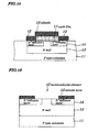
- Figures 5 to 16 are cross-sectional views illustrating manufacturing processes of the semiconductor protection element 10 of the first embodiment.
- FIGs. 5 to 16 one example of the manufacturing method of the semiconductor protection element 10 of the first embodiment is described below.
- a photoresist 15 having a specified pattern is formed on a surface of the P-type semiconductor substrate 11.
- an N-type well 13 serving as a first region of first impurity concentration is formed.
- a photoresist 16 having a pattern used to form N + diffusion layers 14 serving as a second region is formed on a surface of the P-type semiconductor substrate 11.
- N + diffusion layers 14 serving as a second region having an impurity concentration being higher than the first impurity concentration are formed in the N-type well 13.
- the photoresist 16 on the P-type semiconductor substrate 11 is removed.
- the N-type well 13 has a first exposed region (or first surface region) 13R being exposed on a surface of the P-type semiconductor substrate 11 and being formed so as to be sandwiched by two N + diffusion layers 14.
- a silicon oxide film 17 is formed on an overall surface of the P-type semiconductor substrate 11.
- a photoresist 18 having a pattern used to form the first exposed region (or the first surface region) 13R and the second exposed regions (or the second surface region) 14R are formed on the silicon oxide film 17.
- the silicon oxide film 17 is etched using the photoresist 18 as a mask.
- a metal film is deposited on an entire surface of the P-type semiconductor substrate 11 and the silicon oxide film 17 by a sputtering method. After this, by performing heat treatment, the metal film on the P-type semiconductor substrate 11 and the silicon oxide film 17 reacts with silicon to form a silicide layer 12.
- the silicon oxide film 17 and the silicide layer 12 on the silicon oxide film 17 are removed by an etching process.
- the metal film on the silicon oxide film 17 is removed by a chemical reaction at a time of an etching process, since the silicide layer 12 produced by reaction between metal and silicon cannot be removed by etching easily and only the silicide layer 12 on the P-type semiconductor substrate 11 stays.
- the semiconductor protection element 10 of the first embodiment shown in Fig. 1 is formed by processes described above.
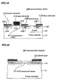
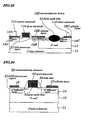
- Figure 17 is a cross-sectional view showing a semiconductor device 110 having a semiconductor protection element 10 of the first embodiment. Moreover, in Fig. 17, same reference numbers are assigned to components having the same function as those in the semiconductor protection element 10 in Fig. 1.
- a first N + diffusion layer 14A, second N + diffusion layer 14B, and third N + diffusion layer 14C are formed on the P-type semiconductor substrate 11 and a first silicide layer 12A is formed on the first N + diffusion layer 14A, a second silicide layer 12B on the second N + diffusion layer 14B, and a third silicide layer 12C on the third N + diffusion layer 14C.
- the semiconductor device 110 shown in Fig. 17 is made up of the P-type semiconductor substrate 11, N-type well 13, second N + diffusion layer 14B and third N + diffusion layer 14C (these two N + diffusion layers 14B and 14C correspond to the N + diffusion layer 14 shown in Figs. 5 to 16), second silicide layer 12B and third silicide layer 12C (these two silicide layers 12B and 12C correspond to the silicide layer 12 shown in Figs. 5 to 16).
- the first silicide layer 12A covers an entire surface of the first N + diffusion layer 14A.
- a source electrode 111 is formed on the first silicide layer 12A and a drain electrode 112 is formed on the third silicide layer 12C.
- a gate electrode structure is provided in which a gate insulating film 113 is formed on the P-type semiconductor substrate 11 between the first silicide layer 12A and the second silicide layer 12B, a gate electrode 114 is formed on the gate insulating film 113, and a side wall 115 is formed in a place surrounding the gate insulating film 113 and gate electrode 114.
- an LDD-structured region 116 is formed.
- the semiconductor device 110 since it has the structure of the semiconductor protection element 10 of the first embodiment, has effects provided by the semiconductor protection element 10 of the first embodiment. That is, in the semiconductor device 110, since the semiconductor protection element 10 has three kinds of resistance regions in a mixed manner, a resistor element or an electrostatic protection circuit having a high resistance to electrostatic discharge (ESD) is formed even in a smaller area.
- ESD electrostatic discharge
- the N-type well 13 is formed on the P-type semiconductor substrate 11 by the same processes as those shown in Figs. 5 to 7.
- the gate insulating film 113 and gate electrode 114 are formed on the P-type semiconductor substrate 11 by photolithography and dry etching.
- an N-type impurity is implanted into the P-type semiconductor substrate 11 to form the LDD-structured region 116.
- the side wall 115 is formed in a place surrounding the gate insulating film 113 and the gate electrode 114.
- the first, second and third N + diffusion layers 14A, 14B, and 14C are formed by the same processes as shown in Figs. 8 to 10.
- the gate electrode 114 and side wall 115 are used as a mask.
- the first, second and third silicide layers 12A, 12B, and 12C are formed, respectively, on the first, second, and third N + diffusion layers 14A, 14B, and 14C by the same processes as shown in Figs. 11 to 16.
- the gate electrode 114 and side wall 115 are used as a mask.
- the source electrode 111 is formed on the first silicide layer 12A and the drain electrode 112 is formed on the third silicide layer 12C.
- the semiconductor device 110 shown in Fig. 17 is formed.
- the semiconductor protection element 10 is constructed using an N channel MOS transistor, however, by changing a conductive type of each of the substrate 11 and other components, the semiconductor protection element 10 according to the embodiment can be configured using a P channel MOS transistor.
- the semiconductor protection element 10 of the first embodiment is constructed as an element on the P-type semiconductor substrate, however, it can be also constructed as an element on the N-type semiconductor substrate or an SOI (Silicon On Insulator).
- Figure 18 is a cross-sectional view showing a semiconductor protection element 20 of the second embodiment of the present invention.
- Configurations in a first region of the semiconductor protection element 20 of the second embodiment differ from those in the first region of the semiconductor protection element 10 shown in the first embodiment in Fig. 1.
- the first region is made up of the N-type well 13 only.
- the first region is made up of an N-type well 13 and an LDD-structured region 21, serving as a third region, formed in a manner that the LDD-structured region and the N-type well are overlapped each other.
- Concentration of an impurity in the LDD-structured region 21 serving as the third region is higher than that in the N-type well 13 and lower than that in the N + diffusion layer 14. Therefore, the first exposed region 13R making up a region having a high resistance value is made up of the LDD-structured region 21.
- the LDD-structured region 21, N-type well 13, and N + diffusion layer 14 are overlapped one another.
- the concentration of the impurity in the LDD-structured region 21 is, for example, 4x10 13 (cm -2 ) to 4x10 14 (cm -2 ).
- the structure of the semiconductor protection element 20 of the second embodiment is the same as the semiconductor protection element 10 of the first embodiment except that structures in their first regions are different from each other.
- same reference numbers are assigned to components having the same function as those in the semiconductor protection element 10 in Fig. 1.
- the concentration of the impurity in the N-type well 13 is compared with that in the LDD-structured region 21, the concentration of the impurity in the LDD-structured region 21 is generally larger than that in the N-type well 13. Therefore, a resistance value per unit length in the LDD-structured region 21 is smaller than that in the N-type well 13, an occupied area of the LDD-structured region 21 is larger than that of the N-type well 13 and a potential gradient in the LDD-structured region 21 is smaller than that in the N-type well 13.
- the semiconductor protection element 20 of the second embodiment since the structure of the LDD-structured region 21 is added to that of the semiconductor protection element 10 of the first embodiment, larger resistance to electrostatic discharge (ESD) compared with the semiconductor protection element 10 of the first embodiment can be obtained.
- ESD electrostatic discharge
- the N-type well 13 is formed on the P-type semiconductor substrate 11 by the same processes as those shown in Figs. 5 to 7.
- an N-type impurity is implanted into the P-type semiconductor substrate 11 and then the LDD-structured region 21 is formed on a surface of the P-type semiconductor substrate 11.
- Figure 19 is a cross-sectional view showing a semiconductor device 120 having the semiconductor protection element 20 of the second embodiment.
- same reference numbers are assigned to components having the same function as those in the semiconductor device 110 shown in Fig. 17.
- the LDD-structured region 116 is formed, in a lower position of the second silicide layer 12B, from an end portion of the gate insulating film 113 (right end portion in Fig. 17) to a point where the LDD-structured region and the N-type well 13 are not overlapped each other.
- the semiconductor device 120 in the semiconductor device 120, the LDD-structured region 21 and the N-type well 13 are entirely overlapped each other. Except this point, the semiconductor device 120 has the same structure as the semiconductor device 110 shown in Fig. 17.
- the semiconductor device 120 since it has a structure of' the semiconductor protection element 20 of the second embodiment, can provide an effect obtained by the semiconductor protection element 20 of the second embodiment.
- a length of the LDD-structured region 116 employed in the semiconductor device 110 shown in Fig. 17 is changed.
- the semiconductor device 120 can be obtained by only changing the length of the LDD-structured region 116 without additional changes to other processes by the same processes as those for the semiconductor device 110.
- the semiconductor protection element 20 is constructed using an N channel MOS transistor, however, by reversing a conductive type of the substrate 11 and other components, the semiconductor protection element 20 of the embodiment can be constructed using a P channel MOS transistor.
- the semiconductor protection element 20 of the second embodiment is constructed as an element on the P-type semiconductor substrate, however, it can be also constructed as an element on the N-type semiconductor substrate or an element on an SOT.
- Figure 20 is a cross-sectional view showing a semiconductor protection element 30 of the third embodiment of the present invention.
- Configurations in a first region of the semiconductor protection element 30 of the third embodiment differ from those in the first region of the semiconductor protection element 10 shown in the first embodiment in Fig. 1.
- the first region is made up of the N-type well 13, however, in the semiconductor protection element 30 of the third embodiment, the first region is made up of the LDD-structured region 31 formed on a surface of the P-type semiconductor substrate 11. That is, the first exposed region 13R making a region having a high resistance value is made up of the LDD-structured region 31.
- the LDD-structured region 31 and the N + diffusion substrate 11 are overlapped each other.
- the impurity concentration in the LDD-structured region 31 is, for example, 4x10 13 to 4x10 14 (cm -2 ).
- the semiconductor protection element 30 of the third embodiment has the same configuration as the semiconductor protection element 10 of the first embodiment, except that configurations of the first region are different between them.
- same reference numbers are assigned to the same components as those in the semiconductor protection element 10 shown in Figs. 5 to 16.
- a resistor element is made up of three kinds of resistance regions including a region having a high resistance value (exposed region 13R), a region having an intermediate resistance value (second exposed region 14R) and a region having a low resistance value (silicide layer 12). This enables the formation of a resistor element or an electrostatic protection circuit having a high resistance to ESD in a smaller area.
- the LDD-structured region 31 is formed, instead of the N-type well 13, on the P-type semiconductor substrate 11.
- Figure 21 is a cross-sectional view showing a semiconductor device 130 having the semiconductor protection element 30 of the third embodiment.
- same reference numbers are assigned to components having the same function as those in the semiconductor device 110 shown in Fig. 17.
- the LDD-structured region 116 is formed, in a lower position of the second silicide layer 12B, from an end portion of the gate insulating film 113 (right end portion in Fig. 17) to a point where the LDD-structured region and the N-type well 13 are partially overlapped each other.
- the semiconductor device 130 as in the case of the semiconductor device 120 shown in Fig. 19, the LDD-structured region 31, second N + diffusion layer 14B, and third N + diffusion layer 14C are entirely overlapped each other.
- the N-type well 13 is not formed.
- the semiconductor device 130 has the same configuration as the semiconductor device 110 shown in Fig. 17.
- the semiconductor device 130 since it has the structure of the semiconductor protection element 30 of the first embodiment, provides the effect obtained in the semiconductor protection element 30 of the first embodiment.
- the semiconductor device 130 can be manufactured by performing all the processes employed in the manufacturing methods for the semiconductor device 120 shown in Fig. 19 except the processes of forming the N-type well 13.
- the semiconductor protection element 30 of the third embodiment is constructed using an N channel MOS transistor, however, by reversing a conductive type of the substrate 11 and other components, the semiconductor protection element 30 of the third embodiment can be constructed using a P channel MOS transistor.
- the semiconductor protection element 30 of the third embodiment is constructed as an element on the P-type semiconductor substrate, however, it can be also constructed as an element on the N-type semiconductor substrate or an SOI.
- Figure 22 is a cross-sectional view showing a semiconductor protection element 40 of the fourth embodiment of the present invention.
- the semiconductor protection element 40 of the fourth embodiment differs from the semiconductor protection element 20 of the second embodiment shown in Fig. 18 in following points.
- the semiconductor protection element 40 of the fourth embodiment has the same structure as the semiconductor protection element 20 of the second embodiment.
- the semiconductor protection element 40 of the fourth embodiment has the same function as the semiconductor protection element 10 of the first embodiment. That is, in the semiconductor protection element 40 of the fourth embodiment, since three kinds of resistance regions are formed in a mixed manner, the resistor element or electrostatic protection circuit having a high resistance to ESD can be formed even in a smaller area.
- the semiconductor protection element 40 of the fourth embodiment is structured based on the semiconductor protection element 20 of the second embodiment.
- the semiconductor protection element 40 of the fourth embodiment can be structured based on the semiconductor protection element 10 of the first embodiment or based on the semiconductor protection element 30 of the third embodiment.
- the field oxide film 41 can be formed in the first exposed region 13R in the N-type well 13 in the semiconductor protection element 10 of the first embodiment or in the first exposed region 13R in the LDD-structured region 31 in the semiconductor protection element 30 in the third embodiment.
- the N-type well 13 is formed on the P-type semiconductor substrate 11 by the same processes as those shown in Figs. 5 to 7.
- the field oxide film 41 is formed in the N-type well 13 by using a know method.
- the manufacturing of the semiconductor protection element 40 of the fourth embodiment is finally completed.
- the field oxide film 41 when the LDD-structured region 21 and the N + diffusion layer 14 are formed, can be used as a mask.
- Fig. 23 is a cross-sectional view showing a semiconductor device having the semiconductor protection element of the fourth embodiment.
- same reference numbers are assigned to components having the same function as those in the semiconductor protection element 120 in Fig. 19.
- the semiconductor device 140 in Fig. 23 has the same structure as the semiconductor device 120 shown in Fig. 19.
- the semiconductor device 140 since it has the structure of the semiconductor protection element 40 of the fourth embodiment, has effects provided by the semiconductor protection element 40 of the fourth embodiment.
- the field oxide film 41 is formed in the N-type well 13 by a known method.
- the semiconductor device 140 can be manufactured by performing the same processes as employed in the manufacturing method of the semiconductor device 120.
- the field oxide film 41 when the LDD-structured region 21, second N + diffusion layer 14B, and third N + diffusion layer 14C are formed, can be used as a mask.
- the semiconductor protection element 40 is constructed using an N channel MOS transistor, however, by reversing a conductive type of the substrate 11 and other components, the semiconductor protection element 40 of the fourth embodiment can be constructed using a P channel MOS transistor.
- the semiconductor protection element 40 of the fourth embodiment is constructed as an element on the P-type semiconductor substrate, however, it can be also constructed as an element on the N-type semiconductor substrate or an SOI.
- Figure 24 is a cross-sectional view showing a semiconductor protection element 50 of the fifth embodiment of the present invention.
- the semiconductor protection element 50 of the fifth embodiment differs from the semiconductor protection element 20 of the second embodiment shown in Fig. 18 in following point.
- a gate electrode structure which includes a gate oxide film 51 formed in the first exposed region (first surface region) on the P-type semiconductor substrate 11, a gate electrode 52 formed on the gate oxide film 51, and a side wall 53 formed in a place surrounding the gate oxide film 51 and gate electrode 52 as shown in Fig. 24.
- the LDD-structured region 21 is not formed in a region in a lower position of the gate oxide film 51.
- the semiconductor protection element 50 in the fifth embodiment shown in Fig. 24 has the same structure as the semiconductor protection element 20 in the second embodiment shown in Fig. 18.
- the region having a high resistance value 13R is determined by a mask pattern to be employed in a process of implanting a high-concentration N-type impurity making up the N + diffusion layer 14.
- a region 13R having a high resistance value is determined by a position of a polycrystalline silicon formed on a P-type substrate. Since this polycrystalline silicon is formed in a process in which the gate electrode 52 of the transistor is formed, it is possible to process with higher accuracy and more finely when compared with a mask pattern to be employed in a process of implanting high-concentration N-type impurity making up the N + diffusion layer 14. Therefore, the semiconductor protection element 50 of the fifth embodiment can be designed with higher accuracy and more finely compared with the first, second, and third semiconductors 10, 20, and 30.
- the N-type well 13 is formed on the P-type semiconductor substrate 11 by the same processes as those shown in Figs. 5 to 7.
- the gate insulating film 51 and gate electrode 52 are formed on the P-type semiconductor substrate 11 by photolithography and dry etching.
- an N-type impurity is implanted into the P-type semiconductor substrate 11 and the LDD-structured region 21 is formed.
- a side wall 53 is formed in a place surrounding the gate insulating film 51 and the gate electrode 52.
- the N + diffusion layer 14 is formed by the same processes shown in Figs. 8 to 10.
- the gate electrode 52 and the side wall 53 function as a mask.
- the silicide layer 12 is formed on the N + diffusion layer 14 by the same processes as those shown in Figs. 11 to 16.
- the semiconductor device 50 shown in Fig. 24 is fabricated.
- Figure 25 is a cross-sectional view showing a semiconductor device 150 having the semiconductor protection element 50 of the fifth embodiment. Moreover, in Fig. 25, same reference numbers are assigned to components having the same function as those in the semiconductor device 120 in Fig. 19.
- a gate electrode structure which includes a gate oxide film 51 formed in the first exposed region (first surface region) on the P-type semiconductor substrate 11, a gate electrode 52 formed on the gate oxide film 51, and a side wall 53 formed in a place surrounding the gate oxide film 51 and gate electrode 52 as shown in Fig. 25.
- the LDD-structured region 21 is not formed in a region in a lower position of the gate oxide film 51.
- the semiconductor device 150 in the fifth embodiment shown in Fig. 25 has the same structure as the semiconductor protection element 120 in the second embodiment shown in Fig. 19.
- the semiconductor device 150 since it has the structure of the semiconductor protection element 50 of the fifth embodiment, has effects provided by the semiconductor protection element 50 of the fifth embodiment.
- a gate electrode structure made up of the gate oxide film 113, gate electrode 114, and side wall 115 is formed between the first silicide layer 12A and second silicide layer 12B.
- a gate electrode structure made up of a gate oxide film 51, gate electrode 52, and side wall 53 are formed and the above gate electrode structure as shown in Fig. 19 are formed at the same time. Except this, the semiconductor device 150 can be manufactured by performing the same processes as those in the semiconductor device 120.
- the semiconductor protection element 50 of the fifth embodiment is constructed using an N channel MOS transistor, however, by reversing a conductive type of the substrate 11 and other components, the semiconductor protection element 50 of the fifth embodiment can be constructed using a P channel MOS transistor.
- the semiconductor protection element 50 of the fifth embodiment is constructed as an element on the P-type semiconductor substrate, however, it can be also constructed as an element on the N-type semiconductor substrate or an SOI.
Landscapes
- Engineering & Computer Science (AREA)
- Textile Engineering (AREA)
- Metal-Oxide And Bipolar Metal-Oxide Semiconductor Integrated Circuits (AREA)
- Semiconductor Integrated Circuits (AREA)
- Insulated Gate Type Field-Effect Transistor (AREA)
- Electrodes Of Semiconductors (AREA)
Applications Claiming Priority (2)
| Application Number | Priority Date | Filing Date | Title |
|---|---|---|---|
| JP2003066161 | 2003-03-12 | ||
| JP2003066161A JP4390465B2 (ja) | 2003-03-12 | 2003-03-12 | 抵抗素子、半導体装置及びそれらの製造方法 |
Publications (2)
| Publication Number | Publication Date |
|---|---|
| EP1458033A2 true EP1458033A2 (fr) | 2004-09-15 |
| EP1458033A3 EP1458033A3 (fr) | 2005-03-30 |
Family
ID=32767931
Family Applications (1)
| Application Number | Title | Priority Date | Filing Date |
|---|---|---|---|
| EP04005858A Withdrawn EP1458033A3 (fr) | 2003-03-12 | 2004-03-11 | Composant semi-conducteur de protection, dispositif semi-conducteur le comprenant et procédés de fabrication correspondants |
Country Status (6)
| Country | Link |
|---|---|
| US (2) | US7087999B2 (fr) |
| EP (1) | EP1458033A3 (fr) |
| JP (1) | JP4390465B2 (fr) |
| KR (1) | KR100633192B1 (fr) |
| CN (1) | CN100578777C (fr) |
| TW (1) | TWI253176B (fr) |
Cited By (1)
| Publication number | Priority date | Publication date | Assignee | Title |
|---|---|---|---|---|
| WO2005074031A1 (fr) * | 2004-01-29 | 2005-08-11 | Infineon Technologies Ag | Resistance integree et son procede de fabrication |
Families Citing this family (10)
| Publication number | Priority date | Publication date | Assignee | Title |
|---|---|---|---|---|
| JP2006165481A (ja) * | 2004-12-10 | 2006-06-22 | Toshiba Corp | 半導体装置 |
| JP5078312B2 (ja) * | 2005-10-19 | 2012-11-21 | セイコーインスツル株式会社 | 半導体集積回路装置およびその製造方法 |
| JP2007142041A (ja) * | 2005-11-16 | 2007-06-07 | Toshiba Corp | 半導体装置 |
| US7465995B2 (en) * | 2006-01-10 | 2008-12-16 | Taiwan Semiconductor Manufacturing Co. | Resistor structure for ESD protection circuits |
| JP4826281B2 (ja) * | 2006-02-22 | 2011-11-30 | セイコーエプソン株式会社 | 半導体装置の製造方法 |
| CN101154657B (zh) * | 2006-09-25 | 2010-04-07 | 联詠科技股份有限公司 | 静电放电防护电路的布局结构及其制造方法 |
| JP5210414B2 (ja) * | 2011-04-26 | 2013-06-12 | シャープ株式会社 | 半導体装置 |
| JP5864216B2 (ja) * | 2011-11-04 | 2016-02-17 | ルネサスエレクトロニクス株式会社 | 半導体装置 |
| US11430749B2 (en) * | 2018-10-31 | 2022-08-30 | Infineon Technologies Ag | ESD protection in an electronic device |
| JP7765268B2 (ja) * | 2021-09-14 | 2025-11-06 | キオクシア株式会社 | 半導体装置、保護回路、及び半導体装置の製造方法 |
Family Cites Families (15)
| Publication number | Priority date | Publication date | Assignee | Title |
|---|---|---|---|---|
| US5208472A (en) | 1988-05-13 | 1993-05-04 | Industrial Technology Research Institute | Double spacer salicide MOS device and method |
| JP2773220B2 (ja) * | 1989-04-13 | 1998-07-09 | セイコーエプソン株式会社 | 半導体装置 |
| JP2839375B2 (ja) | 1991-01-14 | 1998-12-16 | 三菱電機株式会社 | 半導体集積回路装置 |
| US5838033A (en) | 1993-09-08 | 1998-11-17 | Lucent Technologies Inc. | Integrated circuit with gate conductor defined resistor |
| JP2737629B2 (ja) | 1993-12-28 | 1998-04-08 | 日本電気株式会社 | Cmos構成の出力回路を有する半導体装置 |
| US5637902A (en) | 1996-01-16 | 1997-06-10 | Vlsi Technology, Inc. | N-well resistor as a ballast resistor for output MOSFET |
| JPH1098186A (ja) | 1996-09-20 | 1998-04-14 | Toshiba Corp | 半導体装置及びその製造方法 |
| US5744395A (en) * | 1996-10-16 | 1998-04-28 | Taiwan Semiconductor Manufacturing Company, Ltd. | Low resistance, self-aligned, titanium silicide structures, using a single rapid thermal anneal procedure |
| US5702972A (en) * | 1997-01-27 | 1997-12-30 | Taiwan Semiconductor Manufacturing Company Ltd. | Method of fabricating MOSFET devices |
| JP2000156469A (ja) | 1998-09-18 | 2000-06-06 | Seiko Epson Corp | 半導体装置 |
| US6265252B1 (en) * | 1999-05-03 | 2001-07-24 | Vlsi Technology, Inc. | Reducing the formation of electrical leakage pathways during manufacture of an electronic device |
| US6531745B1 (en) * | 1999-12-30 | 2003-03-11 | Intel Corporation | Electro static discharge protection n-well ballast resistor device |
| JP3467689B2 (ja) * | 2000-05-31 | 2003-11-17 | セイコーエプソン株式会社 | 静電気保護回路が内蔵された半導体装置 |
| TW522542B (en) * | 2000-11-09 | 2003-03-01 | United Microelectronics Corp | Electrostatic discharge device structure |
| US6534402B1 (en) * | 2001-11-01 | 2003-03-18 | Winbond Electronics Corp. | Method of fabricating self-aligned silicide |
-
2003
- 2003-03-12 JP JP2003066161A patent/JP4390465B2/ja not_active Expired - Fee Related
-
2004
- 2004-03-11 US US10/796,999 patent/US7087999B2/en not_active Expired - Fee Related
- 2004-03-11 EP EP04005858A patent/EP1458033A3/fr not_active Withdrawn
- 2004-03-11 TW TW093106445A patent/TWI253176B/zh not_active IP Right Cessation
- 2004-03-12 KR KR1020040016933A patent/KR100633192B1/ko not_active Expired - Fee Related
- 2004-03-12 CN CN200410028496A patent/CN100578777C/zh not_active Expired - Fee Related
-
2006
- 2006-02-06 US US11/347,265 patent/US7271097B2/en not_active Expired - Fee Related
Cited By (1)
| Publication number | Priority date | Publication date | Assignee | Title |
|---|---|---|---|---|
| WO2005074031A1 (fr) * | 2004-01-29 | 2005-08-11 | Infineon Technologies Ag | Resistance integree et son procede de fabrication |
Also Published As
| Publication number | Publication date |
|---|---|
| TWI253176B (en) | 2006-04-11 |
| KR100633192B1 (ko) | 2006-10-12 |
| CN100578777C (zh) | 2010-01-06 |
| US20040256681A1 (en) | 2004-12-23 |
| JP4390465B2 (ja) | 2009-12-24 |
| US20060125104A1 (en) | 2006-06-15 |
| CN1531083A (zh) | 2004-09-22 |
| KR20040081385A (ko) | 2004-09-21 |
| US7271097B2 (en) | 2007-09-18 |
| TW200425512A (en) | 2004-11-16 |
| EP1458033A3 (fr) | 2005-03-30 |
| JP2004273973A (ja) | 2004-09-30 |
| US7087999B2 (en) | 2006-08-08 |
Similar Documents
| Publication | Publication Date | Title |
|---|---|---|
| US8354723B2 (en) | Electro-static discharge protection device, semiconductor device, and method for manufacturing electro-static discharge protection device | |
| US8466026B2 (en) | Semiconductor device and method for manufacturing the same | |
| US8067804B2 (en) | Semiconductor device having an SOI structure, manufacturing method thereof, and memory circuit | |
| US6689648B2 (en) | Semiconductor device having silicon on insulator and fabricating method therefor | |
| US6746907B2 (en) | Methods of forming field effect transistors and field effect transistor circuitry | |
| US6967363B1 (en) | Lateral diode with multiple spacers | |
| US6459139B2 (en) | Semiconductor device and method of fabricating the same | |
| CN100454544C (zh) | 半导体装置 | |
| TWI418011B (zh) | 電晶體式保護裝置及半導體積體電路 | |
| EP0827202A2 (fr) | Dispositif semi-conducteur comprenant des moyens de protection et procédé de fabrication | |
| EP1458033A2 (fr) | Composant semi-conducteur de protection, dispositif semi-conducteur le comprenant et procédés de fabrication correspondants | |
| EP0675543A2 (fr) | Dispositif semi-conducteur comprenant des moyens de protection et procédé de fabrication associé | |
| US7221032B2 (en) | Semiconductor device including FinFET having vertical double gate structure and method of fabricating the same | |
| GB2451116A (en) | Polysilicon devices | |
| US20220376039A1 (en) | Low leakage esd mosfet | |
| US5949103A (en) | MOSFET with tunneling insulation and fabrication method thereof | |
| EP0917200A1 (fr) | Dispositif semi-conducteur, dispositif de protection contre des décharges électrostatiques, et méthode de prévention du claquage diélectrique | |
| US20070090454A1 (en) | Transistor device | |
| US6512278B2 (en) | Stacked semiconductor integrated circuit device having an inter-electrode barrier to silicide formation | |
| CN121038369B (zh) | 一种半导体器件及其制造方法 | |
| US7560777B1 (en) | Protection element and method of manufacture | |
| KR100369863B1 (ko) | 이에스디 보호 회로의 트랜지스터 및 그의 제조 방법 | |
| KR100369864B1 (ko) | 이에스디 보호 회로의 트랜지스터 및 그의 제조 방법 | |
| KR19990025213A (ko) | 엠엠엘 반도체소자 및 그 제조방법 | |
| JPH07335881A (ja) | 半導体装置及びその製造方法 |
Legal Events
| Date | Code | Title | Description |
|---|---|---|---|
| PUAI | Public reference made under article 153(3) epc to a published international application that has entered the european phase |
Free format text: ORIGINAL CODE: 0009012 |
|
| AK | Designated contracting states |
Kind code of ref document: A2 Designated state(s): AT BE BG CH CY CZ DE DK EE ES FI FR GB GR HU IE IT LI LU MC NL PL PT RO SE SI SK TR |
|
| AX | Request for extension of the european patent |
Extension state: AL LT LV MK |
|
| PUAL | Search report despatched |
Free format text: ORIGINAL CODE: 0009013 |
|
| AK | Designated contracting states |
Kind code of ref document: A3 Designated state(s): AT BE BG CH CY CZ DE DK EE ES FI FR GB GR HU IE IT LI LU MC NL PL PT RO SE SI SK TR |
|
| AX | Request for extension of the european patent |
Extension state: AL LT LV MK |
|
| 17P | Request for examination filed |
Effective date: 20050215 |
|
| 17Q | First examination report despatched |
Effective date: 20050613 |
|
| AKX | Designation fees paid |
Designated state(s): DE FR GB IT |
|
| 17Q | First examination report despatched |
Effective date: 20050613 |
|
| STAA | Information on the status of an ep patent application or granted ep patent |
Free format text: STATUS: THE APPLICATION HAS BEEN WITHDRAWN |
|
| 18W | Application withdrawn |
Effective date: 20070220 |