EP1458036A1 - Träger für eine Halbleiterlaserdiode, Verfahren um den Subträger herzustellen, und Halbleiterlaserdiode mit dem Träger - Google Patents
Träger für eine Halbleiterlaserdiode, Verfahren um den Subträger herzustellen, und Halbleiterlaserdiode mit dem Träger Download PDFInfo
- Publication number
- EP1458036A1 EP1458036A1 EP03257874A EP03257874A EP1458036A1 EP 1458036 A1 EP1458036 A1 EP 1458036A1 EP 03257874 A EP03257874 A EP 03257874A EP 03257874 A EP03257874 A EP 03257874A EP 1458036 A1 EP1458036 A1 EP 1458036A1
- Authority
- EP
- European Patent Office
- Prior art keywords
- layer
- laser diode
- semiconductor laser
- submount
- electrodes
- Prior art date
- Legal status (The legal status is an assumption and is not a legal conclusion. Google has not performed a legal analysis and makes no representation as to the accuracy of the status listed.)
- Granted
Links
Images


Classifications
-
- H—ELECTRICITY
- H01—ELECTRIC ELEMENTS
- H01S—DEVICES USING THE PROCESS OF LIGHT AMPLIFICATION BY STIMULATED EMISSION OF RADIATION [LASER] TO AMPLIFY OR GENERATE LIGHT; DEVICES USING STIMULATED EMISSION OF ELECTROMAGNETIC RADIATION IN WAVE RANGES OTHER THAN OPTICAL
- H01S5/00—Semiconductor lasers
- H01S5/02—Structural details or components not essential to laser action
- H01S5/0206—Substrates, e.g. growth, shape, material, removal or bonding
-
- H—ELECTRICITY
- H01—ELECTRIC ELEMENTS
- H01S—DEVICES USING THE PROCESS OF LIGHT AMPLIFICATION BY STIMULATED EMISSION OF RADIATION [LASER] TO AMPLIFY OR GENERATE LIGHT; DEVICES USING STIMULATED EMISSION OF ELECTROMAGNETIC RADIATION IN WAVE RANGES OTHER THAN OPTICAL
- H01S5/00—Semiconductor lasers
- H01S5/20—Structure or shape of the semiconductor body to guide the optical wave ; Confining structures perpendicular to the optical axis, e.g. index or gain guiding, stripe geometry, broad area lasers, gain tailoring, transverse or lateral reflectors, special cladding structures, MQW barrier reflection layers
-
- H—ELECTRICITY
- H01—ELECTRIC ELEMENTS
- H01S—DEVICES USING THE PROCESS OF LIGHT AMPLIFICATION BY STIMULATED EMISSION OF RADIATION [LASER] TO AMPLIFY OR GENERATE LIGHT; DEVICES USING STIMULATED EMISSION OF ELECTROMAGNETIC RADIATION IN WAVE RANGES OTHER THAN OPTICAL
- H01S5/00—Semiconductor lasers
- H01S5/02—Structural details or components not essential to laser action
- H01S5/022—Mountings; Housings
- H01S5/023—Mount members, e.g. sub-mount members
-
- H—ELECTRICITY
- H01—ELECTRIC ELEMENTS
- H01S—DEVICES USING THE PROCESS OF LIGHT AMPLIFICATION BY STIMULATED EMISSION OF RADIATION [LASER] TO AMPLIFY OR GENERATE LIGHT; DEVICES USING STIMULATED EMISSION OF ELECTROMAGNETIC RADIATION IN WAVE RANGES OTHER THAN OPTICAL
- H01S5/00—Semiconductor lasers
- H01S5/02—Structural details or components not essential to laser action
- H01S5/0206—Substrates, e.g. growth, shape, material, removal or bonding
- H01S5/0207—Substrates having a special shape
-
- H—ELECTRICITY
- H01—ELECTRIC ELEMENTS
- H01S—DEVICES USING THE PROCESS OF LIGHT AMPLIFICATION BY STIMULATED EMISSION OF RADIATION [LASER] TO AMPLIFY OR GENERATE LIGHT; DEVICES USING STIMULATED EMISSION OF ELECTROMAGNETIC RADIATION IN WAVE RANGES OTHER THAN OPTICAL
- H01S5/00—Semiconductor lasers
- H01S5/02—Structural details or components not essential to laser action
- H01S5/022—Mountings; Housings
- H01S5/0233—Mounting configuration of laser chips
- H01S5/0234—Up-side down mountings, e.g. Flip-chip, epi-side down mountings or junction down mountings
-
- H—ELECTRICITY
- H01—ELECTRIC ELEMENTS
- H01S—DEVICES USING THE PROCESS OF LIGHT AMPLIFICATION BY STIMULATED EMISSION OF RADIATION [LASER] TO AMPLIFY OR GENERATE LIGHT; DEVICES USING STIMULATED EMISSION OF ELECTROMAGNETIC RADIATION IN WAVE RANGES OTHER THAN OPTICAL
- H01S5/00—Semiconductor lasers
- H01S5/02—Structural details or components not essential to laser action
- H01S5/022—Mountings; Housings
- H01S5/0235—Method for mounting laser chips
- H01S5/02355—Fixing laser chips on mounts
- H01S5/0237—Fixing laser chips on mounts by soldering
-
- H—ELECTRICITY
- H01—ELECTRIC ELEMENTS
- H01S—DEVICES USING THE PROCESS OF LIGHT AMPLIFICATION BY STIMULATED EMISSION OF RADIATION [LASER] TO AMPLIFY OR GENERATE LIGHT; DEVICES USING STIMULATED EMISSION OF ELECTROMAGNETIC RADIATION IN WAVE RANGES OTHER THAN OPTICAL
- H01S5/00—Semiconductor lasers
- H01S5/20—Structure or shape of the semiconductor body to guide the optical wave ; Confining structures perpendicular to the optical axis, e.g. index or gain guiding, stripe geometry, broad area lasers, gain tailoring, transverse or lateral reflectors, special cladding structures, MQW barrier reflection layers
- H01S5/22—Structure or shape of the semiconductor body to guide the optical wave ; Confining structures perpendicular to the optical axis, e.g. index or gain guiding, stripe geometry, broad area lasers, gain tailoring, transverse or lateral reflectors, special cladding structures, MQW barrier reflection layers having a ridge or stripe structure
- H01S5/2205—Structure or shape of the semiconductor body to guide the optical wave ; Confining structures perpendicular to the optical axis, e.g. index or gain guiding, stripe geometry, broad area lasers, gain tailoring, transverse or lateral reflectors, special cladding structures, MQW barrier reflection layers having a ridge or stripe structure comprising special burying or current confinement layers
-
- H—ELECTRICITY
- H10—SEMICONDUCTOR DEVICES; ELECTRIC SOLID-STATE DEVICES NOT OTHERWISE PROVIDED FOR
- H10H—INORGANIC LIGHT-EMITTING SEMICONDUCTOR DEVICES HAVING POTENTIAL BARRIERS
- H10H20/00—Individual inorganic light-emitting semiconductor devices having potential barriers, e.g. light-emitting diodes [LED]
- H10H20/80—Constructional details
- H10H20/85—Packages
- H10H20/857—Interconnections, e.g. lead-frames, bond wires or solder balls
Definitions
- an n-GaN layer 12 is formed on a sapphire substrate 10.
- the n-GaN layer 12 is divided into first and second regions R1 and R2.
- An n-type electrode 14 is formed on the second region R2 of the n-GaN layer 12.
- An n-AIGaN/GaN layer 16, an n-GaN layer 18, and an InGaN layer 20 as an active layer are subsequently formed on the first region R1 of the n-GaN layer 12 in sequence from smaller to larger refractive index.
- a p-GaN layer 22, a p-AIGaN/GaN layer 24, and a p-GaN layer 26 are formed on the InGaN layer 20 in sequence from larger to smaller refractive index.
- the upper central portion of the p-AIGaN/GaN layer 24 is protruded in the form of a ridge or rib and the p-GaN layer 26 is formed on top of the ridge.
- the p-AIGaN/GaN layer 24 is covered with a protective layer 28 having a channel 27 which communicates with the p-GaN layer 26.
- a p-type electrode 30 is formed on the protective layer 28 and the exposed middle surface of the p-GaN layer 26, and becomes in contact with both ends of the p-GaN layer 26 through the channel 27. In this structure, the p-type electrode 30 and the n-type electrode 14 are separated by a step height, h1.
- the first and second solder layers 44a and 44b differ in thickness. Therefore, in a method of manufacturing a submount, the first and second solder layers 44a and 44b cannot be concurrently formed. Rather, the two solder layers must be formed one after the other. For this reason, there exists a high likelihood for the first and second solder layers 44a and 44b to have different chemical composition ratios.
- a semiconductor laser diode assembly comprising: a semiconductor laser diode chip with stepped first and second electrodes; and the submount described above flip-chip bonded to the semiconductor laser diode chip.
- a first semiconductor layer 121 is mounted on the substrate 110.
- the substrate 110 may be a GaN- or SiC-based, group III-V semiconductor substrate or a high resistance substrate such as a sapphire substrate.
- the first semiconductor layer 121 may be an n-type GaN-based, group III-V nitride semiconductor material layer or an undoped material layer.
- An n-GaN layer is preferable.
- the first semiconductor layer 121 is divided into first and second regions R1 and R2.
- An n-type electrode 180 which is used as a first electrode, is mounted on the second region R2.
- the first and second waveguide layers 123 and 141 have reflective indices lower than the active layer 130 and higher than the first cladding layer 122 and a second cladding layer as will be described later.
- the second cladding layer 142 and a second semiconductor layer 143 are sequentially mounted on the resonance layer 150.
- the second waveguide layer 141, the second cladding layer 142, and the second semiconductor layer 143 form the second material layer 140, which induces lasing for laser emission in the active layer 130. Therefore, the second semiconductor layer 143 forms the highest layer of the second material layer 140.
- the second semiconductor layer 143 may be a GaN layer, or an AIGaN layer or InGaN layer containing a predetermined ratio of AI or In, like the first semiconductor layer 121.
- the second cladding layer 142 is covered with a protective layer 160 having a channel 161, which communicates with the second semiconductor layer 143.
- a p-type electrode 170, used as a second electrode, is mounted on the protective layer 160 and on the exposed middle surface of the second semiconductor layer 143, and becomes in contact with both ends of the second semiconductor layer 143 through the channel 161.
- the first and second solder layers 231 and 232 which are bonded to the p-type and n-type electrodes 170 and 180, respectively, are mounted on the first and second metal layers 221 and 222, respectively.
- the first and second solder layers 231 and 232 are made of an alloy of two or more selected from the group consisting of Cr, Ti, Pt, Au, Mo, and Sn, such as Au/Sn, Pt/Au/Sn, and Cr/Au/Sn.
- the first metal layer 221 and the first solder layer 231 are insulated from the second metal layer 222 and the second solder layer 232, respectively.
- the submount may further comprise an insulating layer 240 between the first metal layer 221 and the second metal layer 222. As shown in FIG. 4, the insulating layer 240 extends to the first metal layer 221 from an interface 213 between the first surface 211 and the second surface 212.
- the first and second metal layers 221 and 222 have the same thickness and the first and second solder layers 231 and 232 have the same thickness.
- the height difference between the first and second solder layers 231 and 232 are the same as that between the p-type and n-type electrodes 170 and 180.
- an etching mask M is placed on the surface of a substrate 210 made of one of AIN, SiC, GaN, and an insulating material having a heat transfer coefficient corresponding to that of one of AIN, SiC, and GaN.
- the etching mask M is removed.
- an etched first surface 211 and a non-etched second surface 212 are formed, as shown in FIG. 6B.
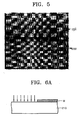
- a photograph of the etched substrate 210 is shown in FIG. 7.
- the etching depth is adjusted such that the height difference between the first surface 211 and the second surface 212 equals to that between the p-type and n-type electrodes 170 and 180 of the semiconductor laser diode chip 100. Dry etching is preferable.
- a masking process is carried out on the first and second surfaces 211 and 212 to define regions for the first and second metal layers 221 and 222.
- the first and second metal layers 221 and 222 are formed on the first and second surfaces 211 and 212, respectively, as shown in FIG. 6C.
- the first and second metal layers 221 and 222 have the same thickness.
- first and second metal layers 221 and 222 are formed on the first and second metal layers 221 and 222 to define regions for the first and second solder layers 231 and 232.
- an alloy of two or more selected from the group consisting of Cr, Ti, Pt, Au, Mo, and Sn, such as Au/Sn, Pt/Au/Sn, and Cr/Au/Sn, are deposited at a predetermined thickness.
- the first and second solder layers 231 and 232 are formed on the first and second metal layers 221 and 222, respectively, as shown in FIG. 6D.
- the first and second solder layers 231 and 232 are concurrently formed to the same thickness.
- the first and second solder layers 231 and 232 have almost the same chemical composition ratio.
- a submount having the same height difference between the first and second solder layers 231 and 232 as that between the p-type and n-type electrodes 170 and 180 can be formed.
- a semiconductor laser diode assembly and its manufacturing method of the present invention provide the following effects.
Landscapes
- Physics & Mathematics (AREA)
- Condensed Matter Physics & Semiconductors (AREA)
- General Physics & Mathematics (AREA)
- Electromagnetism (AREA)
- Optics & Photonics (AREA)
- Geometry (AREA)
- Semiconductor Lasers (AREA)
Applications Claiming Priority (2)
| Application Number | Priority Date | Filing Date | Title |
|---|---|---|---|
| KR1020030014613A KR100958054B1 (ko) | 2003-03-08 | 2003-03-08 | 반도체 레이저 다이오드의 서브 마운트, 그 제조방법 및이를 채용한 반도체 레이저 다이오드 조립체 |
| KR2003014613 | 2003-03-08 |
Publications (2)
| Publication Number | Publication Date |
|---|---|
| EP1458036A1 true EP1458036A1 (de) | 2004-09-15 |
| EP1458036B1 EP1458036B1 (de) | 2005-11-23 |
Family
ID=36776511
Family Applications (1)
| Application Number | Title | Priority Date | Filing Date |
|---|---|---|---|
| EP03257874A Expired - Lifetime EP1458036B1 (de) | 2003-03-08 | 2003-12-15 | Träger für eine Halbleiterlaserdiode, Verfahren um den Subträger herzustellen, und Halbleiterlaserdiode mit dem Träger |
Country Status (6)
| Country | Link |
|---|---|
| US (2) | US7092420B2 (de) |
| EP (1) | EP1458036B1 (de) |
| JP (1) | JP2004274057A (de) |
| KR (1) | KR100958054B1 (de) |
| CN (1) | CN100468893C (de) |
| DE (1) | DE60302427T2 (de) |
Cited By (2)
| Publication number | Priority date | Publication date | Assignee | Title |
|---|---|---|---|---|
| EP2280430A3 (de) * | 2005-03-11 | 2012-08-29 | Seoul Semiconductor Co., Ltd. | LED-Kapselung mit einer Gruppe in Reihe geschalteter Leuchtzellen |
| EP2063468A4 (de) * | 2006-10-13 | 2014-09-03 | Future Light Ltd Liability Company | Lichtemittierendes halbleiterbauelement, beleuchtungssystem und verfahren zur herstellung eines lichtemittierenden halbleiterbauelements |
Families Citing this family (32)
| Publication number | Priority date | Publication date | Assignee | Title |
|---|---|---|---|---|
| KR100964399B1 (ko) * | 2003-03-08 | 2010-06-17 | 삼성전자주식회사 | 반도체 레이저 다이오드 및 이를 채용한 반도체 레이저다이오드 조립체 |
| CN100576662C (zh) * | 2004-11-01 | 2009-12-30 | 中国科学院半导体研究所 | 利用倒装焊技术制作氮化镓基激光器管芯的方法 |
| JP2008523637A (ja) * | 2004-12-14 | 2008-07-03 | ソウル オプト−デバイス カンパニー リミテッド | 複数の発光セルを有する発光素子及びそれを搭載したパッケージ |
| KR101106148B1 (ko) * | 2004-12-14 | 2012-01-20 | 서울옵토디바이스주식회사 | 발광 소자 |
| KR101086995B1 (ko) * | 2004-12-29 | 2011-11-29 | 엘지전자 주식회사 | 발광 소자 조립용 서브 마운트 기판 및 그의 제조 방법 |
| KR101100425B1 (ko) * | 2005-05-07 | 2011-12-30 | 삼성전자주식회사 | 반도체 레이저 다이오드 및 그 제조방법 |
| KR100598357B1 (ko) * | 2005-05-24 | 2006-07-06 | 엘지전자 주식회사 | 발광소자용 서브마운트 기판 |
| US7816155B2 (en) * | 2007-07-06 | 2010-10-19 | Jds Uniphase Corporation | Mounted semiconductor device and a method for making the same |
| EP3525301B1 (de) * | 2007-12-28 | 2021-11-03 | Avago Technologies International Sales Pte. Limited | Vorrichtung mit delta-dotierter aktiver region |
| CN102202484B (zh) * | 2010-03-23 | 2014-04-16 | 施耐德东芝换流器欧洲公司 | 散热系统诊断方法 |
| US8456961B1 (en) | 2011-03-22 | 2013-06-04 | Western Digital (Fremont), Llc | Systems and methods for mounting and aligning a laser in an electrically assisted magnetic recording assembly |
| US8518748B1 (en) | 2011-06-29 | 2013-08-27 | Western Digital (Fremont), Llc | Method and system for providing a laser submount for an energy assisted magnetic recording head |
| US8288204B1 (en) | 2011-08-30 | 2012-10-16 | Western Digital (Fremont), Llc | Methods for fabricating components with precise dimension control |
| US8665677B1 (en) | 2011-12-19 | 2014-03-04 | Western Digital (Fremont), Llc | Disk drive magnetic read head with affixed and recessed laser device |
| US9475151B1 (en) | 2012-10-30 | 2016-10-25 | Western Digital (Fremont), Llc | Method and apparatus for attaching a laser diode and a slider in an energy assisted magnetic recording head |
| US9431037B2 (en) | 2013-03-12 | 2016-08-30 | Western Digitatl (Fremont), LLC | Systems and methods for monitoring the power of a light source utilized in energy-assisted magnetic recording |
| US8897102B1 (en) | 2013-04-02 | 2014-11-25 | Western Digital (Fremont), Llc | Method and system for measuring light delivery offsets in a heat assisted magnetic recording head |
| US9001628B1 (en) | 2013-12-16 | 2015-04-07 | Western Digital (Fremont), Llc | Assistant waveguides for evaluating main waveguide coupling efficiency and diode laser alignment tolerances for hard disk |
| CN104979224B (zh) * | 2014-04-04 | 2017-10-20 | 中国科学院苏州纳米技术与纳米仿生研究所 | 一种器件封装互联方法 |
| US9042048B1 (en) | 2014-09-30 | 2015-05-26 | Western Digital (Fremont), Llc | Laser-ignited reactive HAMR bonding |
| US9902023B1 (en) | 2014-10-28 | 2018-02-27 | Western Digital (Fremont), Llc | Systems and devices for achieving high throughput attachment and sub-micron alignment of components |
| WO2016190919A2 (en) * | 2015-01-30 | 2016-12-01 | University Of Southern California | Micro-vcsels in thermally engineered flexible composite assemblies |
| KR102373677B1 (ko) | 2015-08-24 | 2022-03-14 | 쑤저우 레킨 세미컨덕터 컴퍼니 리미티드 | 발광소자 |
| US20170105287A1 (en) * | 2015-10-12 | 2017-04-13 | Tyco Electronics Corporation | Process of Producing Electronic Component and an Electronic Component |
| TWI620352B (zh) * | 2017-01-20 | 2018-04-01 | 大光能源科技有限公司 | 覆晶發光二極體及其製造方法 |
| CN110289548B (zh) * | 2019-06-17 | 2021-04-27 | 威科赛乐微电子股份有限公司 | flip chip型VCSEL芯片及其制造方法 |
| DE102020132133A1 (de) | 2020-12-03 | 2022-06-09 | OSRAM Opto Semiconductors Gesellschaft mit beschränkter Haftung | Strahlungsemittierendes laserbauteil und verfahren zur herstellung eines strahlungsemittierenden laserbauteils |
| US11876343B2 (en) | 2021-05-18 | 2024-01-16 | Trumpf Photonics, Inc. | Laser diode packaging platforms |
| US11557874B2 (en) * | 2021-05-18 | 2023-01-17 | Trumpf Photonics, Inc. | Double-sided cooling of laser diodes |
| KR20230064001A (ko) * | 2021-11-01 | 2023-05-10 | 삼성디스플레이 주식회사 | 표시 장치 및 이의 제조 방법 |
| CN114908320A (zh) * | 2022-04-14 | 2022-08-16 | 广东工业大学 | 一种免刻蚀的半导体激光器热沉结构及其制备方法和应用 |
| CN116613626B (zh) * | 2023-07-21 | 2023-09-26 | 南昌凯迅光电股份有限公司 | 一种AuSn电极背面出光VCSEL芯片及其制备方法 |
Citations (5)
| Publication number | Priority date | Publication date | Assignee | Title |
|---|---|---|---|---|
| US6242764B1 (en) * | 1997-07-17 | 2001-06-05 | Kabushiki Kaisha Toshiba | III-N semiconductor light-emitting element having strain-moderating crystalline buffer layers |
| US20010006235A1 (en) * | 1999-12-09 | 2001-07-05 | Masafumi Ozawa | Semiconductor light-emitting device and method of manufacturing the same and mounting plate |
| US6266355B1 (en) * | 1997-09-12 | 2001-07-24 | Sdl, Inc. | Group III-V nitride laser devices with cladding layers to suppress defects such as cracking |
| KR20020048546A (ko) * | 2000-12-18 | 2002-06-24 | 이형도 | GaN계열 Ⅲ-Ⅴ족 질화물 반도체 발광 소자 및 그 제조방법 |
| US6657237B2 (en) * | 2000-12-18 | 2003-12-02 | Samsung Electro-Mechanics Co., Ltd. | GaN based group III-V nitride semiconductor light-emitting diode and method for fabricating the same |
Family Cites Families (9)
| Publication number | Priority date | Publication date | Assignee | Title |
|---|---|---|---|---|
| GB8728342D0 (en) * | 1987-12-03 | 1988-01-06 | Bt & D Technologies Ltd | Light sources |
| TW381411B (en) * | 1997-01-20 | 2000-02-01 | Oki Electric Ind Co Ltd | Assembly unit for optical semiconductor components and the supporting substrate and the method for embedding optical semiconductor components on the supporting substrate |
| US6281524B1 (en) * | 1997-02-21 | 2001-08-28 | Kabushiki Kaisha Toshiba | Semiconductor light-emitting device |
| JP2001168442A (ja) | 1999-12-07 | 2001-06-22 | Sony Corp | 半導体レーザ素子の製造方法、配設基板および支持基板 |
| JP2001339121A (ja) * | 2000-05-29 | 2001-12-07 | Sharp Corp | 窒化物半導体発光素子とそれを含む光学装置 |
| US6630689B2 (en) * | 2001-05-09 | 2003-10-07 | Lumileds Lighting, U.S. Llc | Semiconductor LED flip-chip with high reflectivity dielectric coating on the mesa |
| KR100789112B1 (ko) * | 2002-02-06 | 2007-12-26 | 주식회사 엘지이아이 | 화합물 반도체 발광 소자의 제조 방법 |
| JP3882712B2 (ja) * | 2002-08-09 | 2007-02-21 | 住友電気工業株式会社 | サブマウントおよび半導体装置 |
| KR101086995B1 (ko) * | 2004-12-29 | 2011-11-29 | 엘지전자 주식회사 | 발광 소자 조립용 서브 마운트 기판 및 그의 제조 방법 |
-
2003
- 2003-03-08 KR KR1020030014613A patent/KR100958054B1/ko not_active Expired - Fee Related
- 2003-12-09 CN CNB200310120206XA patent/CN100468893C/zh not_active Expired - Lifetime
- 2003-12-11 US US10/732,241 patent/US7092420B2/en not_active Expired - Lifetime
- 2003-12-15 DE DE60302427T patent/DE60302427T2/de not_active Expired - Lifetime
- 2003-12-15 EP EP03257874A patent/EP1458036B1/de not_active Expired - Lifetime
-
2004
- 2004-03-05 JP JP2004062190A patent/JP2004274057A/ja not_active Withdrawn
-
2006
- 2006-06-30 US US11/477,911 patent/US20070015313A1/en not_active Abandoned
Patent Citations (5)
| Publication number | Priority date | Publication date | Assignee | Title |
|---|---|---|---|---|
| US6242764B1 (en) * | 1997-07-17 | 2001-06-05 | Kabushiki Kaisha Toshiba | III-N semiconductor light-emitting element having strain-moderating crystalline buffer layers |
| US6266355B1 (en) * | 1997-09-12 | 2001-07-24 | Sdl, Inc. | Group III-V nitride laser devices with cladding layers to suppress defects such as cracking |
| US20010006235A1 (en) * | 1999-12-09 | 2001-07-05 | Masafumi Ozawa | Semiconductor light-emitting device and method of manufacturing the same and mounting plate |
| KR20020048546A (ko) * | 2000-12-18 | 2002-06-24 | 이형도 | GaN계열 Ⅲ-Ⅴ족 질화물 반도체 발광 소자 및 그 제조방법 |
| US6657237B2 (en) * | 2000-12-18 | 2003-12-02 | Samsung Electro-Mechanics Co., Ltd. | GaN based group III-V nitride semiconductor light-emitting diode and method for fabricating the same |
Cited By (2)
| Publication number | Priority date | Publication date | Assignee | Title |
|---|---|---|---|---|
| EP2280430A3 (de) * | 2005-03-11 | 2012-08-29 | Seoul Semiconductor Co., Ltd. | LED-Kapselung mit einer Gruppe in Reihe geschalteter Leuchtzellen |
| EP2063468A4 (de) * | 2006-10-13 | 2014-09-03 | Future Light Ltd Liability Company | Lichtemittierendes halbleiterbauelement, beleuchtungssystem und verfahren zur herstellung eines lichtemittierenden halbleiterbauelements |
Also Published As
| Publication number | Publication date |
|---|---|
| EP1458036B1 (de) | 2005-11-23 |
| CN100468893C (zh) | 2009-03-11 |
| KR100958054B1 (ko) | 2010-05-13 |
| US7092420B2 (en) | 2006-08-15 |
| US20050002428A1 (en) | 2005-01-06 |
| JP2004274057A (ja) | 2004-09-30 |
| US20070015313A1 (en) | 2007-01-18 |
| KR20040079635A (ko) | 2004-09-16 |
| DE60302427D1 (de) | 2005-12-29 |
| CN1527448A (zh) | 2004-09-08 |
| DE60302427T2 (de) | 2006-08-24 |
Similar Documents
| Publication | Publication Date | Title |
|---|---|---|
| EP1458036B1 (de) | Träger für eine Halbleiterlaserdiode, Verfahren um den Subträger herzustellen, und Halbleiterlaserdiode mit dem Träger | |
| CN100452447C (zh) | GaN基Ⅲ-Ⅴ族氮化物发光二极管及其制造方法 | |
| US20070110113A1 (en) | Semiconductor laser diode and semiconductor laser diode assembly containing the same | |
| JP2013102240A (ja) | 二重ヘテロ構造の発光領域を有するiii族窒化物発光デバイス | |
| KR101960128B1 (ko) | 레이저 다이오드 디바이스 | |
| US7406111B2 (en) | Semiconductor laser diode and method for manufacturing the same | |
| JPH10223930A (ja) | 半導体発光素子 | |
| US7606275B2 (en) | Semiconductor laser device having incomplete bonding region and electronic equipment | |
| KR100397608B1 (ko) | GaN계열 Ⅲ-Ⅴ족 질화물 반도체 레이저 다이오드 | |
| CN100461469C (zh) | GaN基Ⅲ-Ⅴ族氮化物发光二极管及其制造方法 | |
| KR100922847B1 (ko) | 레이저 다이오드 및 그 제조방법 | |
| US20070158665A1 (en) | Light emitting diode | |
| KR100644215B1 (ko) | 발광소자와 그 제조방법 | |
| WO2005057745A1 (en) | Gan-based vertical electrode laser diode utilizing the technique of sapphire etching and manufacturing method of the same. | |
| KR101013621B1 (ko) | 반도체 레이저 다이오드 및 그 제조 방법 | |
| WO2025056620A1 (en) | Optoelectronic device and method of processing the same |
Legal Events
| Date | Code | Title | Description |
|---|---|---|---|
| PUAI | Public reference made under article 153(3) epc to a published international application that has entered the european phase |
Free format text: ORIGINAL CODE: 0009012 |
|
| AK | Designated contracting states |
Kind code of ref document: A1 Designated state(s): AT BE BG CH CY CZ DE DK EE ES FI FR GB GR HU IE IT LI LU MC NL PT RO SE SI SK TR |
|
| AX | Request for extension of the european patent |
Extension state: AL LT LV MK |
|
| 17P | Request for examination filed |
Effective date: 20050112 |
|
| 17Q | First examination report despatched |
Effective date: 20050308 |
|
| GRAP | Despatch of communication of intention to grant a patent |
Free format text: ORIGINAL CODE: EPIDOSNIGR1 |
|
| AKX | Designation fees paid |
Designated state(s): DE FR GB |
|
| GRAS | Grant fee paid |
Free format text: ORIGINAL CODE: EPIDOSNIGR3 |
|
| GRAA | (expected) grant |
Free format text: ORIGINAL CODE: 0009210 |
|
| AK | Designated contracting states |
Kind code of ref document: B1 Designated state(s): DE FR GB |
|
| REG | Reference to a national code |
Ref country code: GB Ref legal event code: FG4D |
|
| REF | Corresponds to: |
Ref document number: 60302427 Country of ref document: DE Date of ref document: 20051229 Kind code of ref document: P |
|
| ET | Fr: translation filed | ||
| PLBE | No opposition filed within time limit |
Free format text: ORIGINAL CODE: 0009261 |
|
| STAA | Information on the status of an ep patent application or granted ep patent |
Free format text: STATUS: NO OPPOSITION FILED WITHIN TIME LIMIT |
|
| 26N | No opposition filed |
Effective date: 20060824 |
|
| REG | Reference to a national code |
Ref country code: FR Ref legal event code: PLFP Year of fee payment: 13 |
|
| REG | Reference to a national code |
Ref country code: FR Ref legal event code: PLFP Year of fee payment: 14 |
|
| REG | Reference to a national code |
Ref country code: FR Ref legal event code: PLFP Year of fee payment: 15 |
|
| PGFP | Annual fee paid to national office [announced via postgrant information from national office to epo] |
Ref country code: FR Payment date: 20221021 Year of fee payment: 20 |
|
| PGFP | Annual fee paid to national office [announced via postgrant information from national office to epo] |
Ref country code: GB Payment date: 20221027 Year of fee payment: 20 Ref country code: DE Payment date: 20220622 Year of fee payment: 20 |
|
| P01 | Opt-out of the competence of the unified patent court (upc) registered |
Effective date: 20230520 |
|
| REG | Reference to a national code |
Ref country code: DE Ref legal event code: R071 Ref document number: 60302427 Country of ref document: DE |
|
| REG | Reference to a national code |
Ref country code: GB Ref legal event code: PE20 Expiry date: 20231214 |
|
| PG25 | Lapsed in a contracting state [announced via postgrant information from national office to epo] |
Ref country code: GB Free format text: LAPSE BECAUSE OF EXPIRATION OF PROTECTION Effective date: 20231214 |
|
| PG25 | Lapsed in a contracting state [announced via postgrant information from national office to epo] |
Ref country code: GB Free format text: LAPSE BECAUSE OF EXPIRATION OF PROTECTION Effective date: 20231214 |