EP1460838A1 - Bildaufnahmevorrichtung, Verfahren zur Steuerung solcher Vorrichtung und elektrisches Signal erzeugt von einer solchen Vorrichtung - Google Patents
Bildaufnahmevorrichtung, Verfahren zur Steuerung solcher Vorrichtung und elektrisches Signal erzeugt von einer solchen Vorrichtung Download PDFInfo
- Publication number
- EP1460838A1 EP1460838A1 EP03290690A EP03290690A EP1460838A1 EP 1460838 A1 EP1460838 A1 EP 1460838A1 EP 03290690 A EP03290690 A EP 03290690A EP 03290690 A EP03290690 A EP 03290690A EP 1460838 A1 EP1460838 A1 EP 1460838A1
- Authority
- EP
- European Patent Office
- Prior art keywords
- value
- generating
- voltage
- detection node
- sensitive element
- Prior art date
- Legal status (The legal status is an assumption and is not a legal conclusion. Google has not performed a legal analysis and makes no representation as to the accuracy of the status listed.)
- Withdrawn
Links
Images



Classifications
-
- H—ELECTRICITY
- H04—ELECTRIC COMMUNICATION TECHNIQUE
- H04N—PICTORIAL COMMUNICATION, e.g. TELEVISION
- H04N25/00—Circuitry of solid-state image sensors [SSIS]; Control thereof
- H04N25/50—Control of the SSIS exposure
- H04N25/57—Control of the dynamic range
- H04N25/571—Control of the dynamic range involving a non-linear response
- H04N25/575—Control of the dynamic range involving a non-linear response with a response composed of multiple slopes
-
- H—ELECTRICITY
- H04—ELECTRIC COMMUNICATION TECHNIQUE
- H04N—PICTORIAL COMMUNICATION, e.g. TELEVISION
- H04N25/00—Circuitry of solid-state image sensors [SSIS]; Control thereof
- H04N25/50—Control of the SSIS exposure
- H04N25/57—Control of the dynamic range
- H04N25/58—Control of the dynamic range involving two or more exposures
- H04N25/587—Control of the dynamic range involving two or more exposures acquired sequentially, e.g. using the combination of odd and even image fields
- H04N25/589—Control of the dynamic range involving two or more exposures acquired sequentially, e.g. using the combination of odd and even image fields with different integration times, e.g. short and long exposures
-
- H—ELECTRICITY
- H04—ELECTRIC COMMUNICATION TECHNIQUE
- H04N—PICTORIAL COMMUNICATION, e.g. TELEVISION
- H04N25/00—Circuitry of solid-state image sensors [SSIS]; Control thereof
- H04N25/70—SSIS architectures; Circuits associated therewith
- H04N25/76—Addressed sensors, e.g. MOS or CMOS sensors
- H04N25/77—Pixel circuitry, e.g. memories, A/D converters, pixel amplifiers, shared circuits or shared components
-
- H—ELECTRICITY
- H04—ELECTRIC COMMUNICATION TECHNIQUE
- H04N—PICTORIAL COMMUNICATION, e.g. TELEVISION
- H04N25/00—Circuitry of solid-state image sensors [SSIS]; Control thereof
- H04N25/70—SSIS architectures; Circuits associated therewith
- H04N25/76—Addressed sensors, e.g. MOS or CMOS sensors
- H04N25/77—Pixel circuitry, e.g. memories, A/D converters, pixel amplifiers, shared circuits or shared components
- H04N25/771—Pixel circuitry, e.g. memories, A/D converters, pixel amplifiers, shared circuits or shared components comprising storage means other than floating diffusion
-
- H—ELECTRICITY
- H04—ELECTRIC COMMUNICATION TECHNIQUE
- H04N—PICTORIAL COMMUNICATION, e.g. TELEVISION
- H04N25/00—Circuitry of solid-state image sensors [SSIS]; Control thereof
- H04N25/70—SSIS architectures; Circuits associated therewith
- H04N25/76—Addressed sensors, e.g. MOS or CMOS sensors
- H04N25/77—Pixel circuitry, e.g. memories, A/D converters, pixel amplifiers, shared circuits or shared components
- H04N25/772—Pixel circuitry, e.g. memories, A/D converters, pixel amplifiers, shared circuits or shared components comprising A/D, V/T, V/F, I/T or I/F converters
-
- H—ELECTRICITY
- H04—ELECTRIC COMMUNICATION TECHNIQUE
- H04N—PICTORIAL COMMUNICATION, e.g. TELEVISION
- H04N25/00—Circuitry of solid-state image sensors [SSIS]; Control thereof
- H04N25/70—SSIS architectures; Circuits associated therewith
- H04N25/76—Addressed sensors, e.g. MOS or CMOS sensors
- H04N25/78—Readout circuits for addressed sensors, e.g. output amplifiers or A/D converters
Definitions
- the invention relates to an image sensing device, to a process for driving such a device and to a signal generated in such a device.
- light-sensitive elements arranged as a matrix convert impinging light (photons) received during an integration time into a corresponding charge.
- the charge output by each element is then used as an indicator of the light received by this element, and therefore as a measure of the light received from a given direction.
- the sensitivity of the sensing device naturally depends on the integration time.
- Patent references EP 0 387 817, US 5,309,243, US 5,671,013 and JP 2001 - 346 096 describe solutions where each of the two pictures is stored in a memory external to the image sensor. The two pictures are then combined by appropriate processing into a picture with increased dynamic range.
- patent application EP 1 003 329 proposes to combine the two measurements into an output value immediately after the measurements are made.
- this solution requires digital processing in the image sensor itself to combine the two measurements, which makes the image sensor more complex and thus more expensive.
- Patent application EP 1 233 613 describes an alternative solution in which each pixel element is reset only when a predetermined charge has accumulated. When the charge has not reached the predetermined value, the reset is skipped. For each pixel, the number of reset skips is thus used as a further indicator of the incoming light in addition to the conventional charge peak value.
- this solution needs a complex architecture to select the pixels which have to be reset.
- the invention seeks a cost-effective and simple solution for a image sensing device with increased dynamic range.
- the invention proposes a process for driving an image sensing device having an image cell with a photo-sensitive element, a detection node and an output pin, comprising the steps of :
- the two values are available at the level of the image cell without the need for a complex construction.
- the step of generating the first value is separated from the step of transferring charges accumulated during the first period by approximately the second period. It is then taken advantage of the detection node to store the first voltage during the second period, so that the two values can be output in a limited period of time.
- the step of generating the first value occurs more than 20 ⁇ s later (and preferably more than 1 ms later) than the step of transferring charges accumulated during the first period and the step of generating the second value occurs less than 20 ⁇ s later (and preferably less than 100 ⁇ s) than the step of generating the first value.
- the step of generating the first value occurs at least one line time minus a blanking interval time later than the step of transferring charges accumulated during the first period, whereas the step of generating the second value occurs less than the blanking interval time later than the step of generating the first value.
- the step of generating the first value and generating the second value occur during a single horizontal blanking interval. This fully takes advantage of the detection node to store the first voltage while outputting the first and second value in the short horizontal blanking interval.
- the following steps are also realised in the image sensing device :
- the invention results in a process for driving an image sensing device having a first image cell with a first photo-sensitive element, a first detection node and a first output pin, and a second image cell with a second photo-sensitive element, a second detection node and a second output pin, the first output pin and the second output pin being connected to a common output wire, comprising the steps of :
- the values for a given image cell are grouped together thanks notably to the use of the detection nodes to store voltages.
- this process further comprises the steps of :
- the invention consequently proposes an electrical signal generated in an image sensing device having a first image cell and a second image cell, taking over increasing time :
- the image sensing device has an image cell with a photo-sensitive element, a detection node and an output pin, and comprises transfer means for transferring charges from the photo-sensitive element to the detection node, read-out means for generating on the output pin a value based on the detection node voltage and driving means for controlling the transfer means and the read-out means so that at least two values are generated during an integration period.
- the image sensing device comprises comparator means for comparing at least one of said two values to a reference value.
- steps and parts of signal are ordered as indicated but that they may be separated by other steps, such as steps to deal with the reset noise, as described below.
- An imager comprises a matrix of pixels or image cells.
- FIG. 1a shows in detail an image cell IC n .
- the image cell IC n comprises a photodiode which is the light-sensitive element of the image cell : the photodiode ⁇ D creates an amount of charges depending on the quantity of light it receives.
- the photodiode ⁇ D is connected to a first plate of a capacitor C through a CMOS transistor T1 (transfer gate).
- the second plate of capacitor C is grounded.
- the first plate of capacitor C is also connected to ground via a CMOS transistor T3 (reset transistor) which can therefore reset (i.e. put to a reference value the voltage across) capacitor C.
- the first plate of capacitor C is connected to an output pin of the image cell IC n via CMOS transistors T2 (buffer transistor) and T4 (read-out or row address transistor), which allows to send out the value measured by the image cell IC n .
- CMOS transistors T2 (buffer transistor) and T4 (read-out or row address transistor) which allows to send out the value measured by the image cell IC n .
- row has the same meaning as line.
- the first plate of capacitor C thus realises a detection node.
- the transfer gate T1, the reset transistor T3 and the read-out transistor T4 are controlled by driving signals (respectively DS1, DS3 and DS4) as represented respectively on Figures 2a to 2c and further described later.
- Buffer transistor T2 is biased by a voltage V+ (which can be either a constant voltage or active only when it is needed).
- Figure 1b represents three image cells IC 1 , IC 2 and IC 3 with their respective output connected to a read-out column ROC.
- Each image cell IC n of a column of the pixel matrix is similarly connected to a corresponding read-out column ROC.
- Each read-out column ROC transmits the measured values from the image cells of a column to a read-out circuit RC m dedicated to process the values of the column.
- Each column thus has a dedicated read-out circuit RC m .
- a read-out circuit RCm comprises a comparator COMP having a first input at a reference voltage V comp and a second input connected to the read-out column ROC.
- the result of the comparison is used as an extended dynamic range (EDR) signal as will be further described below.
- EDR extended dynamic range
- the read-out column ROC carrying the various measured values, it is also connected to an output pin labelled POV (for Pixel Output Value) through a multiplier (by 0, +1 or -1 depending on the considered moment as further explained below) and an (integrating) amplifier.
- POV Pixel Output Value
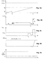
- Figures 3a to 3e illustrate how the image sensing device operates in a first possible case where the pixel typically receives a low to medium quantity of light.
- Figure 3a represents the charges accumulated by the light sensitive element at a pixel over an integration period I.
- the voltage at the detection node (illustrated on Figure 3b) is reset by closing reset transistor T3 shortly (by driving signal DS3, see Figure 2b) and the detection node thus carries a reset noise voltage R 1 .
- the light sensitive element has accumulated an amount Q 1 of charges and the transfer gate T1 is shortly closed (by driving signal DS1, see Figure 2a) in order to transfer the charges Q1 from the light sensitive element (photodiode ⁇ D) to the detection node (capacitor C), thereby rising the voltage at the detection node by a value V 1 .
- the detection node has then the value R 1 +V 1 .
- the light sensitive element After t1, the light sensitive element accumulates charges again, over a second period I 2 , preferably longer than I 1 .
- read-out transistor T4 is closed (see Figure 2c) to output the voltage at the detection node (R 1 +V 1 ) to the read-out column ROC, where it is compared by the comparator to a reference value V comp .
- the read-out values V ROC are represented on Figure 3c.
- the voltage from the detection node (R 1 +V 1 ) is lower than the reference voltage V comp , which means that assumption can be made that the pixel does not clip over the second (longer) period I 2 .
- the second example made with reference to Figures 4a to 4e describes operation when R1+V1 > V comp .
- the charges accumulated during the second period I 2 can thus be used as a basis for the value to be output for this pixel.
- the voltage at the detection node is reset by shortly closing the reset transistor T3 (moment t 3 , see Figure 2b) and thus carries a reset noise voltage R 2 , which is read-out immediately at the read-out column ROC and integrated at the column-amplifier with a negative sign (see Figure 3d).
- the transfer gate T1 is closed (see Figure 2a) in order to transfer the charges Q 2 accumulated by the light sensitive element during the second period to the detection node.
- the voltage at the detection node therefore increases by a value V 2 corresponding to charges Q 2 .
- the voltage at the detection node is R 2 +V 2 .
- the steps taken from t 2 to t 4 occur during the horizontal blanking interval HB (immediately before the line comprising the image cell is output in the video signal). As these steps may create noise, this avoids that disturbances appear on active parts of the video signal.
- the duration (t 4 -t 2 ) is preferably within the range of several micro-seconds, for instance between 5 and 10 ⁇ s.
- the output value is thus the correct measured value, without the reset noise.
- the value V 2 can also be multiplied by N/(N-1) to be precisely equal to the value it would have had if it had been integrated over the whole integration period I.
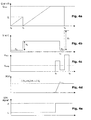
- Figures 4a to 4e illustrate how the image sensing device operates in a second possible case where the pixel typically receives a high quantity of light.
- Figure 4a represents the charges accumulated by the light sensitive element at the pixel over the integration period I. As previously, charges accumulate from the starting point t 0 of the integration period, during the first period I 1 ending at t 1 . As explained above, at t 0 , the voltage at the detection node (illustrated on Figure 4b) is reset by closing reset gate T3 and the detection node thus carries a reset noise voltage R 1 .
- the light sensitive element has accumulated an amount Q 1 of charges and the transfer gate T1 is closed in order to transfer the charges Q1 from the light sensitive element (photodiode ⁇ D) to the detection node (capacitor C), thereby rising the voltage at the detection node by the value V 1 .
- the detection node has then the value R 1 +V 1 .
- the light sensitive element After t1, the light sensitive element accumulates charges again, over the second period I 2 , preferably longer than I 1 .
- the maximum amount of charges Q max acceptable by the light-sensitive element is reached before the end of the integration period (i.e. also before the end of the second period I 2 ) : the pixel clips. This has the consequence that the amount of charges and the derived voltage will not accurately represent the amount of light received by the pixel over the second period I 2 .
- read-out transistor T4 is closed to output the voltage at the detection node (R 1 +V 1 ) to the read-out column, where it is compared by the comparator to the reference value V comp .
- the read-out values are represented on Figure 4c.
- the voltage from the detection node (R 1 +V 1 ) is larger than the reference voltage V comp . This is indicative that the pixel clips over the second period I 2 for the following reasons :
- the value (R 1 +V 1 ) measured over the (shorter) first period I 1 is more representative of the quantity of light received by the light sensitive element and will be used to compute the pixel output value (POV) out of the column amplifier ( Figure 4d).
- the output of the comparator sends out a high Extended Dynamic Range signal (see Figure 4e) to indicate to further processing entitles that the output value V 1 was measured during the period I 1 .
- the pixel output value shall be multiplied by N-1 by further processing steps (or by N if the value is corrected by a factor N/(N-1) when the Extended Dynamic Range is low - see above).
- the voltage (R 1 +V 1 ) read-out at moment t 2 besides being used on the comparator input, is in this case integrated at the column-amplifier with a positive sign.
- the voltage at the detection node is reset by shortly closing the reset transistor T3 (moment t 3 ) and thus carries a reset noise voltage R2, which is read-out immediately at the read-out column and integrated at the column-amplifier with a negative sign (see Figure 4d).
- the output value is thus a very close measure for the correct measured value as R1 and R2 are only noise values.
- the clipped value (R 2 +V 2 ) is read-out to the read-out column ROC by closing read-out gates T2 and T4 but it is not integrated at the column amplifier because of the result of the comparison realised by the comparator : (R 1 +V 1 ) > V comp .
- the read-out circuit RC m does not select between the first and second measured values but transmits them both to a further processing stage together with the extended dynamic range (EDR) signal.
- EDR extended dynamic range
- the output values thus correspond to the voltages carried by the read-out column ROC, as shown on Figure 5.
- image cells IC 1 and IC 3 clips over the second period I 2 ; correspondingly, the EDR signal is set to a high level H, indicating to further processing stages that the first measured value, respectively (R 1 +V 1 ) (IC1) and (R 1 +V 1 ) (IC3) , should preferably be used.
- image cell IC 2 does not clip and the EDR signal is low (level L) for this image cell indicating that (R 2 +V 2 ) (IC2) should preferably be used.
- CMOS imager uses a CMOS imager
- CCD imager uses a CCD imager
Landscapes
- Engineering & Computer Science (AREA)
- Multimedia (AREA)
- Signal Processing (AREA)
- Physics & Mathematics (AREA)
- Nonlinear Science (AREA)
- Solid State Image Pick-Up Elements (AREA)
- Transforming Light Signals Into Electric Signals (AREA)
Priority Applications (4)
| Application Number | Priority Date | Filing Date | Title |
|---|---|---|---|
| EP03290690A EP1460838A1 (de) | 2003-03-18 | 2003-03-18 | Bildaufnahmevorrichtung, Verfahren zur Steuerung solcher Vorrichtung und elektrisches Signal erzeugt von einer solchen Vorrichtung |
| EP04718205A EP1609306A1 (de) | 2003-03-18 | 2004-03-06 | Bilderfassungseinrichtung, prozess zur ansteuerung einer solchen einrichtung und in einer solchen einrichtung erzeugtes elektrisches signal |
| PCT/EP2004/002325 WO2004084543A1 (en) | 2003-03-18 | 2004-03-06 | Image sensing device, process for driving such a device and electrical signal generated in such a device |
| US10/549,133 US7528876B2 (en) | 2003-03-18 | 2004-03-06 | Image sensing device, process for driving such a device and electrical signal generated in such a device |
Applications Claiming Priority (1)
| Application Number | Priority Date | Filing Date | Title |
|---|---|---|---|
| EP03290690A EP1460838A1 (de) | 2003-03-18 | 2003-03-18 | Bildaufnahmevorrichtung, Verfahren zur Steuerung solcher Vorrichtung und elektrisches Signal erzeugt von einer solchen Vorrichtung |
Publications (1)
| Publication Number | Publication Date |
|---|---|
| EP1460838A1 true EP1460838A1 (de) | 2004-09-22 |
Family
ID=32799125
Family Applications (2)
| Application Number | Title | Priority Date | Filing Date |
|---|---|---|---|
| EP03290690A Withdrawn EP1460838A1 (de) | 2003-03-18 | 2003-03-18 | Bildaufnahmevorrichtung, Verfahren zur Steuerung solcher Vorrichtung und elektrisches Signal erzeugt von einer solchen Vorrichtung |
| EP04718205A Withdrawn EP1609306A1 (de) | 2003-03-18 | 2004-03-06 | Bilderfassungseinrichtung, prozess zur ansteuerung einer solchen einrichtung und in einer solchen einrichtung erzeugtes elektrisches signal |
Family Applications After (1)
| Application Number | Title | Priority Date | Filing Date |
|---|---|---|---|
| EP04718205A Withdrawn EP1609306A1 (de) | 2003-03-18 | 2004-03-06 | Bilderfassungseinrichtung, prozess zur ansteuerung einer solchen einrichtung und in einer solchen einrichtung erzeugtes elektrisches signal |
Country Status (3)
| Country | Link |
|---|---|
| US (1) | US7528876B2 (de) |
| EP (2) | EP1460838A1 (de) |
| WO (1) | WO2004084543A1 (de) |
Cited By (1)
| Publication number | Priority date | Publication date | Assignee | Title |
|---|---|---|---|---|
| EP1805801A4 (de) * | 2004-10-29 | 2009-12-09 | Mtek Vision Co Ltd | Bildsensor mit expandierendem dynamikumfang |
Families Citing this family (1)
| Publication number | Priority date | Publication date | Assignee | Title |
|---|---|---|---|---|
| US20090102939A1 (en) * | 2007-10-18 | 2009-04-23 | Narendra Ahuja | Apparatus and method for simultaneously acquiring multiple images with a given camera |
Citations (4)
| Publication number | Priority date | Publication date | Assignee | Title |
|---|---|---|---|---|
| JPH09200617A (ja) * | 1996-01-12 | 1997-07-31 | Nikon Corp | 撮像装置 |
| US6008486A (en) * | 1997-12-31 | 1999-12-28 | Gentex Corporation | Wide dynamic range optical sensor |
| US6011251A (en) * | 1997-06-04 | 2000-01-04 | Imec | Method for obtaining a high dynamic range read-out signal of a CMOS-based pixel structure and such CMOS-based pixel structure |
| JP2000092396A (ja) * | 1998-09-16 | 2000-03-31 | Olympus Optical Co Ltd | 増幅型固体撮像素子を用いた撮像装置 |
Family Cites Families (9)
| Publication number | Priority date | Publication date | Assignee | Title |
|---|---|---|---|---|
| EP0387817A3 (de) | 1989-03-16 | 1991-12-11 | Konica Corporation | Elektronische Standbild-Kamera |
| JP3528184B2 (ja) | 1991-10-31 | 2004-05-17 | ソニー株式会社 | 画像信号の輝度補正装置及び輝度補正方法 |
| US5309243A (en) | 1992-06-10 | 1994-05-03 | Eastman Kodak Company | Method and apparatus for extending the dynamic range of an electronic imaging system |
| DE69833998T2 (de) | 1998-11-18 | 2007-04-05 | C.S.E.M. Centre Suisse D'electronique Et De Microtechnique S.A. | Bilderzeugungsverfahren und -vorrichtung |
| JP4403635B2 (ja) | 2000-05-31 | 2010-01-27 | パナソニック株式会社 | ダイナミックレンジ拡大カメラ |
| US7050094B2 (en) * | 2000-10-26 | 2006-05-23 | Micron Technology, Inc. | Wide dynamic range operation for CMOS sensor with freeze-frame shutter |
| DE10064184C1 (de) | 2000-12-22 | 2002-04-04 | Fraunhofer Ges Forschung | Verfahren und Vorrichtung zur Bilderzeugung unter Verwendung mehrerer Belichtungszeiten |
| US7079178B2 (en) | 2001-02-20 | 2006-07-18 | Jaroslav Hynecek | High dynamic range active pixel CMOS image sensor and data processing system incorporating adaptive pixel reset |
| US6590610B2 (en) * | 2001-12-10 | 2003-07-08 | Motorola, Inc. | Digital double sampling in time integrating pixel sensors |
-
2003
- 2003-03-18 EP EP03290690A patent/EP1460838A1/de not_active Withdrawn
-
2004
- 2004-03-06 EP EP04718205A patent/EP1609306A1/de not_active Withdrawn
- 2004-03-06 WO PCT/EP2004/002325 patent/WO2004084543A1/en not_active Ceased
- 2004-03-06 US US10/549,133 patent/US7528876B2/en not_active Expired - Lifetime
Patent Citations (4)
| Publication number | Priority date | Publication date | Assignee | Title |
|---|---|---|---|---|
| JPH09200617A (ja) * | 1996-01-12 | 1997-07-31 | Nikon Corp | 撮像装置 |
| US6011251A (en) * | 1997-06-04 | 2000-01-04 | Imec | Method for obtaining a high dynamic range read-out signal of a CMOS-based pixel structure and such CMOS-based pixel structure |
| US6008486A (en) * | 1997-12-31 | 1999-12-28 | Gentex Corporation | Wide dynamic range optical sensor |
| JP2000092396A (ja) * | 1998-09-16 | 2000-03-31 | Olympus Optical Co Ltd | 増幅型固体撮像素子を用いた撮像装置 |
Non-Patent Citations (2)
| Title |
|---|
| PATENT ABSTRACTS OF JAPAN vol. 1997, no. 11 28 November 1997 (1997-11-28) * |
| PATENT ABSTRACTS OF JAPAN vol. 2000, no. 06 22 September 2000 (2000-09-22) * |
Cited By (1)
| Publication number | Priority date | Publication date | Assignee | Title |
|---|---|---|---|---|
| EP1805801A4 (de) * | 2004-10-29 | 2009-12-09 | Mtek Vision Co Ltd | Bildsensor mit expandierendem dynamikumfang |
Also Published As
| Publication number | Publication date |
|---|---|
| EP1609306A1 (de) | 2005-12-28 |
| US20060284995A1 (en) | 2006-12-21 |
| WO2004084543A1 (en) | 2004-09-30 |
| US7528876B2 (en) | 2009-05-05 |
Similar Documents
| Publication | Publication Date | Title |
|---|---|---|
| EP1078390B1 (de) | Aktivpixel-cmos-sensor mit mehreren speicherkondensator | |
| US7733401B2 (en) | Image capturing apparatus | |
| KR100552946B1 (ko) | 확장된 동적 범위의 이미지 센서 시스템 | |
| US5978025A (en) | Adaptive optical sensor | |
| US5258845A (en) | Solid-state image sensor driving device with signal synthesizing | |
| US5812703A (en) | Imaging apparatus | |
| EP0707416A2 (de) | Bildsensor mit aktiven Bildelementen und Abbildungssystem mit differentieller Betriebsweise | |
| EP1928166A2 (de) | Bildsensoren mit Vorrichtungen zur Reduzierung des Ausgangsrauschens | |
| US7256378B2 (en) | Output-compensating device for image sensor | |
| EP2538659B1 (de) | Bildaufnahmegerät | |
| JPH114385A (ja) | Cmosを基礎とするピクセル構造の高ダイナミックレンジの読み出し信号を得る方法及びそのcmosを基礎とするピクセル構造 | |
| US6995797B2 (en) | Charge detecting device for a solid state imaging device | |
| EP1943831B1 (de) | Bildsensor | |
| US5144444A (en) | Method and apparatus for improving the output response of an electronic imaging system | |
| US5659359A (en) | Image sensing system with electronic shutter and equal field exposure times in frame readout mode | |
| JP2003046864A (ja) | 固体撮像装置およびその駆動方法 | |
| US7106373B1 (en) | Method for increasing dynamic range of a pixel by multiple incomplete reset | |
| JPH02101878A (ja) | 固体撮像装置 | |
| JP3680366B2 (ja) | 撮像装置 | |
| US7528876B2 (en) | Image sensing device, process for driving such a device and electrical signal generated in such a device | |
| US20050104978A1 (en) | High-speed event imaging device | |
| US4562473A (en) | Dark current sensing with a solid-state imager having a CCD line register output | |
| JP3166776B2 (ja) | 撮像装置及び撮像方法 | |
| JP4758318B2 (ja) | 固体撮像装置 | |
| JP3988208B2 (ja) | 固体撮像装置およびその撮像方法 |
Legal Events
| Date | Code | Title | Description |
|---|---|---|---|
| PUAI | Public reference made under article 153(3) epc to a published international application that has entered the european phase |
Free format text: ORIGINAL CODE: 0009012 |
|
| AK | Designated contracting states |
Kind code of ref document: A1 Designated state(s): AT BE BG CH CY CZ DE DK EE ES FI FR GB GR HU IE IT LI LU MC NL PT SE SI SK TR |
|
| AX | Request for extension of the european patent |
Extension state: AL LT LV MK RO |
|
| AKX | Designation fees paid | ||
| REG | Reference to a national code |
Ref country code: DE Ref legal event code: 8566 |
|
| RAP1 | Party data changed (applicant data changed or rights of an application transferred) |
Owner name: THOMSON LICENSING |
|
| STAA | Information on the status of an ep patent application or granted ep patent |
Free format text: STATUS: THE APPLICATION IS DEEMED TO BE WITHDRAWN |
|
| 18D | Application deemed to be withdrawn |
Effective date: 20050323 |