EP1465144A2 - Steuerverfahren und Vorrichtung zur Pulsbreitenmodulation für eine elektrolumineszente Anzeigevorrichtung - Google Patents
Steuerverfahren und Vorrichtung zur Pulsbreitenmodulation für eine elektrolumineszente Anzeigevorrichtung Download PDFInfo
- Publication number
- EP1465144A2 EP1465144A2 EP04004689A EP04004689A EP1465144A2 EP 1465144 A2 EP1465144 A2 EP 1465144A2 EP 04004689 A EP04004689 A EP 04004689A EP 04004689 A EP04004689 A EP 04004689A EP 1465144 A2 EP1465144 A2 EP 1465144A2
- Authority
- EP
- European Patent Office
- Prior art keywords
- light emitting
- intensity
- period
- emitting element
- scan
- Prior art date
- Legal status (The legal status is an assumption and is not a legal conclusion. Google has not performed a legal analysis and makes no representation as to the accuracy of the status listed.)
- Withdrawn
Links
Images




Classifications
-
- G—PHYSICS
- G09—EDUCATION; CRYPTOGRAPHY; DISPLAY; ADVERTISING; SEALS
- G09G—ARRANGEMENTS OR CIRCUITS FOR CONTROL OF INDICATING DEVICES USING STATIC MEANS TO PRESENT VARIABLE INFORMATION
- G09G3/00—Control arrangements or circuits, of interest only in connection with visual indicators other than cathode-ray tubes
- G09G3/20—Control arrangements or circuits, of interest only in connection with visual indicators other than cathode-ray tubes for presentation of an assembly of a number of characters, e.g. a page, by composing the assembly by combination of individual elements arranged in a matrix no fixed position being assigned to or needed to be assigned to the individual characters or partial characters
- G09G3/22—Control arrangements or circuits, of interest only in connection with visual indicators other than cathode-ray tubes for presentation of an assembly of a number of characters, e.g. a page, by composing the assembly by combination of individual elements arranged in a matrix no fixed position being assigned to or needed to be assigned to the individual characters or partial characters using controlled light sources
- G09G3/30—Control arrangements or circuits, of interest only in connection with visual indicators other than cathode-ray tubes for presentation of an assembly of a number of characters, e.g. a page, by composing the assembly by combination of individual elements arranged in a matrix no fixed position being assigned to or needed to be assigned to the individual characters or partial characters using controlled light sources using electroluminescent panels
-
- G—PHYSICS
- G09—EDUCATION; CRYPTOGRAPHY; DISPLAY; ADVERTISING; SEALS
- G09G—ARRANGEMENTS OR CIRCUITS FOR CONTROL OF INDICATING DEVICES USING STATIC MEANS TO PRESENT VARIABLE INFORMATION
- G09G3/00—Control arrangements or circuits, of interest only in connection with visual indicators other than cathode-ray tubes
- G09G3/20—Control arrangements or circuits, of interest only in connection with visual indicators other than cathode-ray tubes for presentation of an assembly of a number of characters, e.g. a page, by composing the assembly by combination of individual elements arranged in a matrix no fixed position being assigned to or needed to be assigned to the individual characters or partial characters
- G09G3/22—Control arrangements or circuits, of interest only in connection with visual indicators other than cathode-ray tubes for presentation of an assembly of a number of characters, e.g. a page, by composing the assembly by combination of individual elements arranged in a matrix no fixed position being assigned to or needed to be assigned to the individual characters or partial characters using controlled light sources
- G09G3/30—Control arrangements or circuits, of interest only in connection with visual indicators other than cathode-ray tubes for presentation of an assembly of a number of characters, e.g. a page, by composing the assembly by combination of individual elements arranged in a matrix no fixed position being assigned to or needed to be assigned to the individual characters or partial characters using controlled light sources using electroluminescent panels
- G09G3/32—Control arrangements or circuits, of interest only in connection with visual indicators other than cathode-ray tubes for presentation of an assembly of a number of characters, e.g. a page, by composing the assembly by combination of individual elements arranged in a matrix no fixed position being assigned to or needed to be assigned to the individual characters or partial characters using controlled light sources using electroluminescent panels semiconductive, e.g. using light-emitting diodes [LED]
- G09G3/3208—Control arrangements or circuits, of interest only in connection with visual indicators other than cathode-ray tubes for presentation of an assembly of a number of characters, e.g. a page, by composing the assembly by combination of individual elements arranged in a matrix no fixed position being assigned to or needed to be assigned to the individual characters or partial characters using controlled light sources using electroluminescent panels semiconductive, e.g. using light-emitting diodes [LED] organic, e.g. using organic light-emitting diodes [OLED]
- G09G3/3216—Control arrangements or circuits, of interest only in connection with visual indicators other than cathode-ray tubes for presentation of an assembly of a number of characters, e.g. a page, by composing the assembly by combination of individual elements arranged in a matrix no fixed position being assigned to or needed to be assigned to the individual characters or partial characters using controlled light sources using electroluminescent panels semiconductive, e.g. using light-emitting diodes [LED] organic, e.g. using organic light-emitting diodes [OLED] using a passive matrix
-
- G—PHYSICS
- G09—EDUCATION; CRYPTOGRAPHY; DISPLAY; ADVERTISING; SEALS
- G09G—ARRANGEMENTS OR CIRCUITS FOR CONTROL OF INDICATING DEVICES USING STATIC MEANS TO PRESENT VARIABLE INFORMATION
- G09G2310/00—Command of the display device
- G09G2310/02—Addressing, scanning or driving the display screen or processing steps related thereto
- G09G2310/0243—Details of the generation of driving signals
- G09G2310/0248—Precharge or discharge of column electrodes before or after applying exact column voltages
-
- G—PHYSICS
- G09—EDUCATION; CRYPTOGRAPHY; DISPLAY; ADVERTISING; SEALS
- G09G—ARRANGEMENTS OR CIRCUITS FOR CONTROL OF INDICATING DEVICES USING STATIC MEANS TO PRESENT VARIABLE INFORMATION
- G09G2320/00—Control of display operating conditions
- G09G2320/02—Improving the quality of display appearance
- G09G2320/0252—Improving the response speed
-
- G—PHYSICS
- G09—EDUCATION; CRYPTOGRAPHY; DISPLAY; ADVERTISING; SEALS
- G09G—ARRANGEMENTS OR CIRCUITS FOR CONTROL OF INDICATING DEVICES USING STATIC MEANS TO PRESENT VARIABLE INFORMATION
- G09G2320/00—Control of display operating conditions
- G09G2320/02—Improving the quality of display appearance
- G09G2320/0271—Adjustment of the gradation levels within the range of the gradation scale, e.g. by redistribution or clipping
- G09G2320/0276—Adjustment of the gradation levels within the range of the gradation scale, e.g. by redistribution or clipping for the purpose of adaptation to the characteristics of a display device, i.e. gamma correction
-
- G—PHYSICS
- G09—EDUCATION; CRYPTOGRAPHY; DISPLAY; ADVERTISING; SEALS
- G09G—ARRANGEMENTS OR CIRCUITS FOR CONTROL OF INDICATING DEVICES USING STATIC MEANS TO PRESENT VARIABLE INFORMATION
- G09G2320/00—Control of display operating conditions
- G09G2320/04—Maintaining the quality of display appearance
- G09G2320/041—Temperature compensation
-
- G—PHYSICS
- G09—EDUCATION; CRYPTOGRAPHY; DISPLAY; ADVERTISING; SEALS
- G09G—ARRANGEMENTS OR CIRCUITS FOR CONTROL OF INDICATING DEVICES USING STATIC MEANS TO PRESENT VARIABLE INFORMATION
- G09G3/00—Control arrangements or circuits, of interest only in connection with visual indicators other than cathode-ray tubes
- G09G3/20—Control arrangements or circuits, of interest only in connection with visual indicators other than cathode-ray tubes for presentation of an assembly of a number of characters, e.g. a page, by composing the assembly by combination of individual elements arranged in a matrix no fixed position being assigned to or needed to be assigned to the individual characters or partial characters
- G09G3/2007—Display of intermediate tones
- G09G3/2014—Display of intermediate tones by modulation of the duration of a single pulse during which the logic level remains constant
-
- G—PHYSICS
- G09—EDUCATION; CRYPTOGRAPHY; DISPLAY; ADVERTISING; SEALS
- G09G—ARRANGEMENTS OR CIRCUITS FOR CONTROL OF INDICATING DEVICES USING STATIC MEANS TO PRESENT VARIABLE INFORMATION
- G09G3/00—Control arrangements or circuits, of interest only in connection with visual indicators other than cathode-ray tubes
- G09G3/20—Control arrangements or circuits, of interest only in connection with visual indicators other than cathode-ray tubes for presentation of an assembly of a number of characters, e.g. a page, by composing the assembly by combination of individual elements arranged in a matrix no fixed position being assigned to or needed to be assigned to the individual characters or partial characters
- G09G3/2007—Display of intermediate tones
- G09G3/2077—Display of intermediate tones by a combination of two or more gradation control methods
- G09G3/2081—Display of intermediate tones by a combination of two or more gradation control methods with combination of amplitude modulation and time modulation
-
- G—PHYSICS
- G09—EDUCATION; CRYPTOGRAPHY; DISPLAY; ADVERTISING; SEALS
- G09G—ARRANGEMENTS OR CIRCUITS FOR CONTROL OF INDICATING DEVICES USING STATIC MEANS TO PRESENT VARIABLE INFORMATION
- G09G3/00—Control arrangements or circuits, of interest only in connection with visual indicators other than cathode-ray tubes
- G09G3/20—Control arrangements or circuits, of interest only in connection with visual indicators other than cathode-ray tubes for presentation of an assembly of a number of characters, e.g. a page, by composing the assembly by combination of individual elements arranged in a matrix no fixed position being assigned to or needed to be assigned to the individual characters or partial characters
- G09G3/22—Control arrangements or circuits, of interest only in connection with visual indicators other than cathode-ray tubes for presentation of an assembly of a number of characters, e.g. a page, by composing the assembly by combination of individual elements arranged in a matrix no fixed position being assigned to or needed to be assigned to the individual characters or partial characters using controlled light sources
- G09G3/30—Control arrangements or circuits, of interest only in connection with visual indicators other than cathode-ray tubes for presentation of an assembly of a number of characters, e.g. a page, by composing the assembly by combination of individual elements arranged in a matrix no fixed position being assigned to or needed to be assigned to the individual characters or partial characters using controlled light sources using electroluminescent panels
- G09G3/32—Control arrangements or circuits, of interest only in connection with visual indicators other than cathode-ray tubes for presentation of an assembly of a number of characters, e.g. a page, by composing the assembly by combination of individual elements arranged in a matrix no fixed position being assigned to or needed to be assigned to the individual characters or partial characters using controlled light sources using electroluminescent panels semiconductive, e.g. using light-emitting diodes [LED]
- G09G3/3208—Control arrangements or circuits, of interest only in connection with visual indicators other than cathode-ray tubes for presentation of an assembly of a number of characters, e.g. a page, by composing the assembly by combination of individual elements arranged in a matrix no fixed position being assigned to or needed to be assigned to the individual characters or partial characters using controlled light sources using electroluminescent panels semiconductive, e.g. using light-emitting diodes [LED] organic, e.g. using organic light-emitting diodes [OLED]
- G09G3/3275—Details of drivers for data electrodes
- G09G3/3283—Details of drivers for data electrodes in which the data driver supplies a variable data current for setting the current through, or the voltage across, the light-emitting elements
Definitions
- the present invention relates to a light emitting display panel in which for example an organic EL (electroluminescent) element is employed as a light emitting element, and particularly to a drive method and a drive device of a passive drive type light emitting display panel in which an excellent gradation expression can be realized without subdividing intensity resolution so much in the case where time gradation is implemented.
- organic EL electroluminescent
- a display panel which is constructed by arranging light emitting elements in a matrix pattern has been developed widely, and as the light emitting element employed in such a display panel, an organic EL element in which an organic material is employed in a light emitting layer has attracted attention. This is because of backgrounds one of which is that by employing, in the light emitting layer of the element, an organic compound which enables an excellent light emitting characteristic to be expected, a high efficiency and a long life have been achieved which make an EL element satisfactorily practicable.
- the organic EL element can be electrically represented by an equivalent circuit as shown in FIG. 1. That is, the organic EL element can be replaced by a structure composed of a diode element E and a parasitic capacitance element Cp which is coupled in parallel to this diode element, and the organic EL element has been considered as a capacitor like light emitting element.
- a light emission driving voltage is applied to this organic EL element, at first, electrical charges corresponding to the electric capacity of this element flow into an electrode as a displacement current and are accumulated.
- FIG. 2 shows light emission static characteristics of such organic EL element.
- the organic EL element emits light at an intensity (L) approximately proportional to drive current (I) as shown in FIG. 2A and emits light while current (I) flows drastically when the drive voltage (V) is the light emission threshold voltage (Vth) or higher as shown in FIG. 2B.
- V the light emission threshold voltage
- FIG. 2B shows light emission static characteristics of such organic EL element.
- the EL element has an intensity characteristic that in a light emission possible region in which the voltage is higher than the threshold voltage (Vth), the greater the value of the voltage (V) applied to the EL element becomes, the higher the light emission intensity (L) of the EL element becomes as shown by the solid line in FIG. 2C.
- the intensity property of the organic EL element changes due to temperature changes approximately as shown by broken lines in FIG. 2C. That is, while the EL element has a characteristic that the greater the value of the voltage (V) applied thereto, the higher the light emission intensity (L) thereof in the light emission possible region in which the voltage is higher than the light emission threshold voltage as described above, the EL element also has a characteristic that the higher the temperature becomes, the lower the light emission threshold voltage becomes.
- the EL element becomes in a state where light emission of the EL element is possible by a lower applied voltage as the temperature becomes higher, and thus the EL element has a temperature dependency of the intensity that the EL element is brighter at a high temperature and is darker at a lower temperature though the same light emission possible voltage is applied.
- a constant current drive is performed for the organic EL element due to the reason that the voltage vs. intensity characteristic is unstable with respect to temperature changes as described above while the current vs. intensity characteristic is stable with respect to temperature changes, the reason that the organic EL element is drastically deteriorated by an excess current, and the like.
- a display panel employing such organic EL elements a passive drive type display panel in which the elements are arranged in a matrix pattern has been put into practical use already.
- the organic EL element is a capacitor like load, while the constant current drive is merely performed, a rising of the voltage between both ends of the element, that is, a rising of light emission, is not fast.
- a rising of the voltage between both ends of the element that is, a rising of light emission
- the passive drive method since an light emission operation of the EL element is performed in an instant only at the time of scan, making the ratio of light emittable time during a scan period as great as possible by making the rising of light emission as steep as possible has been considered.
- some methods have been known such as a cathode reset method (e.g., refer to Patent document 1) in which the parasitic capacitance element is charged from the cathode side of the element by rush current, a constant current charge method (e.g., refer to Patent document 2) in which the parasitic capacitance element is charged from the anode side of the element by a large amount of current, a constant voltage charge method (e.g., refer to Patent document 2) in which the parasitic capacitance element of the element is charged from a constant voltage source, and the like.
- a cathode reset method e.g., refer to Patent document 1
- a constant current charge method e.g., refer to Patent document 2
- a constant voltage charge method e.g., refer to Patent document 2 in which the parasitic capacitance element of the element is charged from a constant voltage source, and the like.
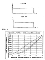
- FIGS. 3A, 3B the horizontal axes in FIG. 3 represent the lighting period (lighting progress time t) of the element in the scan period of one line, and the vertical axes represent the light emission intensity (L).
- the charging operation for the parasitic capacitance of an EL element which will be a next scan lighting object is implemented by rush current via respective parasitic capacitances in the parallel state of the other EL elements which will not be the scan lighting object.
- this charging operation is implemented utilizing a reverse bias voltage VM which is higher than a forward voltage Vf of an EL element in a lighting state, the rising of the lighting is the spike-like rising as shown in FIG. 3B.
- time gradation which controls a light emission time can be utilized suitably.
- the gradation (PWM time) vs. intensity characteristic becomes the time integral of the light emission response waveform shown in FIG. 3. Accordingly, in the case of control in which PWM is equally divided by the rectangular light emission drive as shown in FIG. 3A, a characteristic in which gradation is linear is obtained.
- the minimum intensity resolution in the gamma curve corresponds to the intensity difference between the 0th gradation and the first gradation. Accordingly, in the case where one tries to obtain a gamma characteristic by the rectangular light emission drive as shown in FIG. 3A, it is necessary to make a PWM resolution of a low gradation side small.
- Table 1 shows results of calculation of how large minimum PWM resolution is necessary taking a 16 step gradation display of the rectangular light emission drive as an example.
- Minimum resolution magnification (for gamma 1) 1.000 8.727 15.000 25.782
- the EL element has a temperature dependency as described based on FIG. 2C, and therefore changes in the light emission rising depending on temperature largely influences the gamma characteristic.
- the present invention has been developed as attention to the above-described problems has been paid, and it is an object of the present invention to provide a drive method and a drive device for a passive drive type light emitting display panel by which an excellent gradation expression can be realized without subdividing intensity resolution so much in the case where the above-mentioned time gradation is performed.
- a drive method of a light emitting display panel according to the present invention which has been developed in order to carry out the object described above is, as described in a first aspect, a drive method of a light emitting display panel in which light emitting elements are connected at respective crossing points between a plurality of data lines and a plurality of scan lines so that the light emitting elements connected to the respective scan lines are sequentially selectively lighted by sequentially scanning the scan lines, characterized in that provided is at least one of an intensity increase period in which a light emission intensity of the light emitting element is gradually increased allowing the light emission intensity to reach a constant intensity state within a predetermined period from a scan start in one scan period or an intensity decrease period in which the light emission intensity of the light emitting element is gradually decreased from the constant intensity state within a predetermined period which is immediately before the completion of the scan period.
- a drive device of a light emitting display panel according to the present invention which has been developed in order to carry out the object described above is, as described in a tenth aspect, a drive device of a light emitting display panel of a passive drive system in which light emitting elements are connected at respective crossing points between a plurality of data lines and a plurality of scan lines so that the light emitting elements connected to the respective scan lines are sequentially selectively lighted by sequentially scanning the scan lines, characterized in that provided is at least one of an intensity increase period in which a light emission intensity of the light emitting element is gradually increased allowing the light emission intensity to reach a constant intensity state within a predetermined period from a scan start in one scan period or an intensity decrease period in which the light emission intensity of the light emitting element is gradually decreased from the constant intensity state within a predetermined period which is immediately before the completion of the scan period.
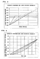
- FIG. 5 shows cases where intensity increase periods are 0 to 100% of a scan period and shows results of rough estimates for the relationships of gradations to intensities.
- the intensity can be found by time integral calculus for the light emission response, and results thereof are shown in FIG. 6.
- Respective solid line (bold line), solid line (thin line), broken line (bold line), broken line (thin line), alternate long and short dash line, and alternate long and two short dashes line shown in FIG. 5 correspond to respective those shown in FIG. 6.
- the longer the intensity increase period within the scan period the more moderate intensity increase is shown in a low PWM region as shown in FIG. 6. That is, the light emission intensity of a light emitting element can have the characteristic as the gamma curve described based on FIG. 4. As a result, a minimum time resolution can be set largely, and it becomes unnecessary to increase the clock speed.
- a drive method of a light emitting display panel according to the present invention is characterized by adopting at least either one of setting an intensity increase period at a scan start time in one scan period or setting an intensity decrease period immediately before the end of a scan period.
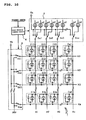
- FIG. 8 shows a passive drive type display panel developed based on the above-described technical concept and a first embodiment of a drive device thereof. Operations thereof based on the embodiment shown in FIG. 8 will be described with reference to an example in which the intensity increase period is set at a scan start time in one scan period.
- anode rays A1 to An as n data lines are arranged in a vertical direction
- cathode rays K1 to Km as m scan lines are arranged in a horizontal direction
- organic EL elements E11 to Enm as light emitting elements are arranged at portions at which respective rays intersect each other (in total, nxm portions) to constitute a display panel 1.
- One ends (anode terminals in equivalent diodes of the EL elements) and other ends (cathode terminals in the equivalent diodes of the EL elements) of the respective EL elements E11 to Enm constituting pixels are connected to the anode rays and cathode rays, respectively, corresponding to respective crossing positions between the anode rays A1 to An extending along the vertical direction and the cathode rays K1 to Km extending along the horizontal direction.
- the respective anode rays A1 to An are connected to an anode ray drive circuit 2
- the respective cathode rays K1 to Km are connected to a cathode ray scan circuit 3, so as to be driven, respectively.
- the anode ray drive circuit 2 is provided with respective constant current sources cc1 and drive switches Sa1 to San supplying drive current to the respective EL elements via the respective anode rays A1 to An.
- the drive switches Sa1 to San are connected to the respective constant current sources cc1 sides and are controlled so that current from the constant current sources cc1 is supplied to the respective EL elements E11 to Enm arranged corresponding to the cathode rays.
- the drive switches Sa1 to San are constructed so that the anode rays are selectively connected to a voltage source Va or a reference potential (a ground potential) as described later.
- the cathode ray scan circuit 3 is provided with scan switches Sk1 to Skm corresponding to the respective cathode rays K1 to Km and operates so as to allow either one of a voltage source Vk or the ground potential as a scan reference potential to be connected to corresponding cathode rays.
- a voltage source Vk or the ground potential as a scan reference potential
- the anode ray drive circuit 2 and the cathode ray scan circuit 3 receive commands from a light emission control circuit 4 and operate so as to display an image corresponding to image data, in response to said image data supplied to the light emission control circuit.
- the cathode ray scan circuit 3 sequentially selects one of the cathode rays corresponding to the horizontal scan period of the image data by a command from the light emission control circuit to set it to the ground potential as the scan reference potential and sequentially switches the scan switches Sk1 to Skm so that the voltage of the voltage source Vk is applied to other cathode rays.
- the state shown in FIG. 8 shows a state in which the second cathode ray K2 is scanned and in which the voltage of the voltage source Vk is applied to the other cathode rays.
- a drive control signal for controlling any one of the EL elements connected to the cathode rays as to which timing and how long period of time light emission is performed based on pixel information that the image data shows is supplied from the light emission control circuit 4 to the anode ray drive circuit 2.
- the anode ray drive circuit 2 instantaneously connects some of the drive switches Sa1 to San to the voltage source Va and connects them to the constant current sources cc 1 sides to control them in response to the drive control signal so as to supply drive current to EL elements corresponding to the pixel data via the anode rays A1 to An.
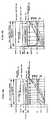
- FIG. 9A is a timing diagram explaining lighting control for the display panel operated through the first embodiment shown in FIG. 8.
- the horizontal axis shows one line of scan period in one cathode ray.
- Reference numeral 1 in the drawing shows the applied voltage for the EL elements
- reference numeral 2 shows a light emission response characteristic of the EL element, that is, the light emission intensity.
- reference numeral 3 shows the time integral value of the light emission response characteristic of the EL element shown as 2
- reference numeral 4 shows an ideal gamma curve.
- the voltage value of the voltage source Va supplied to the anode ray drive circuit 2 is set to a voltage lower than a forward voltage Vf in the light emission state (the constant intensity period) of the EL element or the above-mentioned lighting threshold voltage Vth.
- the voltage value of the voltage source Vk utilized in the cathode ray scan circuit 3 is set to a voltage higher than the forward voltage Vf.
- one means of the above-mentioned cathode reset method is adopted in the lighting control therefor.
- one means of this cathode reset method is called a voltage setting means.
- FIG. 9A at a beginning of one line scan period, the voltage of the voltage source Va is supplied to the anodes of the EL elements that are to be scan light emission objects via the anode rays. That is, the drive switches Sa1 to San in the anode ray drive circuit 2 are connected to the voltage source Va side.
- the voltage from the voltage source Vk is supplied to the cathodes of the EL elements. That is, the scan switches Sk1 to Skm in the cathode ray scan circuit 3 are connected to the voltage source Vk side. Accordingly, in this state, the voltage of "Va-Vk" is applied to the EL elements as shown as 1 in FIG. 9A.
- the drive switches Sa1 to San of the anode rays corresponding to EL elements whose lights are to be emitted are connected to the constant current sources cc1 side, and the cathode ray of the scan object is connected to the ground potential.
- electrical charges of non-scan line capacitances (usually, satisfactorily larger than capacitance components of a scan selected ray) connected to anode rays are concentrated (rush current) in the scan selected ray.
- the anode potentials become approximately the potential of Va by acceptance and delivery of electrical charges. That is, in a first set period of the scan period, setting is performed so that voltage between both ends of the EL element becomes approximately Va.
- the relationship between the PWM time and the intensity is found by the time integral of the light emission response shown by 2 as shown by 3. Accordingly, PWM periods of respective gradations can be set by the time integral of the light emission response shown by 3. Therefore, by selecting the PWM periods of the respective gradations, in other words, by setting the drive switches Sa1 to San shown in FIG. 8 to the ground potential side in response to a gradation expression, the light emission time of an EL element can be controlled, and a gradation expression by the PWM gradation method can be realized.
- the PWM periods of the respective gradations shown in FIG. 9A are set based on the light emission response characteristic shown by 2, and in the case where a further ideal gamma curve is sought, it is desired that the PWM time is adjusted on the time axis for each gradation by calculating back from an intensity value of the ideal gamma curve shown by 4. Thus, a gradation corresponding to the ideal gamma curve can be obtained.
- FIG. 9B illustrates PWM periods of respective gradations performed in a conventional example having a light emission characteristic as shown in FIG. 3 which has already been described. Respective characteristics shown by 1 to 4 in FIG. 9B are similar to those described in FIG. 9A. That is, in the conventional method, the relationship between the anode side voltage Va and the forward voltage Vf is set to Va ⁇ Vf, and therefore the rising of light emission of an EL element is rectangular or spike-like.
- FIG. 10 shows a second embodiment of a drive device according to the present invention.
- parts corresponding to the respective constituent parts shown in FIG. 8 which has already been described are shown by the same reference numerals, and thus detailed explanation thereof will be omitted. Operations thereof based on the embodiment shown in FIG. 10 will be described in accordance with an example in which an intensity increase period is set at a scan start time within one scan period.
- respective first constant current sources cc1 for the light emission risings of EL elements and second constant current sources cc2 for performing the light emission in a constant intensity state are provided in the anode ray drive circuit 2.
- the voltage value of the voltage source Va supplied to the anode ray drive circuit 2 is set at a voltage lower than the above-mentioned lighting threshold voltage Vth.
- the voltage value of the voltage source Vk utilized in the cathode ray scan circuit 3 is set at a voltage higher than the forward voltage Vf.
- FIG. 11 is for explaining lighting control of the display panel performed by the second embodiment shown in FIG. 10. That is, FIG. 11A is for explaining the circumstances of the light emission rising of an EL element performed first in each one line scan period, and FIG. 11B is a timing diagram explaining the lighting control for the display panel.
- FIG. 11B similarly to the example shown in FIG. 9, the horizontal axis thereof shows one line of scan period in one cathode ray.
- the timing diagram shown in FIG. 11A explains a charging operation for an element at a beginning of one line scan period in FIG. 11B, that is, the part enclosed by broken lines.
- reference numeral 1 shows the applied voltage for the EL element
- 2 shows a light emission response characteristic of the EL element, that is, the light emission intensity
- 3 shows the time integral value of the light emission response characteristic of the EL element shown as the 2
- 4 shows an ideal gamma curve.
- the drive switches Sa1 to San have already been connected to the voltage source Va at a scan finishing time of a line before said line.
- a scan cathode ray is connected to the ground potential, and non-scan cathode rays are connected to the voltage source Vk.
- the applied voltage to the respective EL elements that are to be scanned are allowed to be Va. That is, in the set period that is a beginning of the scan period, the voltage of both ends of the EL element is set to approximately Va, and here they function as a voltage setting means for setting the both end voltage of the EL element to a constant voltage value.
- the drive switches Sa1 to San are connected to the first constant current sources cc1 sides which are for light emission rising.
- FIG. 11A shows an equivalent circuit regarding one anode ray at this time, meaning a structure in which one EL element to be a scan object for the constant current source cc1 and a plurality of EL elements to be non-scan objects are connected in parallel and in which n parasitic capacitances C in total are connected. Charging operation is performed through the constant current source cc1 for the parasitic capacitances of the respective EL elements. At this time electrical charges corresponding to Va have already been charged in the parasitic capacitances C of the respective EL elements as described above.
- the reference numeral 3 in FIG. 11B is the time integral of the light emission response shown by 2, and thus the PWM periods of the respective gradations can be set.
- the drive switches Sa1 to San shown in FIG. 10 are set to the Va side in response to a gradation expression so that the light emission time of the EL element can be controlled, and a gradation expression by the PWM gradation method can be realized.
- the PWM time can be adjusted on the time axis for each gradation by calculating back from an intensity value of the ideal gamma curve shown by 4, and thus a gradation corresponding to the ideal gamma curve can be obtained.
- the terminal voltages of EL elements are increased utilizing the constant current sources cc1 at a beginning of one scan period
- a constant voltage source by which voltage gradually increases in the intensity increase period may be employed instead of the constant current source cc1.
- the intensity increase period can be formed at a beginning of one scan period, and similar interactions and effects can be obtained.
- the applied voltage to the light emitting element at the time of completion of the intensity increase period is set at a voltage value which is approximately equal to the forward voltage Vf of the light emitting element in the constant intensity state.
- a constant voltage source by which voltage gradually increase is employed instead of the constant current source cc1 shown in FIG. 10 so that through at least one of voltage sweep widths (time length, current value, voltage value) and the like, a drive operation which differs depending on respective colors can be performed.
- a drive operation which differs depending on respective colors can be performed as described above, the intensity from a low gradation to a high gradation of an organic EL element which emits respective colors of light and white balance can be adjusted, whereby an excellent gamma characteristic can be obtained.
- Such intensity decrease period can be realized by a setting in which the current value supplied to a light emitting element in a constant intensity state differs from the current value supplied to the light emitting element in the intensity decrease period. Further, a constant voltage source by which the voltage gradually decreases in the intensity decrease period may be employed.
- the applied voltage to the light emitting element at the start time of the intensity decrease period is set at a voltage value which is approximately equal to the forward voltage Vf of the light emitting element in the constant intensity state.
Landscapes
- Engineering & Computer Science (AREA)
- Physics & Mathematics (AREA)
- Computer Hardware Design (AREA)
- General Physics & Mathematics (AREA)
- Theoretical Computer Science (AREA)
- Control Of Indicators Other Than Cathode Ray Tubes (AREA)
- Electroluminescent Light Sources (AREA)
- Control Of El Displays (AREA)
Applications Claiming Priority (2)
| Application Number | Priority Date | Filing Date | Title |
|---|---|---|---|
| JP2003093812 | 2003-03-31 | ||
| JP2003093812A JP2004302025A (ja) | 2003-03-31 | 2003-03-31 | 発光表示パネルの駆動方法および駆動装置 |
Publications (1)
| Publication Number | Publication Date |
|---|---|
| EP1465144A2 true EP1465144A2 (de) | 2004-10-06 |
Family
ID=32844606
Family Applications (1)
| Application Number | Title | Priority Date | Filing Date |
|---|---|---|---|
| EP04004689A Withdrawn EP1465144A2 (de) | 2003-03-31 | 2004-03-01 | Steuerverfahren und Vorrichtung zur Pulsbreitenmodulation für eine elektrolumineszente Anzeigevorrichtung |
Country Status (6)
| Country | Link |
|---|---|
| US (1) | US20040189558A1 (de) |
| EP (1) | EP1465144A2 (de) |
| JP (1) | JP2004302025A (de) |
| KR (1) | KR20040086181A (de) |
| CN (1) | CN1534575A (de) |
| TW (1) | TWI240903B (de) |
Cited By (2)
| Publication number | Priority date | Publication date | Assignee | Title |
|---|---|---|---|---|
| EP2107547A3 (de) * | 2008-04-01 | 2010-05-05 | Canon Kabushiki Kaisha | Bildanzeigevorrichtung und Steuerverfahren dafür |
| US8810555B2 (en) | 2009-09-02 | 2014-08-19 | Scobil Industries Corp. | Method and apparatus for driving an electroluminescent display |
Families Citing this family (11)
| Publication number | Priority date | Publication date | Assignee | Title |
|---|---|---|---|---|
| JP2004302070A (ja) * | 2003-03-31 | 2004-10-28 | Tohoku Pioneer Corp | 発光表示パネルの駆動装置 |
| JP2006039039A (ja) * | 2004-07-23 | 2006-02-09 | Tohoku Pioneer Corp | 自発光表示パネルの駆動装置、駆動方法及びその駆動装置を備えた電子機器 |
| JP4743685B2 (ja) * | 2005-01-06 | 2011-08-10 | 東北パイオニア株式会社 | 発光表示パネルの駆動装置および駆動方法 |
| JP5064696B2 (ja) | 2006-02-16 | 2012-10-31 | ラピスセミコンダクタ株式会社 | 表示パネルの駆動装置 |
| TWI346922B (en) * | 2006-06-14 | 2011-08-11 | Au Optronics Corp | Structure of pixel circuit for display and mothod of driving thereof |
| US20080150839A1 (en) * | 2006-12-20 | 2008-06-26 | Kazuyoshi Kawabe | Controlling light emission in display device |
| GB2453375A (en) * | 2007-10-05 | 2009-04-08 | Cambridge Display Tech Ltd | Driving a display using an effective analogue drive signal generated from a modulated digital signal |
| JP5630210B2 (ja) * | 2010-10-25 | 2014-11-26 | セイコーエプソン株式会社 | 画素回路の駆動方法、電気光学装置および電子機器 |
| KR102088683B1 (ko) * | 2015-09-04 | 2020-03-13 | 삼성전자주식회사 | 영상표시장치 및 영상표시장치의 구동 방법 |
| CN111063289B (zh) * | 2019-12-25 | 2022-08-02 | Tcl华星光电技术有限公司 | 灰阶补偿方法、装置及显示设备 |
| CN114080085B (zh) * | 2020-08-20 | 2025-04-11 | 群创光电股份有限公司 | 发光装置 |
Family Cites Families (2)
| Publication number | Priority date | Publication date | Assignee | Title |
|---|---|---|---|---|
| US6803890B1 (en) * | 1999-03-24 | 2004-10-12 | Imaging Systems Technology | Electroluminescent (EL) waveform |
| JP3850241B2 (ja) * | 2001-07-19 | 2006-11-29 | シャープ株式会社 | 照明装置およびそれを用いた液晶表示装置 |
-
2003
- 2003-03-31 JP JP2003093812A patent/JP2004302025A/ja not_active Withdrawn
-
2004
- 2004-02-27 TW TW093105135A patent/TWI240903B/zh not_active IP Right Cessation
- 2004-03-01 EP EP04004689A patent/EP1465144A2/de not_active Withdrawn
- 2004-03-01 US US10/788,465 patent/US20040189558A1/en not_active Abandoned
- 2004-03-19 KR KR1020040018992A patent/KR20040086181A/ko not_active Withdrawn
- 2004-03-31 CN CNA2004100332304A patent/CN1534575A/zh active Pending
Cited By (3)
| Publication number | Priority date | Publication date | Assignee | Title |
|---|---|---|---|---|
| EP2107547A3 (de) * | 2008-04-01 | 2010-05-05 | Canon Kabushiki Kaisha | Bildanzeigevorrichtung und Steuerverfahren dafür |
| US8259140B2 (en) | 2008-04-01 | 2012-09-04 | Canon Kabushiki Kaisha | Method of controlling an image display apparatus |
| US8810555B2 (en) | 2009-09-02 | 2014-08-19 | Scobil Industries Corp. | Method and apparatus for driving an electroluminescent display |
Also Published As
| Publication number | Publication date |
|---|---|
| US20040189558A1 (en) | 2004-09-30 |
| KR20040086181A (ko) | 2004-10-08 |
| JP2004302025A (ja) | 2004-10-28 |
| TW200424991A (en) | 2004-11-16 |
| CN1534575A (zh) | 2004-10-06 |
| TWI240903B (en) | 2005-10-01 |
Similar Documents
| Publication | Publication Date | Title |
|---|---|---|
| US6965362B1 (en) | Apparatus and method for driving light emitting panel | |
| KR100432173B1 (ko) | 유기el표시장치 및 그 구동방법 | |
| JP3874390B2 (ja) | 容量性発光素子ディスプレイ装置及びその駆動方法 | |
| JP3613451B2 (ja) | 多色発光表示パネルの駆動装置及び駆動方法 | |
| JP3737889B2 (ja) | 発光ディスプレイ装置および駆動方法 | |
| US8125479B2 (en) | Self light emitting type display device | |
| EP1486943A2 (de) | Vorrichtung und Verfahren zur Ansteuerung eines Licht emittierenden Anzeige-Paneels | |
| US6774878B2 (en) | Drive unit for a luminescence display panel | |
| US6339415B2 (en) | Electroluminescent display and drive method therefor | |
| US6771235B2 (en) | Apparatus and method for driving display panel | |
| JPH11143429A (ja) | 発光ディスプレイ及びその駆動方法 | |
| EP1465144A2 (de) | Steuerverfahren und Vorrichtung zur Pulsbreitenmodulation für eine elektrolumineszente Anzeigevorrichtung | |
| US20020190934A1 (en) | Drive unit for a luminescence display panel | |
| US20050052448A1 (en) | Drive device and drive method of light emitting display panel | |
| US7038393B2 (en) | Drive device for light-emitting display panel | |
| US6229267B1 (en) | Display apparatus with capacitive light-emitting devices and method of driving the same | |
| JP3552150B2 (ja) | カラー表示装置 | |
| CN100385489C (zh) | 发光显示面板的驱动装置 | |
| JP2001042824A (ja) | 多色発光表示パネルの駆動装置 | |
| JP4988300B2 (ja) | 発光素子及びその駆動方法 | |
| US7119763B2 (en) | Light emitting circuit for organic electroluminescence element and display device | |
| JP2000148086A (ja) | 発光ディスプレイ装置および駆動方法 | |
| JP2003228326A (ja) | 有機エレクトロルミネッセンス素子の発光回路及び表示装置 |
Legal Events
| Date | Code | Title | Description |
|---|---|---|---|
| PUAI | Public reference made under article 153(3) epc to a published international application that has entered the european phase |
Free format text: ORIGINAL CODE: 0009012 |
|
| AK | Designated contracting states |
Kind code of ref document: A2 Designated state(s): AT BE BG CH CY CZ DE DK EE ES FI FR GB GR HU IE IT LI LU MC NL PL PT RO SE SI SK TR |
|
| AX | Request for extension of the european patent |
Extension state: AL LT LV MK |
|
| PUAL | Search report despatched |
Free format text: ORIGINAL CODE: 0009013 |
|
| STAA | Information on the status of an ep patent application or granted ep patent |
Free format text: STATUS: THE APPLICATION HAS BEEN WITHDRAWN |
|
| PUAF | Information related to the publication of a search report (a3 document) modified or deleted |
Free format text: ORIGINAL CODE: 0009199SEPU |
|
| 18W | Application withdrawn |
Effective date: 20070921 |
|
| AK | Designated contracting states |
Kind code of ref document: A3 Designated state(s): AT BE BG CH CY CZ DE DK EE ES FI FR GB GR HU IE IT LI LU MC NL PL PT RO SE SI SK TR |
|
| AX | Request for extension of the european patent |
Extension state: AL LT LV MK |
|
| D17D | Deferred search report published (deleted) |