EP1465409B1 - Capteur d'image, procédé pour le commander et caméra - Google Patents
Capteur d'image, procédé pour le commander et caméra Download PDFInfo
- Publication number
- EP1465409B1 EP1465409B1 EP04008125A EP04008125A EP1465409B1 EP 1465409 B1 EP1465409 B1 EP 1465409B1 EP 04008125 A EP04008125 A EP 04008125A EP 04008125 A EP04008125 A EP 04008125A EP 1465409 B1 EP1465409 B1 EP 1465409B1
- Authority
- EP
- European Patent Office
- Prior art keywords
- image sensor
- signal
- selection signal
- transistor
- horizontal scanning
- Prior art date
- Legal status (The legal status is an assumption and is not a legal conclusion. Google has not performed a legal analysis and makes no representation as to the accuracy of the status listed.)
- Expired - Lifetime
Links
Images





Classifications
-
- H—ELECTRICITY
- H04—ELECTRIC COMMUNICATION TECHNIQUE
- H04N—PICTORIAL COMMUNICATION, e.g. TELEVISION
- H04N25/00—Circuitry of solid-state image sensors [SSIS]; Control thereof
- H04N25/70—SSIS architectures; Circuits associated therewith
- H04N25/76—Addressed sensors, e.g. MOS or CMOS sensors
- H04N25/77—Pixel circuitry, e.g. memories, A/D converters, pixel amplifiers, shared circuits or shared components
-
- H—ELECTRICITY
- H04—ELECTRIC COMMUNICATION TECHNIQUE
- H04N—PICTORIAL COMMUNICATION, e.g. TELEVISION
- H04N25/00—Circuitry of solid-state image sensors [SSIS]; Control thereof
- H04N25/50—Control of the SSIS exposure
- H04N25/53—Control of the integration time
-
- H—ELECTRICITY
- H04—ELECTRIC COMMUNICATION TECHNIQUE
- H04N—PICTORIAL COMMUNICATION, e.g. TELEVISION
- H04N25/00—Circuitry of solid-state image sensors [SSIS]; Control thereof
- H04N25/70—SSIS architectures; Circuits associated therewith
- H04N25/71—Charge-coupled device [CCD] sensors; Charge-transfer registers specially adapted for CCD sensors
- H04N25/74—Circuitry for scanning or addressing the pixel array
-
- H—ELECTRICITY
- H04—ELECTRIC COMMUNICATION TECHNIQUE
- H04N—PICTORIAL COMMUNICATION, e.g. TELEVISION
- H04N25/00—Circuitry of solid-state image sensors [SSIS]; Control thereof
- H04N25/70—SSIS architectures; Circuits associated therewith
- H04N25/76—Addressed sensors, e.g. MOS or CMOS sensors
- H04N25/779—Circuitry for scanning or addressing the pixel array
Definitions
- the present invention relates to an image sensor comprising a sensor unit that is made up of a plurality of pixels and a plurality of scanning circuits, each of which has a dynamic logic circuit for outputting, with the use of different scanning methods, an output signal for selecting a row or a column in the sensor unit.
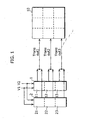
- the conventional image sensor as such that is published in Japanese Laid-Open Application No. JP-A-2003-46879 has, as shown in FIG. 1, a sensor unit 10 and a plurality of scanning circuits 1, 2 so as to realize, for example, an electronic shutter function.
- the scanning circuits 1 and 2 are shift registers, each of which is composed of plural stages of unit registers, and output, to the sensor unit 10, an output signal for reading out a pixel signal at an independent timing.
- the output is a wire connected electrically.
- the electronic shutter function of the image sensor is to adjust a charge storage time of the image sensor by means of its drive, and control electrically an exposure time instead of a physical function of aperture.
- the electronic shutter function can be achieved by resetting a signal charge accumulated in each of the pixels at a timing different from that of reading out the pixel signal.
- the scanning circuit 1 outputs a row selection signal to be used for reading out a normal pixel signal while the scanning circuit 2 outputs a row selection signal to be used for resetting operated by the electronic shutter function.
- the signals V1 and V2 are two-phase clock signals, on which shifting operation bases.
- the clock signal V1 is inputted into the unit registers arranged in "2N+1" th (where N is an integer) stages while the clock signal V2 is inputted into the unit registers arranged in "2N" th stages.
- N is an integer
- the Transout 1 signal is outputted as a logical OR of two output signals outputted from the unit register at the first stage in the scanning circuits 1 and 2.
- the Transout 2 and 3 signals are outputted in the same manner as the Transout 1, but the unit registers to which they respectively correspond are different.
- FIG. 2B shows an operation performed by the unit register in a case where the input signal In is at high level. Since the input signal In is at high level, a gate electrode of the transistor Tr4 is already at high level due to a gate capacitor of the transistor Tr4 and a potential of the capacitor C1, before the rising edge of the clock signals V1/V2 (1 in the diagram). In this state, when the clock signals V1/V2 rise from low level to high level, a gate voltage In in the transistor Tr4 is boosted via the capacitor C1 (2 in the diagram).
- the potential under a gate becomes higher than a high level of the clock signals V1/V2 since a voltage higher than the high level of the clock signals V1/V2 is applied to the gate of the transistor Tr4, and thereby, the Out signal is outputted at the level as high as that of the clock signals V1/V2 (3 in the diagram).
- the Out signal is outputted at the level as low as that of the clock signals V1/V2.
- the Next signal is outputted at high level even after the fall of the clock signals V1/V2 since the high level is maintained in the gate capacitor of the transistor Tr5 that is unidirectional.
- the reason why the respective outputs from the unit registers in the scanning circuits 1, 2 are wire connected is that the output lines, other than the one outputting a selection signal at high level, are in a state of floating, in the case where the scanning circuits 1, 2 are respectively composed of shift registers operated using the NMOS dynamic logic circuit.
- the logical OR of the outputs can be obtained via the wire connection.
- the image sensor has a structure in which the plural scanning circuits with different scanning directions are arranged and an access signal for scanning vertically or horizontally is outputted to the sensor unit 10 by wire connecting the outputs electrically.
- the scanning circuit 1 outputs the row selection signal used for reading out a normal pixel signal while the scanning circuit 2 outputs the row selection signal used for inversely reading out in order to scan in a reverse direction.
- the image sensor having plural shift registers, each of which has the NMOS dynamic logic circuit contains the following problem.
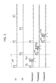
- the V1, V2 are the two-phase clock signals while Transout1 ⁇ 3 are signals respectively outputted to the sensor unit in correspondence with the first through third stages.
- the pulse P1 of the Transout 1 signal is generated when the clock signal V1 itself is outputted via the transistor Tr4.
- the pulse P2 of the Transout 2 signal is generated when the clock signal V2 itself is outputted via the transistor Tr4 (in FIG. 2).
- the Transout 3 signal and the Transout signals,corresponding to the following stages are operated in the same manner.
- a timing to output the pulse of the Transout signal is fixed as in the case of the timing to output the pulse of the clock signal. It is therefore a problem that a Transout signal for electronic shutter use cannot be outputted at an arbitrary timing, for instance, the timings of P11, P22 and P33 shown in the diagram, within one horizontal period of time (1H in the diagram).
- An object of the present invention in view of the above problem, is to provide the image sensor which has a scanning circuit for electronic shutter use, for outputting an output signal in order to select pixels in a row or in a column of the sensor unit using a dynamic logic circuit, and can output the output signal at an arbitrary timing during a horizontal scanning period, a driving method thereof and a camera therewith.
- the image sensor according to the present invention in order to achieve the above object comprise: a sensor unit that is made up of a plurality of pixels; a scanning circuit having a dynamic logic circuit for outputting selection signals that select pixels from among said plurality of pixels in the sensor unit; and a bootstrap circuit placed between the scanning circuit and the sensor unit, for holding a selection signal outputted from the scanning circuit during one horizontal scanning period, and outputting, to the sensor unit, an AND signal obtained by performing a logical AND between the held selection signal and a drive signal that specifies a timing to output the AND signal to the sensor unit.
- the selection signal outputted from the scanning circuit is held during one horizontal scanning period so that the timing to apply the drive signal that specifies the timing to output the AND signal to the sensor unit can be arbitrary within the horizontal scanning period, without restriction.
- the AND signal can be outputted as a pixel selection signal that is, for instance, for electronic shutter use.
- the bootstrap circuit may include: a switch connected to a selection signal line from the scanning circuit; a boosting transistor for holding said selection signal in a gate capacitor; and a capacitative element for boosting a gate voltage in the boosting transistor, wherein the boosting transistor holds said selection signal in the gate capacitor by an input of said selection signal to a gate of the boosting transistor via the switch, and outputs said AND signal from one of either drain or source to the sensor unit by an input of said drive signal to the other of the drain or source.
- the selection signal outputted from the scanning circuit may be at high level during said one horizontal scanning period even while the gate capacitor holds said selection signal. In this case, the scanning circuit outputs said selection signal at high level during said one horizontal scanning period by use of a drive pulse that is at high level during said one horizontal scanning period.
- the switch may be also a switching transistor, and a threshold of the gate voltage to turn on the switching transistor is smaller than a threshold of the gate voltage to turn on the boosting transistor.
- the boosting transistor sets a high threshold so as to continue to shield the drive signal until the high level signal is boosted in the gate, while the switching transistor sets a low threshold so that the boosting transistor is easily switched on by the selection signal outputted from the scanning circuit. Consequently, this structure is practical to lower the power supply in the image sensor. Namely, the low voltage operations with small voltage margin can be realized.
- the switch may transmit said selection signal to the gate of the boosting transistor when said switch is turned on at a time when one horizontal scanning period shifts to another horizontal scanning period.
- the scanning circuit may output said selection signal as a pulse having an arbitrary width during said one horizontal scanning period, by use of a drive pulse having said arbitrary width.
- the switch may also be a switching transistor that is always on, and the scanning circuit outputs said selection signal as a pulse having an arbitrary width during said one horizontal scanning period, by use of a drive pulse having said arbitrary width.
- the boosting transistor is boosted by the drive signal when the selection signal is at high level.
- the threshold of the switching transistor can be therefore reduced even more, which enables a low power supply in the image sensor.
- the capacitative element is a gate capacitor of an enhancement-typed transistor in which the drain and the source are short-circuited.
- the boosting operation performed by the boosting transistor can be controlled more surely, in the case where the output signal outputted from the scanning circuit is at low level.
- the timing to apply the drive signal for electronic shutter use can be arbitrary within one horizontal scanning period of time without any restriction and the pixel selection signal for electronic shutter use can be arbitrary within one horizontal scanning period of time.
- the image sensor is applicable for low voltage in the power supply, that is to say, low voltage operation with less voltage margin is made possible. In this way, the boosting operation in the boosting transistor can be surely controlled in the case where the output signal ,outputted from the scanning circuit is at low level.
- the embodiments of the present invention describe an image sensor which is incorporated in a cell phone, a Personal Digital. Assistant or a camera.
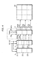
- FIG. 4 is a sketchy diagram showing the main part of the image sensor according to the first embodiment of the present invention.
- the image sensor is composed of: a scanning circuit 1 for performing normal scanning; a scanning circuit 2 for performing scanning for electronic shutter use; a selection circuit 3 for selecting an output signal outputted from the scanning circuits 1, 2, and outputting it at an arbitrary timing; and the sensor unit 10 being made up of a plurality of pixels.
- the scanning circuits 1, 2 and the sensor unit 10 are as same as those described in FIG. 1 and the structure of the unit register constituting the scanning circuits 1, 2 is as same as the one described in FIG. 2A, therefore, the descriptions are omitted here.
- the TRANS and ETRANS signals in FIG. 1 are control signals for specifying the output signal outputted from the scanning circuits 1, 2 as well as the timing to output the output signal.
- the selection circuit 3 holds the output signal Out outputted from the scanning circuit 1 and outputs the held output signal Out as a TRANSOut signal at a pulse timing of the TRANS signal.
- the selection circuit 3 also holds the output signal EOut outputted from the scanning circuit 2 and outputs the held EOut signal as a TRANSOut signal at a pulse timing of the held EOut signal.
- the selection circuit is composed of a plurality of unit selection circuits (the part surrounded with a dotted line is a unit selection circuit 31). Each of the unit selection circuits outputs selectively, at the pulse timing of the TRANS, ETRANS signals, either the output signals Out or EOut which are outputted from the scanning circuits 1, 2.
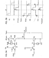
- FIG. 5A is a circuit diagram showing the structure of the unit selection circuit 31.
- the unit selection circuit is composed of two bootstrap circuits, for holding the output signal EOut outputted from the unit register 21 in the scanning circuit 2 as well as the output signal Out outputted from the unit register 11 in the scanning circuit 1 and outputting selectively one of the held signals.
- the bootstrap circuit adapted for the output signal EOut is composed of a switching transistor Tr1E for controlling an input of the output signal EOut, a boosting transistor Tr2E for holding the inputted output signal, and an enhancement-typed transistor Tr3E as a boost capacitor.
- the bootstrap circuit adapted for the output signal Out is composed of the transistors Tr1, Tr2 and Tr3.
- the enhancement-typed transistor Tr3E as a boost capacitor connects a source with a drain so as to connect them with the ETrans signal line and connects a gate with the gate of the boosting transistor Tr2E.
- the enhancement-typed transistor is characterized by its operation: it does not function as a boost capacitor without conduction when a gate voltage is less than or equal to the threshold, but functions as such when the gate voltage goes beyond the threshold.
- the output signal EOut outputted from the unit register 21 becomes synchronous with the clock signal V1 and rises to high level (1 in the diagram).
- the clock signal being at high level
- the switching transistor Tr1E is ON and the output signal EOut at high level is inputted to the gate of the boosting transistor Tr2E via the switching transistor Tr1E.
- the gate capacitor of the boosting transistor Tr2E holds the inputted high level signal and continues to hold the high level signal (hereinafter to be referred to as EIn signal), even after the clock signal Clk falls to low level and the switching transistor Tr1E is OFF.
- the EIn signal is at high level mostly through one horizontal scanning period (1H) until the clock signal Clk is ON and the level of the gate electrode of the boosting transistor Tr2E is made low.
- the boosting transistor Tr2E Since the boosting transistor Tr2E is ON and the ETrans signal is at high level within one horizontal scanning period (2 in the diagram) due to the EIn signal, the EIn signal is boosted by a voltage higher than the level of the EIn signal via the gate capacitor of the enhancement-typed transistor Tr3E, and the pulse of the ETrans signal is outputted as a Transout signal via the boosting transistor Tr2E (4 in the diagram).
- the switching transistor Tr1E is switched ON, the gate electrodes of the boosting transistor Tr2E and the enhancement-typed transistor Tr3E fall to low level due to the EOut signal at low level, and then the EIn signal is reset (low level).
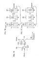
- FIG. 6A shows a half of the structure in the unit selection circuit while FIG. 6B is a time chart showing the operational timings carried out in the unit selection circuits 31, 32.
- the Eout1 and EOut2 in the diagram are the output signals outputted from the unit registers 21, 22 for the respective unit selection circuits 31, 32.
- the EIn1 and EIn2 indicate respectively a potential of the gate capacitor of the boosting transistor Tr2E in the respective unit selection circuits 31, 32.
- the pulse of the ETrans signal can be applied at an arbitrary timing within one horizontal scanning period.
- the ETrans signal (2 in the diagram) is a selection control signal for controlling the output of the output signal EOut from the scanning circuit 2 as well as for setting an arbitrary timing to output the ETransout signal (3 in the diagram) as a selection signal for the sensor unit 10.
- the timing to output the pulse of the ETransout signal is not restricted to any position on the dotted line, but may be any position on the actual line. Thus, it is possible to operate an electronic shutter within one horizontal scanning period.
- the threshold of the gate voltage for turning on the transistors Tr2E and Tr1E can be the same voltage as the power supply.
- the power supply is low (e.g., 3V, 2.5V, or the like) as in the case where the image sensor is mounted on a cell phone or the like, the voltage margin is small. It is therefore desirable that the threshold of the boosting transistor Tr2E is high while the threshold of the switching transistor Tr1E is low.
- FIGs 7A ⁇ 7C are illustrations to show a threshold for the operation where low voltage is applied.
- the ETransout signal of the boosting transistor Tr2E is outputted mistakenly during the accumulation of the signals operated by the sensor unit 10, a non-selection pixel is selected as a result. Due to this, the pixel signals which are presently accumulated fail to be accumulated, and thereby, picture quality is degraded. It is therefore desirable that the boosting transistor Tr2E has a high threshold so as to shield the ETrans signal until the high level signal that is high enough is inputted to the gate.
- FIGs 7B and 7C are pattern diagrams respectively showing the potential of the switching transistor Tr1E.
- FIG. 7C shows the case where the threshold is too low compared to FIG. 7B.
- the case of using a power supply of 2.8 V is described.
- FIGs 7B and 7C show respectively a pattern of the potential when the clock signal Clk changes from high level to low level (4 ⁇ 1 ⁇ 2 shown in the diagram).
- the operation of the switching transistor Tr1E is OFF (not ON between the source and the drain), therefore, the boosting operation can be performed (1 2 in the diagram).
- the boosting transistor Tr2E has a high threshold while the switching transistor Tr1E has a low threshold within the range where the boosting operation can be performed.
- the selection signal can be outputted, to the sensor unit 10, for the use of electrical shutter at an arbitrary timing within one horizontal scanning period. Also, low voltage in the power supply can be attempted by setting the threshold of the boosting transistor Tr2E as the one higher than that of the switching transistor Tr1E.
- the present embodiment will describe the image sensor which overcomes the problem caused by the threshold of the switching transistor Tr1E that is too low, as mentioned in the first embodiment.
- the structure of the image sensor is as same as the one shown in FIG. 4 and the structure of the unit selection circuit is as same as the one shown in FIG. 5A so that the descriptions are omitted here.
- the image sensor according to the present embodiment differs from the one described in the first embodiment in the respect that the pulse duration of the clock signals V1 and V2 are widened to make up a great part of one horizontal period.
- the output signal EOut at high level is held in the gate capacitor of the boosting transistor Tr2E at the timing shown in 1.
- the voltage is applied to the pulse ETrans so that the output signal EOut is outputted at the timing shown in 2.
- the source and drain of the switching transistor Tr1E are not ON completely. This enables the boosting operation in the boosting transistor Tr2E, and the selection signal Transout is outputted to the sensor unit 10.
- FIGs 9A ⁇ 9C are illustrations showing a threshold in the case of low-voltage operation. It is desirable that the boosting transistor Tr2E has a high threshold as shown in FIGs 7A ⁇ 7C.
- FIGs 9B and 9C are pattern diagrams showing respectively the potential of the switching transistor Tr1E in the case where the threshold is lower in FIG. 9C than in FIG. 9B.
- the switching transistor Tr1E is OFF (not ON between the source and the drain) so that the boosting operation can be performed (1 2 in the diagram).
- the selection signal for electronic shutter use can be outputted, to the sensor unit 10, at an arbitrary timing within one horizontal scanning period. Also, low power supply voltage can be facilitated by setting the threshold of the boosting transistor Tr2E higher than the threshold of the switching transistor Tr1E.
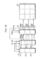
- FIG. 10 is a diagram showing the sketchy structure of the main part of the image sensor according to the third embodiment.
- the structure shown in the diagram is different from the one shown in FIG. 4 in the respect that it includes a selection circuit 3a instead of the selection circuit 3.
- the selection circuit 3a does not require the clock signal Clk, which is different from the selection circuit 3a. The following focuses on the difference and the description for the same components is omitted.
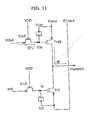
- FIG. 11 is a circuit diagram showing the structure of the selection circuit 3a.
- the power supply VDD instead of the clock signal Clk, is connected to the gate of the switching transistor Tr1E.
- FIGs 12A ⁇ 12C are illustrations showing the operation of the selection circuit 3a.
- the pulse durations of the clock signals V1, V2 are widened to make up a great part of one horizontal scanning period. It thus solves the problem that the boosting cannot be operated in the switching transistor Tr1E because the threshold is too low, as shown in FIG. 12C.
- each of the embodiments describes the case of using two scanning circuits, but the number of the circuits can be more than or equal to three.
- a bootstrap circuit may be placed for each of the output signals outputted from plural scanning circuits, and the respective outputs from each of the bootstrap circuits are connected to be outputted to the sensor unit 10, as a selected output signal.
Landscapes
- Engineering & Computer Science (AREA)
- Multimedia (AREA)
- Signal Processing (AREA)
- Transforming Light Signals Into Electric Signals (AREA)
- Solid State Image Pick-Up Elements (AREA)
Claims (19)
- Capteur d'image comprenant :une unité de capteur (10) qui est constituée d'une pluralité de pixels,un circuit de balayage (1, 2) ayant un circuit logique dynamique afin de former en sortie des signaux de sélection qui sélectionnent des pixels parmi ladite pluralité de pixels dans l'unité de capteur, etun circuit d'amorçage (3) placé entre le circuit de balayage (1, 2) et l'unité de capteur (10), afin de maintenir un signal de sélection fourni en sortie à partir du circuit de balayage durant une période de balayage horizontal, et fournir, en sortie, à l'unité de capteur, un signal ET obtenu en exécutant une opération ET logique entre le signal de sélection maintenu et un signal d'attaque qui spécifie un instant pour fournir en sortie le signal ET à l'unité de capteur,où le circuit d'amorçage (3) comprend :un commutateur (Tr1E) connecté à une ligne de signal de sélection provenant du circuit de balayage (1, 2),un transistor d'amplification (Tr2E) destiné à maintenir ledit signal de sélection dans un condensateur de grille, etun élément capacitif (Tr3E) destiné à amplifier une tension de grille dans le transistor d'amplification (Tr2E),où le transistor d'amplification (Tr2E) maintient ledit signal de sélection dans le condensation de grille par une entrée dudit signal de sélection à une grille du transistor d'amplification (Tr2E) par l'intermédiaire du commutateur (Tr1E), et fournit en sortie ledit signal ET à partir de l'un du drain ou de la source à l'unité de capteur (10) par une entrée dudit signal d'attaque vers l'autre du drain ou de la source.
- Capteur d'image selon la revendication 1,
dans lequel le signal d'attaque est destiné à une utilisation d'obturateur électronique. - Capteur d'image selon la revendication 1,
dans lequel ledit signal de sélection fourni en sortie à partir du circuit de balayage est à un niveau haut durant ladite une période de balayage horizontal même lorsque le condensateur de grille maintient ledit signal de sélection. - Capteur d'image selon la revendication 3,
dans lequel le circuit de balayage fournit en sortie ledit signal de sélection à un niveau haut durant ladite une période de balayage horizontal par l'utilisation d'une impulsion d'attaque qui est à un niveau haut durant ladite une période de balayage horizontal. - Capteur d'image selon la revendication 4,
dans lequel le commutateur est un transistor de commutation, et
un seuil de la tension de grille pour rendre conducteur le transistor de commutation est inférieur à un seuil de la tension de grille pour rendre conducteur le transistor d'amplification. - Capteur d'image selon la revendication 5,
dans lequel le commutateur transmet ledit signal de sélection à la grille du transistor d'amplification lorsque ledit commutateur est fermé à un moment où une période de balayage horizontal passe à une autre période de balayage horizontal. - Capteur d'image selon la revendication 6,
dans lequel le commutateur est un transistor de commutation qui est toujours conducteur, et
le circuit de balayage fournit en sortie ledit signal de sélection sous la forme d'une impulsion ayant une largeur arbitraire durant ladite une période de balayage horizontal, par le biais de l'utilisation d'une impulsion d'attaque ayant ladite largeur arbitraire. - Capteur d'image selon la revendication 7,
dans lequel l'élément capacitif est un condensateur de grille d'un transistor du type à enrichissement dans lequel le drain et la source sont placés en court-circuit. - Capteur d'image selon la revendication 3,
dans lequel le commutateur est un transistor de commutation, et
un seuil de la tension de grille pour rendre conducteur le transistor de commutation est inférieur à un seuil de la tension de grille pour rendre conducteur le transistor d'amplification. - Capteur d'image selon la revendication 3,
dans lequel le commutateur transmet ledit signal de sélection à la grille du transistor d'amplification lorsque ledit commutateur est fermé à un instant où une période de balayage horizontal passe à une autre période de balayage horizontal. - Capteur d'image selon la revendication 3,
dans lequel le circuit de balayage fournit en sortie le signal de sélection sous la forme d'une impulsion ayant une largeur arbitraire à l'intérieur de ladite une période de balayage horizontal, par l'utilisation d'une impulsion d'attaque ayant ladite largeur arbitraire. - Capteur d'image selon la revendication 3,
dans lequel le commutateur est un transistor de commutation qui est toujours conducteur, et
le circuit de balayage fournit en sortie le signal de sélection sous la forme d'une impulsion ayant une largeur arbitraire à l'intérieur de ladite une période de balayage horizontal, par l'utilisation d'une impulsion d'attaque ayant ladite largeur arbitraire. - Capteur d'image selon la revendication 3,
dans lequel l'élément capacitif est un condensateur de grille d'un transistor du type à enrichissement dans lequel le drain et la source sont placés en court-circuit. - Capteur d'image selon la revendication 1,
dans lequel le commutateur est un transistor de commutation, et
un seuil de la tension de grille pour rendre conducteur le transistor de commutation est inférieur à un seuil de la tension de grille pour rendre conducteur le transistor d'amplification. - Capteur d'image selon la revendication 1,
dans lequel le commutateur transmet ledit signal de sélection à une grille du transistor d'amplification lorsque ledit commutateur est fermé à un instant où une période de balayage horizontal passe à une autre période de balayage horizontal. - Capteur d'image selon la revendication 1,
dans lequel le commutateur est un transistor de commutation qui est toujours conducteur, et
le circuit de balayage fournit en sortie le signal de sélection sous la forme d'une impulsion ayant une largeur arbitraire à l'intérieur d'une période de balayage horizontal, par l'utilisation d'une impulsion d'attaque ayant ladite largeur arbitraire. - Capteur d'image selon la revendication 1,
dans lequel l'élément capacitif est un condensateur de grille d'un transistor du type à enrichissement dans lequel le drain et la source sont placés en court-circuit. - Procédé de commande destiné à un capteur d'image,
dans lequel le capteur d'image correspond au capteur d'image selon la revendication 1, et
où le procédé comprend :une étape de maintien consistant à maintenir, dans le circuit d'amorçage, le signal de sélection fourni en sortie à partir du circuit de balayage durant une période de balayage horizontal, etune étape de sortie consistant à fournir en sortie, à l'unité de capteur, un signal ET obtenu en exécutant une opération ET logique entre le signal de sélection maintenu dans le circuit d'amorçage et un signal d'attaque qui spécifie un instant pour fournir en sortie le signal ET à l'unité de capteur. - Appareil de prise de vues équipé d'un capteur d'image,
où le capteur d'image correspond au capteur d'image selon la revendication 1, et
où l'appareil de prise de vues comprend ledit circuit d'amorçage placé entre le circuit de balayage et l'unité dé capteur, afin de maintenir le signal de sélection fourni en sortie à partir du circuit de balayage durant une période de balayage horizontal, et fournir en sortie un signal ET obtenu en exécutant une opération ET logique entre le signal de sélection maintenu et un signal d'attaque qui spécifie un instant pour fournir en sortie le signal ET à l'unité de capteur.
Priority Applications (1)
| Application Number | Priority Date | Filing Date | Title |
|---|---|---|---|
| BRPI0509018-0A BRPI0509018A (pt) | 2004-04-02 | 2005-03-30 | preparação na forma de uma emulsão |
Applications Claiming Priority (2)
| Application Number | Priority Date | Filing Date | Title |
|---|---|---|---|
| JP2003102342A JP4387684B2 (ja) | 2003-04-04 | 2003-04-04 | 固体撮像装置、その駆動方法及びカメラ |
| JP2003102342 | 2003-04-04 |
Publications (3)
| Publication Number | Publication Date |
|---|---|
| EP1465409A2 EP1465409A2 (fr) | 2004-10-06 |
| EP1465409A3 EP1465409A3 (fr) | 2005-12-14 |
| EP1465409B1 true EP1465409B1 (fr) | 2007-10-24 |
Family
ID=32844728
Family Applications (1)
| Application Number | Title | Priority Date | Filing Date |
|---|---|---|---|
| EP04008125A Expired - Lifetime EP1465409B1 (fr) | 2003-04-04 | 2004-04-02 | Capteur d'image, procédé pour le commander et caméra |
Country Status (7)
| Country | Link |
|---|---|
| US (1) | US7619673B2 (fr) |
| EP (1) | EP1465409B1 (fr) |
| JP (1) | JP4387684B2 (fr) |
| KR (1) | KR20040086809A (fr) |
| CN (1) | CN100433788C (fr) |
| DE (1) | DE602004009631T2 (fr) |
| TW (1) | TW200503258A (fr) |
Families Citing this family (3)
| Publication number | Priority date | Publication date | Assignee | Title |
|---|---|---|---|---|
| EP1853059A1 (fr) * | 2005-02-23 | 2007-11-07 | Matsushita Electric Industrial Co., Ltd. | Dispositif de capture d'image a semi-conducteur de type mos, procede de commande dudit dispositif et camera |
| JP4533821B2 (ja) | 2005-08-16 | 2010-09-01 | パナソニック株式会社 | Mos型固体撮像装置 |
| JP2007173953A (ja) * | 2005-12-19 | 2007-07-05 | Matsushita Electric Ind Co Ltd | 固体撮像装置及び駆動方法 |
Family Cites Families (11)
| Publication number | Priority date | Publication date | Assignee | Title |
|---|---|---|---|---|
| US4922138A (en) * | 1987-05-25 | 1990-05-01 | Canon Kabushiki Kaisha | Scan circuit using a plural bootstrap effect for forming scan pulses |
| JP3396041B2 (ja) | 1992-07-07 | 2003-04-14 | オリンパス光学工業株式会社 | 固体撮像素子 |
| JPH0697408A (ja) | 1992-09-10 | 1994-04-08 | Canon Inc | 光電変換装置及びその製造方法 |
| JPH10257392A (ja) * | 1997-03-14 | 1998-09-25 | Matsushita Electron Corp | 物理量分布検知半導体装置およびその駆動方法ならびにその製造方法 |
| US6369853B1 (en) * | 1997-11-13 | 2002-04-09 | Foveon, Inc. | Intra-pixel frame storage element, array, and electronic shutter method suitable for electronic still camera applications |
| JP3422921B2 (ja) * | 1997-12-25 | 2003-07-07 | シャープ株式会社 | 半導体集積回路 |
| JP4285828B2 (ja) | 1999-03-03 | 2009-06-24 | オリンパス株式会社 | 固体撮像装置の駆動方法 |
| JP2001069408A (ja) | 1999-08-30 | 2001-03-16 | Sony Corp | 固体撮像素子およびその駆動方法ならびにカメラシステム |
| JP4337177B2 (ja) | 1999-07-09 | 2009-09-30 | ソニー株式会社 | 固体撮像素子およびその駆動方法 |
| JP2001285720A (ja) | 2000-04-03 | 2001-10-12 | Fuji Film Microdevices Co Ltd | Mos型固体撮像装置および電子カメラ |
| JP3652630B2 (ja) | 2001-08-01 | 2005-05-25 | 松下電器産業株式会社 | 信号伝送回路、固体撮像装置、カメラおよび液晶表示装置 |
-
2003
- 2003-04-04 JP JP2003102342A patent/JP4387684B2/ja not_active Expired - Lifetime
-
2004
- 2004-03-31 TW TW093108855A patent/TW200503258A/zh unknown
- 2004-04-01 US US10/814,185 patent/US7619673B2/en active Active
- 2004-04-02 KR KR1020040022841A patent/KR20040086809A/ko not_active Withdrawn
- 2004-04-02 DE DE602004009631T patent/DE602004009631T2/de not_active Expired - Lifetime
- 2004-04-02 CN CNB2004100323822A patent/CN100433788C/zh not_active Expired - Fee Related
- 2004-04-02 EP EP04008125A patent/EP1465409B1/fr not_active Expired - Lifetime
Also Published As
| Publication number | Publication date |
|---|---|
| DE602004009631T2 (de) | 2008-08-07 |
| JP2004312311A (ja) | 2004-11-04 |
| US7619673B2 (en) | 2009-11-17 |
| EP1465409A3 (fr) | 2005-12-14 |
| EP1465409A2 (fr) | 2004-10-06 |
| TW200503258A (en) | 2005-01-16 |
| CN1536677A (zh) | 2004-10-13 |
| DE602004009631D1 (de) | 2007-12-06 |
| CN100433788C (zh) | 2008-11-12 |
| US20040227833A1 (en) | 2004-11-18 |
| JP4387684B2 (ja) | 2009-12-16 |
| KR20040086809A (ko) | 2004-10-12 |
Similar Documents
| Publication | Publication Date | Title |
|---|---|---|
| KR100455870B1 (ko) | 촬상 장치 | |
| KR100522343B1 (ko) | 승압 장치 및 이것을 이용한 촬상 장치 | |
| US9129879B2 (en) | Solid state imaging device and camera system | |
| US9749570B2 (en) | Imaging apparatus, method of driving the same, and imaging system | |
| EP0748111A2 (fr) | Capteur d'images à semi-conducteur et caméra vidéo utilisant ce capteur | |
| CN100391240C (zh) | 固态摄像装置和摄像方法 | |
| US7447085B2 (en) | Multilevel driver | |
| KR100496846B1 (ko) | 화상 신호 처리 장치 | |
| US7619673B2 (en) | Image sensor, driving method and camera | |
| JP2006101483A (ja) | シフトレジスタ、及び同シフトレジスタを用いた固体撮像装置、カメラ | |
| JP4323849B2 (ja) | 固体撮像装置及びカメラ | |
| KR20070108875A (ko) | 고체 촬상장치의 구동방법 및 고체 촬상장치 | |
| CN100413080C (zh) | 固态摄像装置和像素数据读取电压施加方法 | |
| US7379108B2 (en) | Image sensor, driving method and camera | |
| JP4102098B2 (ja) | 固体撮像装置 | |
| US11431930B2 (en) | Array sensor, method for forming and operating the same | |
| US7545424B2 (en) | Shift register and MOS-type solid-state image sensor | |
| JPH09172578A (ja) | 増幅型固体撮像素子の駆動方法およびその装置 | |
| JP2009022053A (ja) | 撮像装置 |
Legal Events
| Date | Code | Title | Description |
|---|---|---|---|
| PUAI | Public reference made under article 153(3) epc to a published international application that has entered the european phase |
Free format text: ORIGINAL CODE: 0009012 |
|
| AK | Designated contracting states |
Kind code of ref document: A2 Designated state(s): AT BE BG CH CY CZ DE DK EE ES FI FR GB GR HU IE IT LI LU MC NL PL PT RO SE SI SK TR |
|
| AX | Request for extension of the european patent |
Extension state: AL HR LT LV MK |
|
| PUAL | Search report despatched |
Free format text: ORIGINAL CODE: 0009013 |
|
| AK | Designated contracting states |
Kind code of ref document: A3 Designated state(s): AT BE BG CH CY CZ DE DK EE ES FI FR GB GR HU IE IT LI LU MC NL PL PT RO SE SI SK TR |
|
| AX | Request for extension of the european patent |
Extension state: AL HR LT LV MK |
|
| 17P | Request for examination filed |
Effective date: 20060317 |
|
| AKX | Designation fees paid |
Designated state(s): DE FR GB |
|
| 17Q | First examination report despatched |
Effective date: 20060407 |
|
| GRAP | Despatch of communication of intention to grant a patent |
Free format text: ORIGINAL CODE: EPIDOSNIGR1 |
|
| GRAS | Grant fee paid |
Free format text: ORIGINAL CODE: EPIDOSNIGR3 |
|
| GRAA | (expected) grant |
Free format text: ORIGINAL CODE: 0009210 |
|
| AK | Designated contracting states |
Kind code of ref document: B1 Designated state(s): DE FR GB |
|
| REG | Reference to a national code |
Ref country code: GB Ref legal event code: FG4D |
|
| REF | Corresponds to: |
Ref document number: 602004009631 Country of ref document: DE Date of ref document: 20071206 Kind code of ref document: P |
|
| ET | Fr: translation filed | ||
| PLBE | No opposition filed within time limit |
Free format text: ORIGINAL CODE: 0009261 |
|
| STAA | Information on the status of an ep patent application or granted ep patent |
Free format text: STATUS: NO OPPOSITION FILED WITHIN TIME LIMIT |
|
| 26N | No opposition filed |
Effective date: 20080725 |
|
| REG | Reference to a national code |
Ref country code: FR Ref legal event code: CD Owner name: PANASONIC CORPORATION, JP Effective date: 20150112 |
|
| REG | Reference to a national code |
Ref country code: FR Ref legal event code: PLFP Year of fee payment: 13 |
|
| REG | Reference to a national code |
Ref country code: FR Ref legal event code: PLFP Year of fee payment: 14 |
|
| REG | Reference to a national code |
Ref country code: FR Ref legal event code: PLFP Year of fee payment: 15 |
|
| PGFP | Annual fee paid to national office [announced via postgrant information from national office to epo] |
Ref country code: GB Payment date: 20220420 Year of fee payment: 19 Ref country code: FR Payment date: 20220420 Year of fee payment: 19 Ref country code: DE Payment date: 20220420 Year of fee payment: 19 |
|
| REG | Reference to a national code |
Ref country code: DE Ref legal event code: R081 Ref document number: 602004009631 Country of ref document: DE Owner name: PANNOVA SEMIC, LLC, SANTA CLARA, US Free format text: FORMER OWNER: PANASONIC CORPORATION, KADOMA-SHI, OSAKA, JP Ref country code: DE Ref legal event code: R081 Ref document number: 602004009631 Country of ref document: DE Owner name: PANASONIC HOLDINGS CORPORATION, KADOMA-SHI, JP Free format text: FORMER OWNER: PANASONIC CORPORATION, KADOMA-SHI, OSAKA, JP |
|
| REG | Reference to a national code |
Ref country code: DE Ref legal event code: R081 Ref document number: 602004009631 Country of ref document: DE Owner name: PANNOVA SEMIC, LLC, SANTA CLARA, US Free format text: FORMER OWNER: PANASONIC HOLDINGS CORPORATION, KADOMA-SHI, OSAKA, JP Ref country code: DE Ref legal event code: R082 Ref document number: 602004009631 Country of ref document: DE Representative=s name: DENNEMEYER & ASSOCIATES S.A., DE |
|
| REG | Reference to a national code |
Ref country code: GB Ref legal event code: 732E Free format text: REGISTERED BETWEEN 20230119 AND 20230125 |
|
| REG | Reference to a national code |
Ref country code: DE Ref legal event code: R119 Ref document number: 602004009631 Country of ref document: DE |
|
| GBPC | Gb: european patent ceased through non-payment of renewal fee |
Effective date: 20230402 |
|
| PG25 | Lapsed in a contracting state [announced via postgrant information from national office to epo] |
Ref country code: GB Free format text: LAPSE BECAUSE OF NON-PAYMENT OF DUE FEES Effective date: 20230402 |
|
| PG25 | Lapsed in a contracting state [announced via postgrant information from national office to epo] |
Ref country code: GB Free format text: LAPSE BECAUSE OF NON-PAYMENT OF DUE FEES Effective date: 20230402 Ref country code: FR Free format text: LAPSE BECAUSE OF NON-PAYMENT OF DUE FEES Effective date: 20230430 Ref country code: DE Free format text: LAPSE BECAUSE OF NON-PAYMENT OF DUE FEES Effective date: 20231103 |