EP1465465A2 - Ballast électronique avec un circuit en pont complet - Google Patents
Ballast électronique avec un circuit en pont complet Download PDFInfo
- Publication number
- EP1465465A2 EP1465465A2 EP04013891A EP04013891A EP1465465A2 EP 1465465 A2 EP1465465 A2 EP 1465465A2 EP 04013891 A EP04013891 A EP 04013891A EP 04013891 A EP04013891 A EP 04013891A EP 1465465 A2 EP1465465 A2 EP 1465465A2
- Authority
- EP
- European Patent Office
- Prior art keywords
- bridge
- lamp
- brightness
- circuit
- full
- Prior art date
- Legal status (The legal status is an assumption and is not a legal conclusion. Google has not performed a legal analysis and makes no representation as to the accuracy of the status listed.)
- Granted
Links
Images


Classifications
-
- H—ELECTRICITY
- H05—ELECTRIC TECHNIQUES NOT OTHERWISE PROVIDED FOR
- H05B—ELECTRIC HEATING; ELECTRIC LIGHT SOURCES NOT OTHERWISE PROVIDED FOR; CIRCUIT ARRANGEMENTS FOR ELECTRIC LIGHT SOURCES, IN GENERAL
- H05B41/00—Circuit arrangements or apparatus for igniting or operating discharge lamps
- H05B41/14—Circuit arrangements
- H05B41/26—Circuit arrangements in which the lamp is fed by power derived from DC by means of a converter, e.g. by high-voltage DC
- H05B41/28—Circuit arrangements in which the lamp is fed by power derived from DC by means of a converter, e.g. by high-voltage DC using static converters
- H05B41/282—Circuit arrangements in which the lamp is fed by power derived from DC by means of a converter, e.g. by high-voltage DC using static converters with semiconductor devices
- H05B41/2825—Circuit arrangements in which the lamp is fed by power derived from DC by means of a converter, e.g. by high-voltage DC using static converters with semiconductor devices by means of a bridge converter in the final stage
- H05B41/2828—Circuit arrangements in which the lamp is fed by power derived from DC by means of a converter, e.g. by high-voltage DC using static converters with semiconductor devices by means of a bridge converter in the final stage using control circuits for the switching elements
-
- H—ELECTRICITY
- H05—ELECTRIC TECHNIQUES NOT OTHERWISE PROVIDED FOR
- H05B—ELECTRIC HEATING; ELECTRIC LIGHT SOURCES NOT OTHERWISE PROVIDED FOR; CIRCUIT ARRANGEMENTS FOR ELECTRIC LIGHT SOURCES, IN GENERAL
- H05B41/00—Circuit arrangements or apparatus for igniting or operating discharge lamps
- H05B41/14—Circuit arrangements
- H05B41/36—Controlling
- H05B41/38—Controlling the intensity of light
- H05B41/39—Controlling the intensity of light continuously
- H05B41/392—Controlling the intensity of light continuously using semiconductor devices, e.g. thyristor
- H05B41/3921—Controlling the intensity of light continuously using semiconductor devices, e.g. thyristor with possibility of light intensity variations
-
- H—ELECTRICITY
- H05—ELECTRIC TECHNIQUES NOT OTHERWISE PROVIDED FOR
- H05B—ELECTRIC HEATING; ELECTRIC LIGHT SOURCES NOT OTHERWISE PROVIDED FOR; CIRCUIT ARRANGEMENTS FOR ELECTRIC LIGHT SOURCES, IN GENERAL
- H05B41/00—Circuit arrangements or apparatus for igniting or operating discharge lamps
- H05B41/14—Circuit arrangements
- H05B41/36—Controlling
- H05B41/38—Controlling the intensity of light
- H05B41/39—Controlling the intensity of light continuously
- H05B41/392—Controlling the intensity of light continuously using semiconductor devices, e.g. thyristor
- H05B41/3921—Controlling the intensity of light continuously using semiconductor devices, e.g. thyristor with possibility of light intensity variations
- H05B41/3927—Controlling the intensity of light continuously using semiconductor devices, e.g. thyristor with possibility of light intensity variations by pulse width modulation
Definitions
- the present invention relates to an electronic ballast with a Full bridge circuit for controlling the operating behavior and the brightness of a Gas discharge lamp or a method for controlling the brightness of a Gas discharge lamp.
- Electronic ballasts with full bridge circuits are preferably used for Operating high pressure gas discharge lamps used, but also found for Low pressure discharge lamps or fluorescent tubes use.
- the Using a full bridge circuit the possibility of using the lamps with - if necessary polarity reversed - operate direct current, causing the emergence of disturbing alternating electromagnetic fields can be reduced. Furthermore, in In this case, the influence of the high frequency line impedances Lamp wiring negligible on operation.
- Ballasts with Full bridge circuits are for example in DE 44 01 630 A1 or AT 392 384 B.
- the full bridge circuit is formed by four controllable switches S1 to S4, which in the present example are field effect transistors, the first two switches S1 and S2 forming a first half bridge and the two switches S3 and S4 forming a second half bridge.
- a series resonance circuit consisting of an inductor L and a capacitor C is arranged as the load of the full-bridge circuit in its diagonal branch, ie the series circuit comprising the inductor L and the capacitor C connects the common node between the two switches S1 and S2 of the first half-bridge to the common node between the two switches S3 and S4 of the second half bridge.
- the gas discharge lamp LA is arranged parallel to the capacitor C.
- the input of the full bridge circuit is fed with a direct voltage U BUS , the output of the full bridge circuit is connected to ground via a resistor R.
- the four switches S1 to S4 are controlled by two driver circuits T1 and T2, to which the corresponding control commands for controlling the switches S 1 to S4 are in turn transmitted by a control circuit 6.
- the four switches S 1 to S4 are usually activated in the following way: first, the switches S1 and S4 forming a first bridge diagonal are activated in a first phase, while the two switches S3 and S2 forming the second bridge diagonal are opened. In this first phase, there is a current flow from the input of the full bridge circuit via the first switch, the load circuit consisting of the series resonance circuit and the gas discharge lamp LA and the switch S4.
- One of the two switches, for example switch S1 is closed permanently while switch S4 is clocked at high frequency.
- switches S1 and S4 of the first bridge diagonal are then opened, while switches S3 and S2 of the second bridge diagonal are now activated in an analogous manner, ie switch S3 is permanently closed while switch S2 corresponds to the desired power Duty cycle clocks at high frequency.
- the change between the two diagonals of the bridge has the consequence that the direction of the current through the lamp LA changes permanently, thereby avoiding mercury deposits on an electrode and increasing the life of the lamp.
- control circuit 6 which is supplied on the one hand with a desired value I SOLL corresponding to the desired lamp brightness and, on the other hand, with the voltage dropping via the shunt resistor R via the input line 7 as an actual value.
- control circuit 6 generates control commands which are fed via lines 8 1 to 8 4 to the two driver circuits T1 and T2, which in turn convert the control commands into corresponding signals for controlling the gates of the four field effect transistors S 1 to S4 ,
- the clocked switch of the active bridge diagonals is at one frequency open and closed from approx. 20 to 50 kHz. Because of this high frequency clocking parasitic currents flow across the lamp line capacitances, which are accurate It is impossible to regulate the lamp brightness, especially with very low dimming values make, with the result that at very low dimming values an undesirable, for Eye noticeable flickering of lamp brightness occurs.
- the full bridge circuit can supplied current are reduced to very low values, however, since the Constant current source is arranged at the input of the full bridge circuit is the Accuracy in controlling the lamp current itself is limited. Furthermore, at this known variant on the transistor used as a constant current source relatively high leakage currents occur.
- the task is accomplished through a method of controlling the brightness of a Gas discharge lamp according to claim 1 and by an electronic ballast, which has the features of claim 5, solved.
- the electronic ballast according to the invention has one with a DC voltage fed full bridge circuit, the gas discharge lamp being part of a Load of the full bridge circuit switched resonance circuit is.
- a control circuit alternately switches on and off a diagonal of the full bridge circuit the other bridge diagonal.
- the two Bridge diagonals each have an adjustable constant current source for regulating the Have lamp current.
- the lamp current is then regulated by the two controllable constant current sources of the bridge diagonals, the In this case, inductance of the load circuit is not effective due to the direct current, but only their ohmic DC resistance.
- a second operating mode in contrast, when the lamp brightness is high, the control of the lamp supplied is carried out Performance in a known manner by changing the duty cycle at a constant high frequency.
- the switch-on time of a bridge diagonal to a high-frequency clocking of a switch waived.
- the lamp turns on during the on time Bridge diagonals are operated with a regulated direct current, which eliminates the problem the parasitic currents due to the high-frequency switching operations is avoided.
- the low-frequency switching between the two Bridge diagonals are retained and are preferably made with a Frequency of more than 100 Hz, i.e. with a frequency above the perception threshold of the human eye, especially with a frequency between 700 Hz and 2000 Hz.
- the brightness is controlled by a Gas discharge lamp two operating modes are used, the gas discharge lamp in the first operating mode with low lamp brightness with a regulated DC voltage and in a second operating mode with high lamp brightness a direct current corresponding to the pulse duty factor with superimposed ripple current is operated.
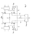
- the arrangement of the four field effect transistors S1 to S4 of the full bridge shown in FIG. 1 is identical to the known arrangement from FIG. 6. Again, a DC voltage U BUS is applied to the input of the full bridge circuit, the output of the full bridge circuit is formed by a shunt connected to ground. Resistor R. However, only the gas discharge lamp LA is now connected as a load; the elements of a resonance circuit are no longer present in the first exemplary embodiment. Switching between the two diagonals of the bridge again takes place through the two driver circuits T1 and T2, which control the four field effect transistors S1 to S4 in a suitable manner.
- the lamp brightness is no longer regulated by switching the switches S1 to S4 on and off by the driver circuits T1 and T2, but by controlling the field effect transistors S2 and S4 arranged in the bridge diagonals as controllable constant current sources.
- these two field effect transistors S2, S4 are each operated by an operational amplifier OP1 or OP2 in their modulation range. They thus form a resistor which is connected in series with the lamp LA and in this way defines an operating point for the lamp LA.
- the controllable constant current sources are thus formed by the two lower field effect transistors S2 and S4 of the two half bridges and the two operational amplifiers OP1 and OP2, each of which controls the corresponding field effect transistors S2 and S4.
- Via a feedback line 9 1 or 9 2 the current flowing through the respective field effect transistor S2 or S4 is supplied to the operational amplifier OP1, OP2 as an actual value, the second input signal forms a desired value I SET , corresponding to the desired lamp brightness, which, for example, the two operational amplifiers OP1, OP2 can be supplied by a dimming circuit or the like.
- the two operational amplifiers OP1 and OP2 act as controllers which set the current flowing through the two field effect transistors S2 and S4 to a value corresponding to the setpoint I SHOULD .
- the two driver circuits T1 and T2 are used to switch between the both bridge diagonals required control commands in the usual way by a Control circuit (not shown) supplied.
- a Control circuit (not shown) supplied.
- the two adjustable constant current sources can be used on a current limiting Inductance can be dispensed with.
- the voltage drop across them should be relatively low.
- the ballast also has a control circuit 1, to which the voltage dropping via the field effect transistor S2 or S4 of the respectively active bridge diagonal is supplied as an actual value via the two input lines 10 1 or 10 2 .
- This actual value is compared with a setpoint I FETsoll , which corresponds to the value that enables a particularly effective current control.
- the control circuit 1 generates a control signal which is used to control the DC voltage U BUS .
- Fig. 2 shows the block diagram of a ballast.
- the input of the ballast is formed by a rectifier circuit 11 connected to an AC voltage source, for example a full-bridge rectifier, which supplies a rectified AC voltage U 0 to a first switching regulator 3.
- This first switching regulator 3 is formed by a step-up converter, which generates a high intermediate circuit voltage U Z , which is fed to a second switching regulator 4.
- This second switching regulator 4 is a step-down converter which reduces the high intermediate circuit voltage U Z to the required lower value for the DC voltage U BUS .
- Reference number 2 denotes the full-bridge circuit shown in FIG. 1.
- the control circuit 1 controls the buck converter 4, in such a way that it generates a DC voltage U BUS , which, as provided, is only slightly above the lamp voltage LA, so that the via the two transistors S2 or S4 falling voltage corresponds to the setpoint U FETsoll .
- the control circuit 1 controls the buck converter 4, in such a way that it generates a DC voltage U BUS , which, as provided, is only slightly above the lamp voltage LA, so that the via the two transistors S2 or S4 falling voltage corresponds to the setpoint U FETsoll .
- U BUS DC voltage
- the control circuit 1 controls the buck converter 4, in such a way that it generates a DC voltage U BUS , which, as provided, is only slightly above the lamp voltage LA, so that the via the two transistors S2 or S4 falling voltage corresponds to the setpoint U FETsoll .
- U BUS DC voltage
- the control circuit 1 controls the buck converter 4, in such a way that it generates a DC voltage U
- the smoothing circuit for generating the DC voltage U BUS is not generated by two switching regulators connected in series, but by a buck boost converter 5, in which the functions of the switching regulators 3 and 4 shown in FIG. 2 are combined in one circuit.
- This integration is possible because the requirements for the control speed of the smoothing circuit are relatively low and there is therefore no fear of harmonics occurring at the input of the ballast due to rapid changes in frequency and / or duty cycle.
- the regulation of the lamp current by the two controllable Constant current sources has in addition to the suppression of flickering Consequence that when switching on the lamp LA at low lamp brightness no Lightning can occur because of the current due to the two adjustable constant current sources is limited to the desired value from the start. Ignition thus takes place the lamp LA at a current that has the lowest possible value for the Has triggered the ignition process.
- the buck converter 4 or the buck boost converter controlled that it has a maximum output voltage, which is used for the ignition is sufficient.
- Another option is to use a Ignition coil.
- the lamp wiring has no influence on the dimming operation Has. This is because switching continues at a low frequency, however, the high-frequency switching of switches is dispensed with and thus this "quasi-direct current" there is no influence of the wiring impedances.
- the low frequency pole reversal frequency i.e. the change between the two Bridge diagonals should be at least slightly above the frequency from Eye is still perceived, i.e. at least above 100 Hz. Especially a frequency between 700 Hz and 2000 Hz is advantageously selected.
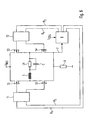
- FIG. 4 An embodiment of the full bridge circuit according to the invention is shown in FIG. 4. This differs on the one hand in that the gas discharge lamp LA is in turn part of a resonance circuit consisting of an inductor L and a capacitor C, which is connected as a load of the full-bridge circuit, and on the other hand in that the regulator 1 described in FIG. 1 to regulate the DC voltage U BUS is dispensed with.
- the full-bridge circuit 2 is supplied with a constant DC voltage U BUS , as is shown schematically in FIG. 5.
- the electronic ballast shown in FIG. 5 now has the rectifier circuit, a step-up converter 3 and the full-bridge circuit 2.
- the two controllable constant current sources consisting of the operational amplifiers OP1 and OP2 and the associated field-effect transistors S2 and S4 are provided in the full-bridge circuit shown in FIG. 4. Due to the constant DC voltage U BUS in its level, there is now the risk that at high lamp currents, that is to say at high brightness, the power loss resulting from the two transistors S2 and S4 will rise to an impermissible level.
- the function of the two controllable constant current sources is suppressed and the four transistors S1 to S4 are activated as in the known method shown in FIG. That is, a relatively low frequency is used to switch between the two diagonals of the bridge, one of the two transistors being clocked at high frequency during the on-time of a diagonal of the bridge, so that the lamp is operated with a direct current with a high-frequency ripple current superimposed on it.
- control with a variable pulse duty factor is necessary; in this operating mode, the inductance L forms the current-limiting impedance in series with the lamp.
- the control circuit 6 is again responsible for controlling the lamp brightness and transmits the corresponding control commands to the driver circuits T1 and T2 via lines 8 1 to 8 4 , which accordingly control the four transistors S1 to S4.
- the concept according to the invention is thus characterized in that lamp operation is realized with which dimming over a very wide brightness range is made possible.
- lamp operation is realized with which dimming over a very wide brightness range is made possible.
Landscapes
- Circuit Arrangements For Discharge Lamps (AREA)
- Inverter Devices (AREA)
Applications Claiming Priority (3)
| Application Number | Priority Date | Filing Date | Title |
|---|---|---|---|
| DE10051139A DE10051139A1 (de) | 2000-10-16 | 2000-10-16 | Elektronisches Vorschaltgerät mit Vollbrückenschaltung |
| DE10051139 | 2000-10-16 | ||
| EP01974243A EP1330945B1 (fr) | 2000-10-16 | 2001-09-11 | Ballast electronique avec circuit en pont integral |
Related Parent Applications (1)
| Application Number | Title | Priority Date | Filing Date |
|---|---|---|---|
| EP01974243A Division EP1330945B1 (fr) | 2000-10-16 | 2001-09-11 | Ballast electronique avec circuit en pont integral |
Publications (3)
| Publication Number | Publication Date |
|---|---|
| EP1465465A2 true EP1465465A2 (fr) | 2004-10-06 |
| EP1465465A3 EP1465465A3 (fr) | 2004-10-13 |
| EP1465465B1 EP1465465B1 (fr) | 2008-12-31 |
Family
ID=7659903
Family Applications (2)
| Application Number | Title | Priority Date | Filing Date |
|---|---|---|---|
| EP01974243A Expired - Lifetime EP1330945B1 (fr) | 2000-10-16 | 2001-09-11 | Ballast electronique avec circuit en pont integral |
| EP04013891A Expired - Lifetime EP1465465B1 (fr) | 2000-10-16 | 2001-09-11 | Ballast électronique avec un circuit en pont complet |
Family Applications Before (1)
| Application Number | Title | Priority Date | Filing Date |
|---|---|---|---|
| EP01974243A Expired - Lifetime EP1330945B1 (fr) | 2000-10-16 | 2001-09-11 | Ballast electronique avec circuit en pont integral |
Country Status (8)
| Country | Link |
|---|---|
| US (1) | US6876158B2 (fr) |
| EP (2) | EP1330945B1 (fr) |
| AT (2) | ATE291341T1 (fr) |
| AU (2) | AU2001293807B2 (fr) |
| BR (1) | BR0114678A (fr) |
| DE (3) | DE10051139A1 (fr) |
| WO (1) | WO2002034015A1 (fr) |
| ZA (1) | ZA200302354B (fr) |
Cited By (1)
| Publication number | Priority date | Publication date | Assignee | Title |
|---|---|---|---|---|
| EP2223572A1 (fr) * | 2007-12-14 | 2010-09-01 | Koninklijke Philips Electronics N.V. | Générateur de lumière atténuable |
Families Citing this family (13)
| Publication number | Priority date | Publication date | Assignee | Title |
|---|---|---|---|---|
| EP1579743A1 (fr) * | 2002-12-20 | 2005-09-28 | Koninklijke Philips Electronics N.V. | Mise sous tension a deux etats de lampes hid |
| DE102004016945A1 (de) * | 2004-04-06 | 2005-10-27 | Patent-Treuhand-Gesellschaft für elektrische Glühlampen mbH | EVG mit Regelschaltung und Störgrößenaufschaltung |
| KR100695525B1 (ko) * | 2005-01-31 | 2007-03-15 | 주식회사 하이닉스반도체 | 반도체 기억 소자의 지연 고정 루프 |
| EP1689212B1 (fr) * | 2005-02-02 | 2008-01-23 | Patent-Treuhand-Gesellschaft für elektrische Glühlampen mbH | Méthode et dispositif pour varier l' intensité lumineuse de sources de lumière |
| DE102005028672A1 (de) * | 2005-06-21 | 2006-12-28 | Patent-Treuhand-Gesellschaft für elektrische Glühlampen mbH | Glättungsschaltung zur Verbesserung der EMV |
| DE102006018569A1 (de) * | 2006-04-21 | 2007-10-25 | Tridonicatco Gmbh & Co. Kg | Dimmbares elektronisches Vorschaltgerät |
| US8076871B2 (en) * | 2007-04-27 | 2011-12-13 | Koninklijke Philips Electronics N.V. | Driver apparatus for a gas discharge lamp |
| GB2449931B (en) * | 2007-06-08 | 2011-11-16 | E2V Tech | Power supply for radio frequency heating apparatus |
| DE102007049397A1 (de) | 2007-10-15 | 2009-04-16 | Tridonicatco Gmbh & Co. Kg | DC-Versorgung, insbesondere für Leuchtdioden, in einem Betriebsgerät mit Wechselrichter |
| CN101884252B (zh) * | 2007-12-03 | 2013-05-01 | 皇家飞利浦电子股份有限公司 | 驱动气体放电灯的方法 |
| KR20110079905A (ko) | 2008-10-23 | 2011-07-11 | 오스람 게젤샤프트 미트 베쉬랭크터 하프퉁 | 고압 방전 램프를 동작시키기 위한 회로 어레인지먼트 및 방법 |
| US9513402B2 (en) | 2011-08-23 | 2016-12-06 | Exxonmobil Upstream Research Company | Estimating fracture dimensions from microseismic data |
| US8754583B2 (en) * | 2012-01-19 | 2014-06-17 | Technical Consumer Products, Inc. | Multi-level adaptive control circuitry for deep phase-cut dimming compact fluorescent lamp |
Family Cites Families (17)
| Publication number | Priority date | Publication date | Assignee | Title |
|---|---|---|---|---|
| US4346332A (en) * | 1980-08-14 | 1982-08-24 | General Electric Company | Frequency shift inverter for variable power control |
| JPS61159702A (ja) * | 1984-12-29 | 1986-07-19 | 株式会社村田製作所 | 有機正特性サ−ミスタ |
| AT392384B (de) | 1985-02-04 | 1991-03-25 | Zumtobel Ag | Vorschaltgeraet zum betrieb von gasentladungslampen mit gleichstrom |
| JPH04109952A (ja) | 1990-08-31 | 1992-04-10 | Toshiba Lighting & Technol Corp | 紫外線照射装置 |
| US5491388A (en) * | 1992-03-25 | 1996-02-13 | Toto Ltd. | Power regulator of discharge lamp and variable color illumination apparatus using the regulator |
| DE4238388C2 (de) * | 1992-11-13 | 1997-02-20 | Heidelberger Druckmasch Ag | Elektronische Schaltungsanordnung zur Ansteuerung einer UV-Strahlungsquelle |
| DE4416042A1 (de) * | 1993-06-25 | 1995-01-05 | Prolux Maschinenbau Gmbh | Schaltungsanordnung zum Betrieb von Entladungslampen |
| DE4401630A1 (de) | 1994-01-20 | 1995-07-27 | Bischl Johann | Zünd- und Betriebsgerät für den Gleichstrombetrieb von Gasentladungslampen |
| FR2721475B1 (fr) * | 1994-06-15 | 1996-07-19 | Sgs Thomson Microelectronics | Circuit de commande de commutation et dispositif de commande pour lampe fluorescente à basse pression. |
| DE19523750A1 (de) * | 1995-06-29 | 1997-01-02 | Thomson Brandt Gmbh | Wechselstromquelle |
| US6124682A (en) * | 1996-11-19 | 2000-09-26 | Micro Tech Limited | Lamp driver circuit using resonant circuit for starting lamp |
| US5932976A (en) * | 1997-01-14 | 1999-08-03 | Matsushita Electric Works R&D Laboratory, Inc. | Discharge lamp driving |
| US5817413A (en) * | 1997-05-20 | 1998-10-06 | Nyacol Products, Inc. | High shear pipeline tape |
| JP3488807B2 (ja) * | 1997-05-26 | 2004-01-19 | セイコープレシジョン株式会社 | El素子の駆動回路 |
| GB9714785D0 (en) * | 1997-07-14 | 1997-09-17 | Sheffield University | Discharge lamp |
| JP3829507B2 (ja) * | 1997-12-12 | 2006-10-04 | 松下電工株式会社 | 電子バラストおよびhidランプ制御回路 |
| AU747501B2 (en) * | 1998-09-18 | 2002-05-16 | Knobel Ag Lichttechnische Komponenten | Circuit for operating gas discharge lamps |
-
2000
- 2000-10-16 DE DE10051139A patent/DE10051139A1/de not_active Ceased
-
2001
- 2001-09-11 AU AU2001293807A patent/AU2001293807B2/en not_active Ceased
- 2001-09-11 EP EP01974243A patent/EP1330945B1/fr not_active Expired - Lifetime
- 2001-09-11 AU AU9380701A patent/AU9380701A/xx active Pending
- 2001-09-11 ZA ZA200302354A patent/ZA200302354B/en unknown
- 2001-09-11 WO PCT/EP2001/010497 patent/WO2002034015A1/fr not_active Ceased
- 2001-09-11 BR BR0114678-5A patent/BR0114678A/pt not_active Application Discontinuation
- 2001-09-11 EP EP04013891A patent/EP1465465B1/fr not_active Expired - Lifetime
- 2001-09-11 DE DE50105645T patent/DE50105645D1/de not_active Expired - Lifetime
- 2001-09-11 DE DE50114634T patent/DE50114634D1/de not_active Expired - Lifetime
- 2001-09-11 AT AT01974243T patent/ATE291341T1/de not_active IP Right Cessation
- 2001-09-11 AT AT04013891T patent/ATE419735T1/de not_active IP Right Cessation
-
2003
- 2003-04-16 US US10/414,319 patent/US6876158B2/en not_active Expired - Fee Related
Cited By (2)
| Publication number | Priority date | Publication date | Assignee | Title |
|---|---|---|---|---|
| EP2223572A1 (fr) * | 2007-12-14 | 2010-09-01 | Koninklijke Philips Electronics N.V. | Générateur de lumière atténuable |
| RU2482639C2 (ru) * | 2007-12-14 | 2013-05-20 | Конинклейке Филипс Электроникс Н.В. | Регулируемое светогенерирующее устройство |
Also Published As
| Publication number | Publication date |
|---|---|
| EP1330945A1 (fr) | 2003-07-30 |
| US6876158B2 (en) | 2005-04-05 |
| AU2001293807B2 (en) | 2006-02-16 |
| ZA200302354B (en) | 2004-03-26 |
| BR0114678A (pt) | 2003-10-07 |
| DE50105645D1 (de) | 2005-04-21 |
| EP1465465A3 (fr) | 2004-10-13 |
| DE10051139A1 (de) | 2002-04-25 |
| DE50114634D1 (de) | 2009-02-12 |
| US20040004447A1 (en) | 2004-01-08 |
| EP1330945B1 (fr) | 2005-03-16 |
| EP1465465B1 (fr) | 2008-12-31 |
| AU9380701A (en) | 2002-04-29 |
| ATE419735T1 (de) | 2009-01-15 |
| WO2002034015A1 (fr) | 2002-04-25 |
| ATE291341T1 (de) | 2005-04-15 |
Similar Documents
| Publication | Publication Date | Title |
|---|---|---|
| DE69704082T2 (de) | Steuerschaltung und -verfahren für piezoelektrischen transformator | |
| DE69919138T2 (de) | Electronischer dimmer | |
| DE69816023T2 (de) | Schaltungsanordnung | |
| DE4332059B4 (de) | Vorschaltgerät zur Helligkeitssteuerung von Entladungslampen | |
| EP1330945B1 (fr) | Ballast electronique avec circuit en pont integral | |
| DE3829388A1 (de) | Schaltungsanordnung zum betrieb einer last | |
| DE102005006587B4 (de) | Wechselrichter insbesondere für eine konstante Lichtabgabe einer Kaltkathodenfluoreszenzlampe und Verfahren zum Betrieb dieses Wechselrichters | |
| DE69315761T2 (de) | Geschützter Umrichter zur Steuerung einer Entladungslampe | |
| EP1465330A2 (fr) | Procédé pour varier la consommation de puissance de charges capacitives | |
| EP1467474B1 (fr) | Circuit d'interface pour opérer des charges capacitives | |
| DE60318326T2 (de) | Schaltungsanordnung zum betrieb von gasentladungslampen | |
| EP2952060B1 (fr) | Circuit électrique et procédé pour faire fonctionner et varier au moins une led | |
| DE69308986T2 (de) | Schaltung und Verfahren zum Betreiben von Starkentladungslampen durch Rückwirkung | |
| DE102017221786A1 (de) | Lampenbetriebsgerät mit Konverter im DCM | |
| EP2266374B1 (fr) | Régulation de puissance de lampes à décharge dans des circuits en demi-pont ou en pont intégral | |
| EP1189490B1 (fr) | Ballast électronique de lampe fluorescente | |
| DE29622825U1 (de) | Bestrahlungsgerät | |
| EP1589645A2 (fr) | Circuit pour convertir une tension alternative en tension continue | |
| EP1696713B1 (fr) | Ballast électronique avec dispositif de mesure de courant pour lampe à décharge haute-pression | |
| DE102005025682B4 (de) | Vorrichtung zur Ansteuerung von Leuchtstofflampen in einer Beleuchtungsanordnung | |
| DE4233861A1 (de) | Einrichtung zur Ansteuerung von Hochspannungsentladungslampen sowie ein Verfahren hierfür | |
| WO2018172054A1 (fr) | Procédé et convertisseur cadencé pour le fonctionnement de sources de lumière formant rapidement une puissance d'entrée | |
| WO2012010591A2 (fr) | Convertisseur abaisseur de tension pour fournir un courant pour au moins une del | |
| EP0922376A1 (fr) | Allast electronique pour lampes a decharge | |
| EP1198159A1 (fr) | Ballast électronique |
Legal Events
| Date | Code | Title | Description |
|---|---|---|---|
| PUAI | Public reference made under article 153(3) epc to a published international application that has entered the european phase |
Free format text: ORIGINAL CODE: 0009012 |
|
| PUAL | Search report despatched |
Free format text: ORIGINAL CODE: 0009013 |
|
| 17P | Request for examination filed |
Effective date: 20040614 |
|
| AC | Divisional application: reference to earlier application |
Ref document number: 1330945 Country of ref document: EP Kind code of ref document: P |
|
| AK | Designated contracting states |
Kind code of ref document: A2 Designated state(s): AT BE CH CY DE DK ES FI FR GB GR IE IT LI LU MC NL PT SE TR |
|
| AK | Designated contracting states |
Kind code of ref document: A3 Designated state(s): AT BE CH CY DE DK ES FI FR GB GR IE IT LI LU MC NL PT SE TR |
|
| AKX | Designation fees paid |
Designated state(s): AT BE CH CY DE DK ES FI FR GB GR IE IT LI LU MC NL PT SE TR |
|
| 17Q | First examination report despatched |
Effective date: 20051114 |
|
| GRAP | Despatch of communication of intention to grant a patent |
Free format text: ORIGINAL CODE: EPIDOSNIGR1 |
|
| GRAS | Grant fee paid |
Free format text: ORIGINAL CODE: EPIDOSNIGR3 |
|
| GRAA | (expected) grant |
Free format text: ORIGINAL CODE: 0009210 |
|
| AC | Divisional application: reference to earlier application |
Ref document number: 1330945 Country of ref document: EP Kind code of ref document: P |
|
| AK | Designated contracting states |
Kind code of ref document: B1 Designated state(s): AT BE CH CY DE DK ES FI FR GB GR IE IT LI LU MC NL PT SE TR |
|
| REG | Reference to a national code |
Ref country code: CH Ref legal event code: EP Ref country code: GB Ref legal event code: FG4D Free format text: NOT ENGLISH |
|
| REF | Corresponds to: |
Ref document number: 50114634 Country of ref document: DE Date of ref document: 20090212 Kind code of ref document: P |
|
| REG | Reference to a national code |
Ref country code: IE Ref legal event code: FG4D Free format text: LANGUAGE OF EP DOCUMENT: GERMAN |
|
| PG25 | Lapsed in a contracting state [announced via postgrant information from national office to epo] |
Ref country code: FI Free format text: LAPSE BECAUSE OF FAILURE TO SUBMIT A TRANSLATION OF THE DESCRIPTION OR TO PAY THE FEE WITHIN THE PRESCRIBED TIME-LIMIT Effective date: 20081231 Ref country code: NL Free format text: LAPSE BECAUSE OF FAILURE TO SUBMIT A TRANSLATION OF THE DESCRIPTION OR TO PAY THE FEE WITHIN THE PRESCRIBED TIME-LIMIT Effective date: 20081231 |
|
| NLV1 | Nl: lapsed or annulled due to failure to fulfill the requirements of art. 29p and 29m of the patents act | ||
| PG25 | Lapsed in a contracting state [announced via postgrant information from national office to epo] |
Ref country code: ES Free format text: LAPSE BECAUSE OF FAILURE TO SUBMIT A TRANSLATION OF THE DESCRIPTION OR TO PAY THE FEE WITHIN THE PRESCRIBED TIME-LIMIT Effective date: 20090411 |
|
| REG | Reference to a national code |
Ref country code: IE Ref legal event code: FD4D |
|
| PG25 | Lapsed in a contracting state [announced via postgrant information from national office to epo] |
Ref country code: PT Free format text: LAPSE BECAUSE OF FAILURE TO SUBMIT A TRANSLATION OF THE DESCRIPTION OR TO PAY THE FEE WITHIN THE PRESCRIBED TIME-LIMIT Effective date: 20090601 Ref country code: SE Free format text: LAPSE BECAUSE OF FAILURE TO SUBMIT A TRANSLATION OF THE DESCRIPTION OR TO PAY THE FEE WITHIN THE PRESCRIBED TIME-LIMIT Effective date: 20090331 |
|
| PG25 | Lapsed in a contracting state [announced via postgrant information from national office to epo] |
Ref country code: DK Free format text: LAPSE BECAUSE OF FAILURE TO SUBMIT A TRANSLATION OF THE DESCRIPTION OR TO PAY THE FEE WITHIN THE PRESCRIBED TIME-LIMIT Effective date: 20081231 Ref country code: IE Free format text: LAPSE BECAUSE OF FAILURE TO SUBMIT A TRANSLATION OF THE DESCRIPTION OR TO PAY THE FEE WITHIN THE PRESCRIBED TIME-LIMIT Effective date: 20081231 |
|
| PLBE | No opposition filed within time limit |
Free format text: ORIGINAL CODE: 0009261 |
|
| STAA | Information on the status of an ep patent application or granted ep patent |
Free format text: STATUS: NO OPPOSITION FILED WITHIN TIME LIMIT |
|
| 26N | No opposition filed |
Effective date: 20091001 |
|
| BERE | Be: lapsed |
Owner name: TRIDONICATCO GMBH & CO. KG Effective date: 20090930 |
|
| PG25 | Lapsed in a contracting state [announced via postgrant information from national office to epo] |
Ref country code: MC Free format text: LAPSE BECAUSE OF NON-PAYMENT OF DUE FEES Effective date: 20090930 |
|
| REG | Reference to a national code |
Ref country code: CH Ref legal event code: PL |
|
| PG25 | Lapsed in a contracting state [announced via postgrant information from national office to epo] |
Ref country code: BE Free format text: LAPSE BECAUSE OF NON-PAYMENT OF DUE FEES Effective date: 20090930 |
|
| PG25 | Lapsed in a contracting state [announced via postgrant information from national office to epo] |
Ref country code: GR Free format text: LAPSE BECAUSE OF FAILURE TO SUBMIT A TRANSLATION OF THE DESCRIPTION OR TO PAY THE FEE WITHIN THE PRESCRIBED TIME-LIMIT Effective date: 20090401 Ref country code: CH Free format text: LAPSE BECAUSE OF NON-PAYMENT OF DUE FEES Effective date: 20090930 Ref country code: LI Free format text: LAPSE BECAUSE OF NON-PAYMENT OF DUE FEES Effective date: 20090930 |
|
| PG25 | Lapsed in a contracting state [announced via postgrant information from national office to epo] |
Ref country code: AT Free format text: LAPSE BECAUSE OF NON-PAYMENT OF DUE FEES Effective date: 20090911 |
|
| PG25 | Lapsed in a contracting state [announced via postgrant information from national office to epo] |
Ref country code: IT Free format text: LAPSE BECAUSE OF FAILURE TO SUBMIT A TRANSLATION OF THE DESCRIPTION OR TO PAY THE FEE WITHIN THE PRESCRIBED TIME-LIMIT Effective date: 20081231 |
|
| PG25 | Lapsed in a contracting state [announced via postgrant information from national office to epo] |
Ref country code: LU Free format text: LAPSE BECAUSE OF NON-PAYMENT OF DUE FEES Effective date: 20090911 |
|
| PG25 | Lapsed in a contracting state [announced via postgrant information from national office to epo] |
Ref country code: TR Free format text: LAPSE BECAUSE OF FAILURE TO SUBMIT A TRANSLATION OF THE DESCRIPTION OR TO PAY THE FEE WITHIN THE PRESCRIBED TIME-LIMIT Effective date: 20081231 |
|
| PG25 | Lapsed in a contracting state [announced via postgrant information from national office to epo] |
Ref country code: CY Free format text: LAPSE BECAUSE OF FAILURE TO SUBMIT A TRANSLATION OF THE DESCRIPTION OR TO PAY THE FEE WITHIN THE PRESCRIBED TIME-LIMIT Effective date: 20081231 |
|
| PGFP | Annual fee paid to national office [announced via postgrant information from national office to epo] |
Ref country code: FR Payment date: 20111012 Year of fee payment: 11 |
|
| PGFP | Annual fee paid to national office [announced via postgrant information from national office to epo] |
Ref country code: DE Payment date: 20121130 Year of fee payment: 12 |
|
| REG | Reference to a national code |
Ref country code: FR Ref legal event code: ST Effective date: 20130531 |
|
| PG25 | Lapsed in a contracting state [announced via postgrant information from national office to epo] |
Ref country code: FR Free format text: LAPSE BECAUSE OF NON-PAYMENT OF DUE FEES Effective date: 20121001 |
|
| REG | Reference to a national code |
Ref country code: DE Ref legal event code: R119 Ref document number: 50114634 Country of ref document: DE Effective date: 20140401 |
|
| PG25 | Lapsed in a contracting state [announced via postgrant information from national office to epo] |
Ref country code: DE Free format text: LAPSE BECAUSE OF NON-PAYMENT OF DUE FEES Effective date: 20140401 |
|
| PGFP | Annual fee paid to national office [announced via postgrant information from national office to epo] |
Ref country code: GB Payment date: 20140929 Year of fee payment: 14 |
|
| GBPC | Gb: european patent ceased through non-payment of renewal fee |
Effective date: 20150911 |
|
| PG25 | Lapsed in a contracting state [announced via postgrant information from national office to epo] |
Ref country code: GB Free format text: LAPSE BECAUSE OF NON-PAYMENT OF DUE FEES Effective date: 20150911 |