EP1467216A2 - Verfahren zur Herstellung eines Magnetfelddetektors - Google Patents
Verfahren zur Herstellung eines Magnetfelddetektors Download PDFInfo
- Publication number
- EP1467216A2 EP1467216A2 EP04251015A EP04251015A EP1467216A2 EP 1467216 A2 EP1467216 A2 EP 1467216A2 EP 04251015 A EP04251015 A EP 04251015A EP 04251015 A EP04251015 A EP 04251015A EP 1467216 A2 EP1467216 A2 EP 1467216A2
- Authority
- EP
- European Patent Office
- Prior art keywords
- coil
- forming
- soft magnetic
- semiconductor substrate
- magnetic core
- Prior art date
- Legal status (The legal status is an assumption and is not a legal conclusion. Google has not performed a legal analysis and makes no representation as to the accuracy of the status listed.)
- Granted
Links
Images




Classifications
-
- G—PHYSICS
- G01—MEASURING; TESTING
- G01R—MEASURING ELECTRIC VARIABLES; MEASURING MAGNETIC VARIABLES
- G01R33/00—Arrangements or instruments for measuring magnetic variables
- G01R33/02—Measuring direction or magnitude of magnetic fields or magnetic flux
-
- G—PHYSICS
- G01—MEASURING; TESTING
- G01R—MEASURING ELECTRIC VARIABLES; MEASURING MAGNETIC VARIABLES
- G01R33/00—Arrangements or instruments for measuring magnetic variables
- G01R33/02—Measuring direction or magnitude of magnetic fields or magnetic flux
- G01R33/04—Measuring direction or magnitude of magnetic fields or magnetic flux using the flux-gate principle
-
- G—PHYSICS
- G01—MEASURING; TESTING
- G01R—MEASURING ELECTRIC VARIABLES; MEASURING MAGNETIC VARIABLES
- G01R33/00—Arrangements or instruments for measuring magnetic variables
- G01R33/02—Measuring direction or magnitude of magnetic fields or magnetic flux
- G01R33/04—Measuring direction or magnitude of magnetic fields or magnetic flux using the flux-gate principle
- G01R33/05—Measuring direction or magnitude of magnetic fields or magnetic flux using the flux-gate principle in thin-film element
-
- H—ELECTRICITY
- H01—ELECTRIC ELEMENTS
- H01F—MAGNETS; INDUCTANCES; TRANSFORMERS; SELECTION OF MATERIALS FOR THEIR MAGNETIC PROPERTIES
- H01F41/00—Apparatus or processes specially adapted for manufacturing or assembling magnets, inductances or transformers; Apparatus or processes specially adapted for manufacturing materials characterised by their magnetic properties
- H01F41/02—Apparatus or processes specially adapted for manufacturing or assembling magnets, inductances or transformers; Apparatus or processes specially adapted for manufacturing materials characterised by their magnetic properties for manufacturing cores, coils, or magnets
- H01F41/04—Apparatus or processes specially adapted for manufacturing or assembling magnets, inductances or transformers; Apparatus or processes specially adapted for manufacturing materials characterised by their magnetic properties for manufacturing cores, coils, or magnets for manufacturing coils
- H01F41/041—Printed circuit coils
- H01F41/046—Printed circuit coils structurally combined with ferromagnetic material
-
- H—ELECTRICITY
- H01—ELECTRIC ELEMENTS
- H01F—MAGNETS; INDUCTANCES; TRANSFORMERS; SELECTION OF MATERIALS FOR THEIR MAGNETIC PROPERTIES
- H01F17/00—Fixed inductances of the signal type
- H01F17/0006—Printed inductances
Definitions
- the present invention relates to a method for manufacturing a magnetic field detecting device by forming a soft magnetic core and a coil in a thin film type on a semiconductor substrate using a semiconductor process.
- a magnetic sensor using a soft magnetic material and a coil has been used as a magnetic sensor of high sensitivity for a long time.
- Such magnetic sensor is usually manufactured by a coil wound on a soft magnetic core, and requires an electronic circuit for obtaining magnetic field proportional to measured magnetic field.
- Recently, a method for realizing such magnetic filed detecting element of the magnetic sensor in form of the soft magnetic thin film core and a plane thin film coil on the semiconductor substrate using the semiconductor process, has been suggested.
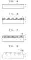
- FIG. 1A through FIG. 1J A general method for manufacturing a magnetic field detecting element using the semiconductor process will be briefly described with reference to FIG. 1A through FIG. 1J in the following.
- the first seed film 2 is formed on a semiconductor substrate 1.
- the first plating mold 3 having a plurality of grooves 3a is formed by exposing and developing processes as shown in FIG. 1B.
- metal is filled up in the groove 3a of the first plating mold 3 through the process such as an electric plating so that a plurality of coil lines 4a, 4b,... may be formed as shown in FIG. 1C.
- the first plating mold 3 and the seed film under the plating mold 3 are removed so that the first coil 4 consisting of a plurality of coil lines 4a, 4b,...that are insulated each other may be formed as shown in FIG. 1D.
- the first insulating film 5 is formed at the height higher than the height of the first coil 4 on the semiconductor substrate 1 as shown in FIG. 1E. After that, a soft magnetic material film is spread on the upper part of the first insulating film 5 and a soft magnetic core 6 is formed by a pattern formation and etching (refer to FIG. 1F).
- a second insulating film 7 of a predetermined thickness is formed on the soft magnetic core 6 of the semiconductor substrate 1 as shown in FIG. 1G, and as shown in FIG. 1H, via holes 8a, 8b for communicating with the coil lines 4a, 4o forming both ends of the first coil 4, are formed, and a second seed film 9 is formed in a predetermined thickness on the upper part of the second insulating film 7, then a photoresist is spread thick on the second seed film 9 and the second plating mold 10 having a plurality of grooves 10a is formed by exposing and developing processes.
- metal is filled up in the groove 10a of the second plating mold 10 so that a plurality of coil lines 11a, 11b,...may be formed.
- the second plating mold 10 and the second seed film 9 under the second plating mold 10 are removed so that the second coil 11 consisting of a plurality of coil lines 11a, 11b,...that are insulated each other may be formed as shown in FIG. 1J.
- a protection film is spread on the upper part of the second coil 11, whereby manufacturing of the magnetic field detecting element is completed.
- the seed film 2 between the coil lines 4a, 4b,... should be removed in order for each coil line 4a, 4b,...constituting the first coil 4 to be insulated from each other.
- the process of spreading the insulating film 5 again is added for the subsequent process, whereby the manufacturing process is complicated.
- the performance of the soft magnetic core 6 in the foregoing magnetic field detecting element is not very good in case that the semiconductor substrate 1 for supporting the core is not even.
- the general magnetic field detecting element Since having a structure in which the first coil 4 projects from the semiconductor substrate 1, the general magnetic field detecting element has weak point that the thickness of the first and the second insulating films 5, 7 for insulation and planarization, becomes thick. If the thickness of the insulating films 5, 7 becomes thick, not only the whole thickness of the element becomes thick but also the process for forming the via holes 8a, 8b for connecting the first coil 4 with the second coil 11 becomes difficult. Also, a pitch between the coil lines that has an influence on the performance of the sensor gets large, which shows a negative effect.
- a method for manufacturing a magnetic field detecting element consisting of a soft magnetic core formed on a semiconductor substrate; a first and a second coils arranged on the upper and the lower parts of the soft magnetic core, and having a plurality of coil lines, respectively, the method comprising the steps of: forming a seed film of a predetermined thickness on the semiconductor substrate; removing the seed film in a predetermined pattern so that a plurality of the coil lines constituting the first coil that would be formed on the seed film may be partitioned each other; forming a first plating mold having a plurality of grooves that corresponds to the predetermined pattern, on an upper part of the seed film; forming a plurality of the coil lines constituting the first coil by filling up metal in the groove of the first plating mold; forming a soft magnetic core and the second coil on an upper part of the semiconductor substrate where the first coil is formed; and cutting off four edges of the semiconductor substrate so that a plurality of the coil lines partitioned by the predetermined pattern
- the step of removing the seed film further comprises the steps of: spreading a photoresist on an upper surface of the seed film; forming a predetermined pattern that would be removed, by exposing and developing the photoresist: and etching the seed film according to the pattern.
- metal is filled up in the groove of the first plating mold with use of an electric plating.
- the step of forming a soft magnetic core further comprises the steps of: performing planarization of an upper surface of the semiconductor substrate on which the first coil is formed; spreading an insulating film on an upper surface of the semiconductor substrate for which planarization has been performed; spreading a soft magnetic material film on an upper part of the insulating film; forming a pattern of a soft magnetic core through exposing and developing processes after spreading a photoresist on the soft magnetic material film; and etching the soft magnetic material film according to the pattern.
- the step of forming a soft magnetic core could also be realized by other method comprising the steps of: removing the first plating mold; spreading an insulating film at a height higher than a height of the first coil, on an upper part of the semiconductor substrate from which the first plating mold has been removed; spreading a soft magnetic material film on an upper part of the insulating film; forming a pattern of a soft magnetic core through exposing and developing processes after spreading a photoresist on the soft magnetic material film; and etching the soft magnetic material film according to the pattern.
- a magnetic field detecting element consisting of a soft magnetic core formed on a semiconductor substrate; a first and a second coils arranged on upper and lower parts of the soft magnetic core, and having a plurality of coil lines, respectively, the method comprising the steps of: forming a first seed film of a predetermined thickness on the semiconductor substrate; removing the first seed film in a predetermined first pattern so that a plurality of coil lines constituting the first coil that would be formed on the first seed film may be partitioned each other; forming a first plating mold having a plurality of grooves that correspond to the predetermined first pattern, on an upper part of the first seed film; forming a plurality of coil lines constituting the first coil by filling up metal in the groove of the first plating mold; forming a soft magnetic core on the semiconductor substrate where the first coil is formed; forming a second insulating film on the semiconductor substrate where the soft magnetic core
- a method for manufacturing a magnetic field detecting element including the steps of: forming a first coil on an upper part of a semiconductor substrate; after forming a soft magnetic core on an upper part of the first coil with an insulating film intervened, forming a second coil on an upper part of the soft magnetic core with another insulating film intervened, the method comprising the step of: after forming a well of a predetermined depth on the semiconductor substrate, arranging the first coil in an inside of the well lest the first coil should be projected to a surface of the semiconductor substrate.
- a method for manufacturing a magnetic field detecting element comprising the steps of: preparing a semiconductor substrate; forming a well of a predetermined depth on the semiconductor substrate; forming a first coil consisting of a plurality of coil lines in the inside of the well of the semiconductor substrate; forming a first insulating film on an upper part of the semiconductor substrate including the well; forming a soft magnetic core on an upper part of the first insulating film; forming a second insulating film on an upper part of the first insulating film including the soft magnetic core; and forming a second coil that corresponds to the first coil, on an upper part of the second insulating film.
- the well is formed in such a way that the well has an inclined sidewall that is gradually inclined in its inside from its upper part to its bottom by the etching process.
- the step of forming the first coil further comprises the steps of: forming a first seed film on a surface of the well; forming a first plating mold having a plurality of grooves on the first seed film; forming a plurality of coil lines constituting the first coil by filling up metal in each groove of the first plating mold; and removing the first plating mold and the first seed film under the first plating mold.
- the step of forming the second coil further comprises the steps of: forming a via hole by etching the first and the second insulating films on both sides of the soft magnetic core; forming a second seed film on an upper surface of the second insulating film on which the via hole is formed; forming a second plating mold having a plurality of grooves, on the second seed film; forming a plurality of coil lines constituting a second coil by filling up metal in each groove of the second plating mold, and connecting the first coil with the second coil through the via hole; and removing the second plating mold and the second seed film under the second plating mold.
- a method for manufacturing a magnetic field detecting element according to the present invention further comprises the step of forming a protection film for protecting structures including the second coil.
- a magnetic field detecting element comprising: a semiconductor substrate; a soft magnetic core formed on an upper part of the semiconductor substrate; an insulating film positioned on an upper and a lower parts of the soft magnetic core; and a first and a second coils formed in such a way that those coils enclose the soft magnetic core with the soft magnetic core and the insulating film intervened, and having a plurality of coil lines, respectively, wherein a well of a predetermined depth is formed on the semiconductor substrate and the coil lines constituting the first coil are arranged in the inside of the well.
- a magnetic field detecting element has the construction such that a height of the coil lines and a depth of the well are the same.
- the first coil is positioned at the lower part of the soft magnetic core and the second coil is positioned at the upper part of the soft magnetic core, and the coil lines of the first and the second coils are connected by means of a third coil filled in the via hole formed by passing through the insulating film on both sides of the soft magnetic core.
- the well has an inclined sidewall that is gradually inclined in its inside from its upper part to its bottom.
- the invention provides a method for manufacturing a magnetic field detecting element, wherein manufacturing process is simple and there are small restrictions in materials usable for an insulating film, since a plating mold does not need to be removed for removal of the seed film for insulation between coil lines.
- the method is capable of easily performing planarization of the semiconductor substrate on which a coil is formed, and simplifies the process since the thickness of the planarization material is thin.
- FIG 2A through FIG 2K are views showing process of a method for manufacturing a magnetic field detecting element according to an embodiment of the present invention.
- the first step in the method for manufacturing a magnetic field detecting element according to an embodiment of the present invention is to form an oxidation film (not shown) for electric insulation, on a semiconductor substrate 100, and to form the first seed layer 102 for plating, on that oxidation film as shown in FIG. 2A.
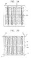
- the first seed film 102 spread on the semiconductor substrate 100 is partially removed with use of a predetermined pattern, i.e., the pattern as shown in FIG. 3A.
- the removal of the first seed film 102 is for insulating, in a simple manner, a plurality of coil lines constituting the first coil that would be formed on the first seed film 102 as will be described below.
- the reference numerals 103 and 107 in FIG. 3A are a seed film pattern to be removed and a position of a plurality of the coil lines.
- the pattern 103 is positioned between a plurality of the coil lines, whereby a plurality of the coil lines is partitioned from the neighboring coil lines and connected through the seed film at the edges.
- FIG. 3B if four lines 110 connecting the edges of the pattern 103 are cut, the positions of the coil lines are insulated each other.
- the removal of such first seed film 102 is performed in the following way, in which the seed film pattern 103 that would be removed by exposing and developing processes is formed after the photoresist is spread on the first seed film 102. At this time, the seed film pattern 103 that would be removed is formed in such a way that parts 102b where a plurality of coil lines 107 constituting the first coil 106 are to be formed, are insulated from each other and edges 102a are connected each other as shown in FIG. 3A.
- the seed film 102 is electrically connected from the viewpoint of the whole semiconductor substrate 100, but the parts 102b where a plurality of the coil lines 107 constituting the first coil 106 would be formed, is formed in such a way that the parts 102b could be electrically insulated each other if the connection parts, i.e., the edges 102a are cut.
- the first coil is formed in such a way that an exciting coil and an magnetic field detecting coil are wired one time by turns. Also, only one of either the exciting coil or the magnetic field detecting coil may be wired in form of a solenoid.
- the pattern 103 of the seed film 102 is removed through etching, then the photoresist is removed, whereby partial removal of the seed film is completed.
- the first plating mold 104 having a plurality of grooves 104a is formed by exposing and developing processes (refer to FIG. 2C), and metal is filled in the groove 104a of the first mold 104, so that a plurality of coil lines 107, 107a constituting the first coil 106, is formed.
- metal sticks to and grows on the seed film in the lower part of the groove 104a of the first plating mold 104, whereby a plurality of coil lines 107, 107a is formed as shown in FIG. 2D.
- a first insulating film 120 is formed in a predetermined thickness on that evenly processed upper surface as shown in FIG. 2E. Then, a soft magnetic material film is stacked on the upper part of the first insulating film 120 and a soft magnetic core 122 is formed by pattern formation and etching (refer to FIG. 2F).
- the insulating film for forming the soft magnetic core 122 may be formed in such a way that the first plating mold 104 is removed and the insulating material is spread in a height higher than a height of the first coil 106, on the semiconductor substrate 100 so that a first insulating film 120A is formed as shown in FIG. 4. According to such method, there is a strong point that planarization process needs not to be performed.
- a second insulating film 125 is formed in a predetermined thickness, on the first insulating film 120 of the semiconductor substrate 100 as shown in FIG. 2G. Then, a via hole 135 for communicating with the coil lines that form both ends of the first coil 106, is formed at the second insulating film 125.
- a second seed film 130 is formed on the upper surface of the second insulating film 125 and a photoresist is spread thick on the second seed film 130, then a second plating mold 132 having a pattern that corresponds to a shape of a second coil 136, i.e., a plurality of grooves 132a, is formed by exposing and developing processes.
- the second coil 136 which corresponds to the first coil 106, may be formed in such a way that an exciting coil and an magnetic field detecting coil are wired one time by turns, or only one of either the exciting coil or the magnetic field detecting coil may be wired in form of a solenoid.
- metal is filled in the groove 132a of the second plating mold 132 by electric plating so that a plurality of coil lines 137, 137a constituting the second coil 136 is formed (refer to FIG. 2I). Then, if the second plating mold 132 and the seed film under that second plating mold 132 are removed, a magnetic field detecting element having the second coil 136 is obtained as shown in FIG. 2J.
- FIG. 2K shows that a protection film 140 for protecting structures including the second coil 136 is formed on the upper part of the second coil 136.
- a portion 102a that corresponds to the edges of the first seed film 102 is cut off along a cut-off line 110 by dicing process as shown in FIG. 3B.
- a plurality of the coil lines 107 constituting the first coil 106 is electrically separated and insulated each other.
- FIG. 5A through FIG. 5I are cross-sectional views showing another embodiment of the present invention.
- a method for manufacturing a magnetic field detecting element according to the embodiment of the present invention is characterized in applying the characteristic structure and process of the present invention in forming the second coil 136 as well as the above-described first coil 106, which will be described in the following.
- a second seed film 141 is formed on the upper surface of the second insulating film 125, and that second seed film 141 is partially removed by the same method and pattern as those of the first seed film 102.
- a seed film pattern 141a to be removed is formed by exposing and developing processes.
- the seed film pattern 141 a to be removed is formed in such a way that a plurality of the coil lines 137 constituting the second coil 136 are insulated from each other in their sides and a plurality of the coil lines 137 is connected by means of the edges of the seed film 141.
- the seed film pattern 141 is formed in the same manner as the pattern 103 of the above-described first seed film 102.
- the coil lines 137 are electrically separated and insulated.
- the cut-off line (not shown) of the second coil 136 is overlapped on the cut-off line 110 of the first coil 106 so that a plurality of the coil lines 107, 137 constituting the first and the second coils 106, 136, respectively, is separated and insulated simultaneously by one time of dicing process.
- a protection film 150 is spread on the upper part of the structures including the second plating mold 142, and finally the semiconductor 100 is cut off according to a cut-off line 110 by the dicing process (refer to FIG. 3B).
- the plating mold needs not to be removed for removal of the seed film as described above according to the method for manufacturing the magnetic field detecting element of the present invention, it is possible to provide the magnetic field detecting element such that the manufacturing process is simple and there are small restrictions in materials used for the insulating film.
- FIG. 6A through FIG. 6H are drawings for explaining a method for manufacturing a magnetic field detecting element according to still another embodiment of the present invention
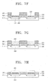
- FIG. 7A through FIG. 7H are cross-sectional views taken along lines III-III of FIG. 6A through FIG. 6H, respectively.
- the magnetic field detecting element manufactured according to the manufacturing method of the present invention comprises: a semiconductor substrate 200; a soft magnetic core 220; the first and the second insulating films 230, 240 positioned at the upper and the lower parts of the soft magnetic core 220; and the first and the second coils 250, 260 formed in such a way that those coils enclose the soft magnetic core 220 with the soft magnetic core 220 and the insulating films 230, 240 intervened, and having a plurality of coil lines 251, 252,..., 261, 262,..., respectively.
- the first coil 250 is positioned on the lower side of the soft magnetic core 220, and the second coil 260 is positioned on the upper side of the soft magnetic core 220.
- the semiconductor substrate 200 has an approximately rectangular well 211 that collapses in a predetermined depth D from its surface and the first coil 250 is arranged in the inside of that well 211 so that the first coil 250 may not be exposed to the surface of the semiconductor substrate 200 according to the characteristics of the present invention.
- the height H of a plurality of the coil lines 51 constituting the first coil 250 formed in the inside of the well 211 is the same as the depth of the well 211. Therefore, the upper surface of the coil lines 251 maintains the same plane as the upper surface of the semiconductor substrate 200.
- the first coil 250 is not projected to the surface of the semiconductor substrate 200 but is formed in the same plane as the upper surface of the semiconductor substrate 200 in the inside of the well 211 of the semiconductor substrate 200, it is easy to perform planarization of the semiconductor substrate 200 in which the first coil 250 is formed and it is possible to make very thin the thickness of a planarization material, for example, the insulating films 230, 240.
- the approximately rectangular well 211 is formed in such a way that the well has an inclined sidewall that is gradually inclined in its inside from its upper part to its bottom and may be formed by a variety of the etching technologies generally well known.
- the first and the second coils 250, 260 are connected, by means of a third coil 300 filled upon formation of the second coil 260, to through holes 290, 290' formed on both ends of the soft magnetic core 220 by passing through the first and the second insulating films 230, 240.
- FIG. 6A and FIG. 7A are cross-sectional views showing that a first plating mold 270 for forming the first coil 250 is formed on the upper surface of the semiconductor substrate 200 in which the well 211 is formed.
- a seed film for plating is formed on the surface of the well 211, and the first plating mold 270 is formed by exposing and developing processes after the photoresist is spread thick on the seed film.
- the reference numeral 270a is a groove of the first plating mold 270.
- the first coil 250 as shown in FIG. 6B and FIG. 7B is formed on the well 211 of the semiconductor substrate 200.
- the first coil 250 does not project beyond the surface of the semiconductor substrate 200 but formed in the same plane as the semiconductor substrate 200.
- an insulating material is spread on the upper surface of the semiconductor substrate 200 in which the first coil 250 is formed, so that a first insulating film 230 for planarization and insulation, is formed. Since the first coil 250 does not project beyond the surface of the semiconductor substrate 200 but maintains the same plane as the semiconductor substrate, it is easy to perform planarization and it is possible to make the insulating film 230 very thin as well.
- a soft magnetic material film is stacked on the first insulating film 230 and a soft magnetic core 220 is formed by pattern formation and etching as shown in FIG. 6D and FIG. 7D.
- an insulating material is spread in a predetermined thickness, on the upper part of the first insulating film 230 including the soft magnetic core 220 so that a second insulating film 240 as shown in FIG. 6E and FIG. 7E is formed.
- the portions that correspond to the both ends of the soft magnetic core 220 of the second insulating film 240 are etched so that the through holes 290, 290' as shown in FIG 7F are formed, and the process for forming the second coil 260 is proceeded. Since the thickness of the first and the second insulating films 230, 240 is formed very thin according to the characteristics of the present invention upon etching for formation of the through holes 290, 290', the etching process could be performed in a simple manner. Also, since it is possible to realize the fine-pitched coils due to such simplification of the process, the sensor of high sensitivity is possibly manufactured.
- the formation of the second coil 260 is performed in such a way that firstly the seed film (not shown) is formed on the upper surface of the second insulating film 240 in which the through holes 290, 290' are formed, and the photoresist is spread on that seed film, then the second plating mold 280 having a plurality of grooves 280a is formed by exposing and developing processes as shown in FIG. 6F and FIG 7F.
- metal is filled in the groove 280a of the plating mold 280 by means of the electric plating method so that a coil line 261 is formed as shown in FIG. 6G and FIG. 7G
- metal is filled in the through holes 290, 290', whereby the first coil 250 at the lower side is connected to the second coil 260 at the upper side by means of a third coil 300 that is filled in the through holes 290, 290'. Therefore, the coils 250, 260 are realized in such a way that these coils enclose the soft magnetic core 220.
- the magnetic field detecting element manufactured by the present invention could reduce the whole height of the element as much as the depth of the well 211 formed on the semiconductor substrate 200, thus a thin structure is possibly realized.
- a protection film for protecting the structures formed thereon could be formed.
- the first coil is not projected to the upper part of the semiconductor substrate but positioned in the inside of the well, it is easy to perform planarization of the semiconductor substrate and it is possible to make thin the thickness of the planarization material as well. Therefore, performance improvement of the soft magnetic core is expected thanks to improvement in planarization degree, and simplification of the etching process for forming the through hole is expected thanks to realization of the thin insulating film. Also, the pitch between the coils could be reduced thanks to simplification of the etching process, thus the sensitivity of the sensor could be improved.
- manufacturing of the magnetic field detecting element is simplified, whereby productivity improvement is expected and the thin-type element of good sensitivity is possibly manufactured as well.
Landscapes
- Physics & Mathematics (AREA)
- Condensed Matter Physics & Semiconductors (AREA)
- General Physics & Mathematics (AREA)
- Engineering & Computer Science (AREA)
- Power Engineering (AREA)
- Manufacturing & Machinery (AREA)
- Measuring Magnetic Variables (AREA)
- Semiconductor Integrated Circuits (AREA)
- Manufacturing Cores, Coils, And Magnets (AREA)
- Geophysics And Detection Of Objects (AREA)
- Hall/Mr Elements (AREA)
Priority Applications (1)
| Application Number | Priority Date | Filing Date | Title |
|---|---|---|---|
| EP05076754A EP1602936B1 (de) | 2003-02-25 | 2004-02-24 | Verfahren zur Herstellung eines Magnetfelddetektors |
Applications Claiming Priority (4)
| Application Number | Priority Date | Filing Date | Title |
|---|---|---|---|
| KR2003011807 | 2003-02-25 | ||
| KR1020030011807A KR100546880B1 (ko) | 2003-02-25 | 2003-02-25 | 미세 자계검출소자의 제조방법 |
| KR2003034191 | 2003-05-28 | ||
| KR10-2003-0034191A KR100518796B1 (ko) | 2003-05-28 | 2003-05-28 | 자계검출소자 및 그 제조방법 |
Related Child Applications (1)
| Application Number | Title | Priority Date | Filing Date |
|---|---|---|---|
| EP05076754A Division EP1602936B1 (de) | 2003-02-25 | 2004-02-24 | Verfahren zur Herstellung eines Magnetfelddetektors |
Publications (3)
| Publication Number | Publication Date |
|---|---|
| EP1467216A2 true EP1467216A2 (de) | 2004-10-13 |
| EP1467216A3 EP1467216A3 (de) | 2005-01-26 |
| EP1467216B1 EP1467216B1 (de) | 2007-06-13 |
Family
ID=36567864
Family Applications (2)
| Application Number | Title | Priority Date | Filing Date |
|---|---|---|---|
| EP04251015A Expired - Lifetime EP1467216B1 (de) | 2003-02-25 | 2004-02-24 | Verfahren zur Herstellung eines Magnetfelddetektors |
| EP05076754A Expired - Lifetime EP1602936B1 (de) | 2003-02-25 | 2004-02-24 | Verfahren zur Herstellung eines Magnetfelddetektors |
Family Applications After (1)
| Application Number | Title | Priority Date | Filing Date |
|---|---|---|---|
| EP05076754A Expired - Lifetime EP1602936B1 (de) | 2003-02-25 | 2004-02-24 | Verfahren zur Herstellung eines Magnetfelddetektors |
Country Status (5)
| Country | Link |
|---|---|
| US (2) | US7041526B2 (de) |
| EP (2) | EP1467216B1 (de) |
| JP (2) | JP2004258038A (de) |
| AT (1) | ATE364846T1 (de) |
| DE (1) | DE602004006905T2 (de) |
Cited By (1)
| Publication number | Priority date | Publication date | Assignee | Title |
|---|---|---|---|---|
| EP1783789A1 (de) * | 2005-09-30 | 2007-05-09 | TDK Corporation | Dünnfilmvorrichtung und Dünnfilmspule |
Families Citing this family (19)
| Publication number | Priority date | Publication date | Assignee | Title |
|---|---|---|---|---|
| KR100662610B1 (ko) * | 2005-01-25 | 2007-01-02 | 삼성전자주식회사 | 자계검출소자 및 그 제조방법 |
| JP2009535616A (ja) * | 2006-04-28 | 2009-10-01 | マイクロゲート インコーポレイテッド | 薄膜型3軸フラックスゲート及びその製造方法 |
| US8044755B2 (en) * | 2008-04-09 | 2011-10-25 | National Semiconductor Corporation | MEMS power inductor |
| US7705411B2 (en) * | 2008-04-09 | 2010-04-27 | National Semiconductor Corporation | MEMS-topped integrated circuit with a stress relief layer |
| JP4725600B2 (ja) * | 2008-06-10 | 2011-07-13 | 愛知製鋼株式会社 | マグネトインピーダンスセンサ素子 |
| RU2421747C1 (ru) * | 2010-01-11 | 2011-06-20 | Олег Фёдорович Меньших | Прибор для исследования магнитного силового взаимодействия |
| US8558344B2 (en) * | 2011-09-06 | 2013-10-15 | Analog Devices, Inc. | Small size and fully integrated power converter with magnetics on chip |
| US20130106552A1 (en) * | 2011-11-02 | 2013-05-02 | International Business Machines Corporation | Inductor with multiple polymeric layers |
| US9064628B2 (en) | 2012-05-22 | 2015-06-23 | International Business Machines Corporation | Inductor with stacked conductors |
| RU2539290C2 (ru) * | 2013-05-21 | 2015-01-20 | Олег Фёдорович Меньших | Устройство для исследования магнитного трения |
| US20170234942A1 (en) * | 2016-02-11 | 2017-08-17 | Texas Instruments Incorporated | Layouts for interlevel crack prevention in fluxgate technology manufacturing |
| KR101952872B1 (ko) * | 2017-06-23 | 2019-05-17 | 삼성전기주식회사 | 코일 부품 및 그의 제조방법 |
| WO2019018925A1 (en) * | 2017-07-25 | 2019-01-31 | Tsafaridis, Demetrius | MULTILAYER THIN FILM SENSOR FOR NON-DESTRUCTIVE TESTING OF FERROMAGNETIC MATERIALS |
| TWI798287B (zh) * | 2017-12-08 | 2023-04-11 | 日商日本電產理德股份有限公司 | Mi元件的製造方法及mi元件 |
| KR102096760B1 (ko) | 2018-07-04 | 2020-04-03 | 스템코 주식회사 | 코일 장치 및 그 제조 방법 |
| JP7203400B1 (ja) | 2022-10-17 | 2023-01-13 | マグネデザイン株式会社 | Gsr素子の製造方法 |
| WO2024085098A1 (ja) * | 2022-10-17 | 2024-04-25 | マグネデザイン株式会社 | Gsr素子の製造方法 |
| JP7207676B1 (ja) | 2022-10-17 | 2023-01-18 | マグネデザイン株式会社 | Gsr素子の製造方法 |
| JP7201194B1 (ja) | 2022-10-17 | 2023-01-10 | マグネデザイン株式会社 | 磁界検出素子の製造方法 |
Family Cites Families (18)
| Publication number | Priority date | Publication date | Assignee | Title |
|---|---|---|---|---|
| JPS5246787A (en) * | 1975-10-11 | 1977-04-13 | Hitachi Ltd | Coil for integrated circuit and process for production of same |
| DE3420709A1 (de) * | 1984-06-02 | 1985-12-05 | Robert Bosch Gmbh, 7000 Stuttgart | Magnetfeldsensor zur messung der feldstaerke eines magnetfeldes und verfahren zu seiner herstellung |
| US5070317A (en) * | 1989-01-17 | 1991-12-03 | Bhagat Jayant K | Miniature inductor for integrated circuits and devices |
| JP3093813B2 (ja) * | 1991-03-29 | 2000-10-03 | 科学技術振興事業団 | 磁気センサ |
| DE4220186A1 (de) | 1992-06-19 | 1993-12-23 | Schaltbau Ag | Meßschaltung für Magnetfelder |
| JP3545074B2 (ja) * | 1994-12-27 | 2004-07-21 | 独立行政法人 科学技術振興機構 | 半導体基板に集積される磁気検出素子及び磁気検出モジュール |
| KR100250225B1 (ko) * | 1996-11-19 | 2000-04-01 | 윤종용 | 집적회로용 인덕터 및 그 제조방법 |
| JP3600415B2 (ja) | 1997-07-15 | 2004-12-15 | 株式会社東芝 | 分布定数素子 |
| US6030877A (en) * | 1997-10-06 | 2000-02-29 | Industrial Technology Research Institute | Electroless gold plating method for forming inductor structures |
| US6166422A (en) * | 1998-05-13 | 2000-12-26 | Lsi Logic Corporation | Inductor with cobalt/nickel core for integrated circuit structure with high inductance and high Q-factor |
| KR100480749B1 (ko) | 1998-07-07 | 2005-09-30 | 삼성전자주식회사 | 차동 솔레노이드형 자계검출소자 및 그 제조방법 |
| KR100468833B1 (ko) | 1998-07-28 | 2005-03-16 | 삼성전자주식회사 | 차동스파이어럴형자계검출소자및이를채용한자계검출모듈 |
| WO2000062314A1 (en) * | 1999-04-14 | 2000-10-19 | Takashi Nishi | Microsolenoid coil and its manufacturing method |
| US6835576B2 (en) * | 2000-05-02 | 2004-12-28 | Fuji Electric Co., Ltd. | Magnetic thin film, a magnetic component that uses this magnetic thin film, manufacturing methods for the same, and a power conversion device |
| KR100464097B1 (ko) | 2002-03-14 | 2005-01-03 | 삼성전자주식회사 | 반도체기판에 집적된 자계검출소자 및 그 제조방법 |
| KR100544475B1 (ko) | 2003-01-25 | 2006-01-24 | 삼성전자주식회사 | 반도체기판에 집적된 자계검출소자 및 그 제조방법 |
| KR100536837B1 (ko) | 2003-02-10 | 2005-12-16 | 삼성전자주식회사 | 반도체기판에 집적된 자계검출소자 및 그 제조방법 |
| US7191639B2 (en) * | 2003-04-08 | 2007-03-20 | California Institute Of Technology | On-chip magnetic force actuation of microcantilevers by coplanar coils |
-
2004
- 2004-02-23 US US10/784,479 patent/US7041526B2/en not_active Expired - Lifetime
- 2004-02-24 DE DE602004006905T patent/DE602004006905T2/de not_active Expired - Lifetime
- 2004-02-24 EP EP04251015A patent/EP1467216B1/de not_active Expired - Lifetime
- 2004-02-24 EP EP05076754A patent/EP1602936B1/de not_active Expired - Lifetime
- 2004-02-24 AT AT04251015T patent/ATE364846T1/de not_active IP Right Cessation
- 2004-02-25 JP JP2004050236A patent/JP2004258038A/ja active Pending
-
2006
- 2006-01-23 US US11/336,881 patent/US20060115918A1/en not_active Abandoned
-
2007
- 2007-09-12 JP JP2007236186A patent/JP4633096B2/ja not_active Expired - Fee Related
Cited By (1)
| Publication number | Priority date | Publication date | Assignee | Title |
|---|---|---|---|---|
| EP1783789A1 (de) * | 2005-09-30 | 2007-05-09 | TDK Corporation | Dünnfilmvorrichtung und Dünnfilmspule |
Also Published As
| Publication number | Publication date |
|---|---|
| JP2004258038A (ja) | 2004-09-16 |
| EP1602936A1 (de) | 2005-12-07 |
| EP1467216A3 (de) | 2005-01-26 |
| EP1602936B1 (de) | 2012-06-06 |
| ATE364846T1 (de) | 2007-07-15 |
| US20050006713A1 (en) | 2005-01-13 |
| DE602004006905T2 (de) | 2008-02-07 |
| US7041526B2 (en) | 2006-05-09 |
| JP2008003105A (ja) | 2008-01-10 |
| JP4633096B2 (ja) | 2011-02-16 |
| US20060115918A1 (en) | 2006-06-01 |
| DE602004006905D1 (de) | 2007-07-26 |
| EP1467216B1 (de) | 2007-06-13 |
Similar Documents
| Publication | Publication Date | Title |
|---|---|---|
| EP1467216B1 (de) | Verfahren zur Herstellung eines Magnetfelddetektors | |
| US7338816B2 (en) | Magnetic field sensing device and a fabricating method of the same | |
| JP3839452B2 (ja) | 金属構造物の製造方法 | |
| JP2004253684A (ja) | 高密度インダクタおよびその製造方法 | |
| TWI578547B (zh) | 電磁阻抗感測元件及其製作方法 | |
| US6990725B2 (en) | Fabrication approaches for the formation of planar inductors and transformers | |
| US6888213B2 (en) | Dielectric insulation structure for integrating electronic semiconductor devices and relevant manufacturing process | |
| JPH0290617A (ja) | 半導体装置の製造方法 | |
| JPH11111926A (ja) | 半導体素子のインダクタ製造方法 | |
| KR100518796B1 (ko) | 자계검출소자 및 그 제조방법 | |
| JP3770871B2 (ja) | Mems構造物及びその作製方法 | |
| KR100611474B1 (ko) | 반도체 소자의 인덕터 제조 방법 | |
| JP2006278484A (ja) | コイル部品、及びコイル部品の製造方法 | |
| JP2003133148A (ja) | 巻線型コモンモードチョークコイル及びその製造方法 | |
| TWI545332B (zh) | 電磁阻抗感測元件及其製作方法 | |
| JPS5935165B2 (ja) | 多層薄膜コイルの製法 | |
| KR100528795B1 (ko) | 반도체 소자의 인덕터 제조 방법 | |
| KR100367621B1 (ko) | 자기수동소자의 제조방법 | |
| JPH05151525A (ja) | 薄膜磁気ヘツドの製造方法 | |
| JP2001210571A (ja) | アライメントマークの形成方法 | |
| JPS61287142A (ja) | 誘電体分離基板の製造方法 | |
| JPH08194918A (ja) | 薄膜磁気ヘッド | |
| JPH02143905A (ja) | 薄膜磁気ヘッドの製造方法 | |
| KR20000061325A (ko) | 인덕터 제조방법 | |
| JPS61178711A (ja) | 薄膜磁気ヘツド |
Legal Events
| Date | Code | Title | Description |
|---|---|---|---|
| PUAI | Public reference made under article 153(3) epc to a published international application that has entered the european phase |
Free format text: ORIGINAL CODE: 0009012 |
|
| AK | Designated contracting states |
Kind code of ref document: A2 Designated state(s): AT BE BG CH CY CZ DE DK EE ES FI FR GB GR HU IE IT LI LU MC NL PT RO SE SI SK TR |
|
| AX | Request for extension of the european patent |
Extension state: AL HR LT LV MK |
|
| PUAL | Search report despatched |
Free format text: ORIGINAL CODE: 0009013 |
|
| AK | Designated contracting states |
Kind code of ref document: A3 Designated state(s): AT BE BG CH CY CZ DE DK EE ES FI FR GB GR HU IE IT LI LU MC NL PT RO SE SI SK TR |
|
| AX | Request for extension of the european patent |
Extension state: AL HR LT LV MK |
|
| RIC1 | Information provided on ipc code assigned before grant |
Ipc: 7G 01R 33/02 B Ipc: 7G 01R 33/04 B Ipc: 7G 01R 33/028 A Ipc: 7H 01L 43/00 B |
|
| 17P | Request for examination filed |
Effective date: 20050223 |
|
| 17Q | First examination report despatched |
Effective date: 20050322 |
|
| AKX | Designation fees paid |
Designated state(s): AT BE BG CH CY CZ DE DK EE ES FI FR GB GR HU IE IT LI LU MC NL PT RO SE SI SK TR |
|
| GRAP | Despatch of communication of intention to grant a patent |
Free format text: ORIGINAL CODE: EPIDOSNIGR1 |
|
| GRAS | Grant fee paid |
Free format text: ORIGINAL CODE: EPIDOSNIGR3 |
|
| GRAA | (expected) grant |
Free format text: ORIGINAL CODE: 0009210 |
|
| AK | Designated contracting states |
Kind code of ref document: B1 Designated state(s): AT BE BG CH CY CZ DE DK EE ES FI FR GB GR HU IE IT LI LU MC NL PT RO SE SI SK TR |
|
| PG25 | Lapsed in a contracting state [announced via postgrant information from national office to epo] |
Ref country code: LI Free format text: LAPSE BECAUSE OF FAILURE TO SUBMIT A TRANSLATION OF THE DESCRIPTION OR TO PAY THE FEE WITHIN THE PRESCRIBED TIME-LIMIT Effective date: 20070613 Ref country code: CH Free format text: LAPSE BECAUSE OF FAILURE TO SUBMIT A TRANSLATION OF THE DESCRIPTION OR TO PAY THE FEE WITHIN THE PRESCRIBED TIME-LIMIT Effective date: 20070613 |
|
| REG | Reference to a national code |
Ref country code: GB Ref legal event code: FG4D |
|
| REG | Reference to a national code |
Ref country code: CH Ref legal event code: EP |
|
| REG | Reference to a national code |
Ref country code: IE Ref legal event code: FG4D |
|
| REF | Corresponds to: |
Ref document number: 602004006905 Country of ref document: DE Date of ref document: 20070726 Kind code of ref document: P |
|
| PG25 | Lapsed in a contracting state [announced via postgrant information from national office to epo] |
Ref country code: SE Free format text: LAPSE BECAUSE OF FAILURE TO SUBMIT A TRANSLATION OF THE DESCRIPTION OR TO PAY THE FEE WITHIN THE PRESCRIBED TIME-LIMIT Effective date: 20070913 |
|
| ET | Fr: translation filed | ||
| PG25 | Lapsed in a contracting state [announced via postgrant information from national office to epo] |
Ref country code: AT Free format text: LAPSE BECAUSE OF FAILURE TO SUBMIT A TRANSLATION OF THE DESCRIPTION OR TO PAY THE FEE WITHIN THE PRESCRIBED TIME-LIMIT Effective date: 20070613 |
|
| NLV1 | Nl: lapsed or annulled due to failure to fulfill the requirements of art. 29p and 29m of the patents act | ||
| REG | Reference to a national code |
Ref country code: CH Ref legal event code: PL |
|
| PG25 | Lapsed in a contracting state [announced via postgrant information from national office to epo] |
Ref country code: BE Free format text: LAPSE BECAUSE OF FAILURE TO SUBMIT A TRANSLATION OF THE DESCRIPTION OR TO PAY THE FEE WITHIN THE PRESCRIBED TIME-LIMIT Effective date: 20070613 |
|
| PG25 | Lapsed in a contracting state [announced via postgrant information from national office to epo] |
Ref country code: SI Free format text: LAPSE BECAUSE OF FAILURE TO SUBMIT A TRANSLATION OF THE DESCRIPTION OR TO PAY THE FEE WITHIN THE PRESCRIBED TIME-LIMIT Effective date: 20070613 Ref country code: PT Free format text: LAPSE BECAUSE OF FAILURE TO SUBMIT A TRANSLATION OF THE DESCRIPTION OR TO PAY THE FEE WITHIN THE PRESCRIBED TIME-LIMIT Effective date: 20071113 Ref country code: ES Free format text: LAPSE BECAUSE OF FAILURE TO SUBMIT A TRANSLATION OF THE DESCRIPTION OR TO PAY THE FEE WITHIN THE PRESCRIBED TIME-LIMIT Effective date: 20070924 Ref country code: CZ Free format text: LAPSE BECAUSE OF FAILURE TO SUBMIT A TRANSLATION OF THE DESCRIPTION OR TO PAY THE FEE WITHIN THE PRESCRIBED TIME-LIMIT Effective date: 20070613 Ref country code: NL Free format text: LAPSE BECAUSE OF FAILURE TO SUBMIT A TRANSLATION OF THE DESCRIPTION OR TO PAY THE FEE WITHIN THE PRESCRIBED TIME-LIMIT Effective date: 20070613 Ref country code: BG Free format text: LAPSE BECAUSE OF FAILURE TO SUBMIT A TRANSLATION OF THE DESCRIPTION OR TO PAY THE FEE WITHIN THE PRESCRIBED TIME-LIMIT Effective date: 20070913 |
|
| PG25 | Lapsed in a contracting state [announced via postgrant information from national office to epo] |
Ref country code: SK Free format text: LAPSE BECAUSE OF FAILURE TO SUBMIT A TRANSLATION OF THE DESCRIPTION OR TO PAY THE FEE WITHIN THE PRESCRIBED TIME-LIMIT Effective date: 20070613 |
|
| PLBE | No opposition filed within time limit |
Free format text: ORIGINAL CODE: 0009261 |
|
| STAA | Information on the status of an ep patent application or granted ep patent |
Free format text: STATUS: NO OPPOSITION FILED WITHIN TIME LIMIT |
|
| PG25 | Lapsed in a contracting state [announced via postgrant information from national office to epo] |
Ref country code: IT Free format text: LAPSE BECAUSE OF FAILURE TO SUBMIT A TRANSLATION OF THE DESCRIPTION OR TO PAY THE FEE WITHIN THE PRESCRIBED TIME-LIMIT Effective date: 20070613 Ref country code: GR Free format text: LAPSE BECAUSE OF FAILURE TO SUBMIT A TRANSLATION OF THE DESCRIPTION OR TO PAY THE FEE WITHIN THE PRESCRIBED TIME-LIMIT Effective date: 20070914 Ref country code: DK Free format text: LAPSE BECAUSE OF FAILURE TO SUBMIT A TRANSLATION OF THE DESCRIPTION OR TO PAY THE FEE WITHIN THE PRESCRIBED TIME-LIMIT Effective date: 20070613 |
|
| 26N | No opposition filed |
Effective date: 20080314 |
|
| PG25 | Lapsed in a contracting state [announced via postgrant information from national office to epo] |
Ref country code: RO Free format text: LAPSE BECAUSE OF FAILURE TO SUBMIT A TRANSLATION OF THE DESCRIPTION OR TO PAY THE FEE WITHIN THE PRESCRIBED TIME-LIMIT Effective date: 20070613 |
|
| PG25 | Lapsed in a contracting state [announced via postgrant information from national office to epo] |
Ref country code: MC Free format text: LAPSE BECAUSE OF NON-PAYMENT OF DUE FEES Effective date: 20080228 |
|
| PG25 | Lapsed in a contracting state [announced via postgrant information from national office to epo] |
Ref country code: IE Free format text: LAPSE BECAUSE OF NON-PAYMENT OF DUE FEES Effective date: 20080225 Ref country code: EE Free format text: LAPSE BECAUSE OF FAILURE TO SUBMIT A TRANSLATION OF THE DESCRIPTION OR TO PAY THE FEE WITHIN THE PRESCRIBED TIME-LIMIT Effective date: 20070613 |
|
| PG25 | Lapsed in a contracting state [announced via postgrant information from national office to epo] |
Ref country code: FI Free format text: LAPSE BECAUSE OF FAILURE TO SUBMIT A TRANSLATION OF THE DESCRIPTION OR TO PAY THE FEE WITHIN THE PRESCRIBED TIME-LIMIT Effective date: 20070613 |
|
| PG25 | Lapsed in a contracting state [announced via postgrant information from national office to epo] |
Ref country code: CY Free format text: LAPSE BECAUSE OF FAILURE TO SUBMIT A TRANSLATION OF THE DESCRIPTION OR TO PAY THE FEE WITHIN THE PRESCRIBED TIME-LIMIT Effective date: 20070613 |
|
| PG25 | Lapsed in a contracting state [announced via postgrant information from national office to epo] |
Ref country code: HU Free format text: LAPSE BECAUSE OF FAILURE TO SUBMIT A TRANSLATION OF THE DESCRIPTION OR TO PAY THE FEE WITHIN THE PRESCRIBED TIME-LIMIT Effective date: 20071214 Ref country code: LU Free format text: LAPSE BECAUSE OF NON-PAYMENT OF DUE FEES Effective date: 20080224 |
|
| PG25 | Lapsed in a contracting state [announced via postgrant information from national office to epo] |
Ref country code: TR Free format text: LAPSE BECAUSE OF FAILURE TO SUBMIT A TRANSLATION OF THE DESCRIPTION OR TO PAY THE FEE WITHIN THE PRESCRIBED TIME-LIMIT Effective date: 20070613 |
|
| REG | Reference to a national code |
Ref country code: FR Ref legal event code: PLFP Year of fee payment: 13 |
|
| REG | Reference to a national code |
Ref country code: FR Ref legal event code: PLFP Year of fee payment: 14 |
|
| REG | Reference to a national code |
Ref country code: FR Ref legal event code: PLFP Year of fee payment: 15 |
|
| PGFP | Annual fee paid to national office [announced via postgrant information from national office to epo] |
Ref country code: DE Payment date: 20200121 Year of fee payment: 17 Ref country code: GB Payment date: 20200123 Year of fee payment: 17 |
|
| PGFP | Annual fee paid to national office [announced via postgrant information from national office to epo] |
Ref country code: FR Payment date: 20200123 Year of fee payment: 17 |
|
| REG | Reference to a national code |
Ref country code: DE Ref legal event code: R119 Ref document number: 602004006905 Country of ref document: DE |
|
| GBPC | Gb: european patent ceased through non-payment of renewal fee |
Effective date: 20210224 |
|
| PG25 | Lapsed in a contracting state [announced via postgrant information from national office to epo] |
Ref country code: GB Free format text: LAPSE BECAUSE OF NON-PAYMENT OF DUE FEES Effective date: 20210224 Ref country code: FR Free format text: LAPSE BECAUSE OF NON-PAYMENT OF DUE FEES Effective date: 20210228 Ref country code: DE Free format text: LAPSE BECAUSE OF NON-PAYMENT OF DUE FEES Effective date: 20210901 |