EP1467410A2 - Aktiver Pixelsensor mit Unterdrückung von Reset-Räuschen und programmierbarer Pixelzusammenfassungen - Google Patents
Aktiver Pixelsensor mit Unterdrückung von Reset-Räuschen und programmierbarer Pixelzusammenfassungen Download PDFInfo
- Publication number
- EP1467410A2 EP1467410A2 EP04368002A EP04368002A EP1467410A2 EP 1467410 A2 EP1467410 A2 EP 1467410A2 EP 04368002 A EP04368002 A EP 04368002A EP 04368002 A EP04368002 A EP 04368002A EP 1467410 A2 EP1467410 A2 EP 1467410A2
- Authority
- EP
- European Patent Office
- Prior art keywords
- pixel cells
- binning
- well pixel
- wells
- well
- Prior art date
- Legal status (The legal status is an assumption and is not a legal conclusion. Google has not performed a legal analysis and makes no representation as to the accuracy of the status listed.)
- Withdrawn
Links
Images


Classifications
-
- H—ELECTRICITY
- H10—SEMICONDUCTOR DEVICES; ELECTRIC SOLID-STATE DEVICES NOT OTHERWISE PROVIDED FOR
- H10F—INORGANIC SEMICONDUCTOR DEVICES SENSITIVE TO INFRARED RADIATION, LIGHT, ELECTROMAGNETIC RADIATION OF SHORTER WAVELENGTH OR CORPUSCULAR RADIATION
- H10F99/00—Subject matter not provided for in other groups of this subclass
-
- H—ELECTRICITY
- H10—SEMICONDUCTOR DEVICES; ELECTRIC SOLID-STATE DEVICES NOT OTHERWISE PROVIDED FOR
- H10F—INORGANIC SEMICONDUCTOR DEVICES SENSITIVE TO INFRARED RADIATION, LIGHT, ELECTROMAGNETIC RADIATION OF SHORTER WAVELENGTH OR CORPUSCULAR RADIATION
- H10F39/00—Integrated devices, or assemblies of multiple devices, comprising at least one element covered by group H10F30/00, e.g. radiation detectors comprising photodiode arrays
- H10F39/80—Constructional details of image sensors
- H10F39/802—Geometry or disposition of elements in pixels, e.g. address-lines or gate electrodes
-
- H—ELECTRICITY
- H04—ELECTRIC COMMUNICATION TECHNIQUE
- H04N—PICTORIAL COMMUNICATION, e.g. TELEVISION
- H04N25/00—Circuitry of solid-state image sensors [SSIS]; Control thereof
- H04N25/40—Extracting pixel data from image sensors by controlling scanning circuits, e.g. by modifying the number of pixels sampled or to be sampled
- H04N25/46—Extracting pixel data from image sensors by controlling scanning circuits, e.g. by modifying the number of pixels sampled or to be sampled by combining or binning pixels
-
- H—ELECTRICITY
- H04—ELECTRIC COMMUNICATION TECHNIQUE
- H04N—PICTORIAL COMMUNICATION, e.g. TELEVISION
- H04N25/00—Circuitry of solid-state image sensors [SSIS]; Control thereof
- H04N25/60—Noise processing, e.g. detecting, correcting, reducing or removing noise
- H04N25/617—Noise processing, e.g. detecting, correcting, reducing or removing noise for reducing electromagnetic interference, e.g. clocking noise
-
- H—ELECTRICITY
- H04—ELECTRIC COMMUNICATION TECHNIQUE
- H04N—PICTORIAL COMMUNICATION, e.g. TELEVISION
- H04N25/00—Circuitry of solid-state image sensors [SSIS]; Control thereof
- H04N25/60—Noise processing, e.g. detecting, correcting, reducing or removing noise
- H04N25/65—Noise processing, e.g. detecting, correcting, reducing or removing noise applied to reset noise, e.g. KTC noise related to CMOS structures by techniques other than CDS
-
- H—ELECTRICITY
- H04—ELECTRIC COMMUNICATION TECHNIQUE
- H04N—PICTORIAL COMMUNICATION, e.g. TELEVISION
- H04N25/00—Circuitry of solid-state image sensors [SSIS]; Control thereof
- H04N25/70—SSIS architectures; Circuits associated therewith
- H04N25/76—Addressed sensors, e.g. MOS or CMOS sensors
-
- H—ELECTRICITY
- H04—ELECTRIC COMMUNICATION TECHNIQUE
- H04N—PICTORIAL COMMUNICATION, e.g. TELEVISION
- H04N25/00—Circuitry of solid-state image sensors [SSIS]; Control thereof
- H04N25/70—SSIS architectures; Circuits associated therewith
- H04N25/76—Addressed sensors, e.g. MOS or CMOS sensors
- H04N25/77—Pixel circuitry, e.g. memories, A/D converters, pixel amplifiers, shared circuits or shared components
- H04N25/778—Pixel circuitry, e.g. memories, A/D converters, pixel amplifiers, shared circuits or shared components comprising amplifiers shared between a plurality of pixels, i.e. at least one part of the amplifier must be on the sensor array itself
-
- H—ELECTRICITY
- H10—SEMICONDUCTOR DEVICES; ELECTRIC SOLID-STATE DEVICES NOT OTHERWISE PROVIDED FOR
- H10F—INORGANIC SEMICONDUCTOR DEVICES SENSITIVE TO INFRARED RADIATION, LIGHT, ELECTROMAGNETIC RADIATION OF SHORTER WAVELENGTH OR CORPUSCULAR RADIATION
- H10F30/00—Individual radiation-sensitive semiconductor devices in which radiation controls the flow of current through the devices, e.g. photodetectors
- H10F30/20—Individual radiation-sensitive semiconductor devices in which radiation controls the flow of current through the devices, e.g. photodetectors the devices having potential barriers, e.g. phototransistors
-
- H—ELECTRICITY
- H10—SEMICONDUCTOR DEVICES; ELECTRIC SOLID-STATE DEVICES NOT OTHERWISE PROVIDED FOR
- H10F—INORGANIC SEMICONDUCTOR DEVICES SENSITIVE TO INFRARED RADIATION, LIGHT, ELECTROMAGNETIC RADIATION OF SHORTER WAVELENGTH OR CORPUSCULAR RADIATION
- H10F39/00—Integrated devices, or assemblies of multiple devices, comprising at least one element covered by group H10F30/00, e.g. radiation detectors comprising photodiode arrays
- H10F39/80—Constructional details of image sensors
- H10F39/803—Pixels having integrated switching, control, storage or amplification elements
-
- H—ELECTRICITY
- H10—SEMICONDUCTOR DEVICES; ELECTRIC SOLID-STATE DEVICES NOT OTHERWISE PROVIDED FOR
- H10F—INORGANIC SEMICONDUCTOR DEVICES SENSITIVE TO INFRARED RADIATION, LIGHT, ELECTROMAGNETIC RADIATION OF SHORTER WAVELENGTH OR CORPUSCULAR RADIATION
- H10F39/00—Integrated devices, or assemblies of multiple devices, comprising at least one element covered by group H10F30/00, e.g. radiation detectors comprising photodiode arrays
- H10F39/10—Integrated devices
- H10F39/12—Image sensors
- H10F39/18—Complementary metal-oxide-semiconductor [CMOS] image sensors; Photodiode array image sensors
Definitions
- This invention relates to a circuit and method for suppressing noise during pixel reset and more specifically to using programmable binning to selectively bin adjacent pixels during reset.
- U.S. Pat. No. 6,424,750 B1 to Colbeth et al. describes an X-Ray imaging system.
- pixel binning is used to combine pixel information collected by the detector array.
- U.S. Pat. No. 5,848,123 to Strommer describes methods and apparatus for imaging an object by detecting radiation reflected from and/or transmitted through the object using an imaging sensor system.
- the sensor system is configured by means of a control scheme based on combining or binning the imaging elements.
- a circuit having a number of N-wells formed in a P - silicon epitaxial layer.
- a pixel is formed in each of the N - wells so that each of the N - wells is surrounded by P - type silicon and an array of pixels is formed.
- Means are provided for selectively combining or binning adjacent N - wells. During the reset period of the imaging cycle selected groups of adjacent pixels are binned and the charge injected by the resetting of a pixel is averaged among the neighboring pixels, thereby reducing the effect of this charge injection on any one of the pixels and thus reducing the noise generated.
- One means for binning the pixels is to connect selected N - wells with selected adjacent N- wells using traces of conductive material formed over the P-regions between the selected N- wells. This electrically connects or bins the selected adjacent N - wells.
- Another method of binning pixels is to form N + channel regions between the selected adjacent N - wells followed by forming a gate dielectric and gate electrode over the N + channel regions. This forms an N channel metal oxide semiconductor, NMOS, transistor which can be used to connect or disconnect the selected adjacent N - wells as desired by turning the NMOS transistors on or off.
- a circuit having a number of P - wells formed in an N - silicon epitaxial layer.
- a pixel is formed in each of the P - wells so that each of the P - wells is surrounded by N - type silicon and an array of pixels is formed.
- Means are provided for selectively combining or binning adjacent P - wells. During the reset period of the imaging cycle selected groups of adjacent pixels are binned and the charge injected by the resetting of a pixel is averaged among the neighboring pixels, thereby reducing the effect of this charge injection on any one of the pixels and thus reducing the noise generated.
- One means for binning the pixels is to connect selected P - wells with selected adjacent P - wells using traces of conductive material formed over the N - regions between the selected P - wells. This electrically connects or bins the selected adjacent P - wells.
- Another method of binning pixels is to form P + channel regions between the selected adjacent P - wells followed by forming a gate dielectric and gate electrode over the P + channel regions. This forms a P channel metal oxide semiconductor, PMOS, transistor which can be used to connect or disconnect the selected adjacent P - wells as desired by turning the PMOS transistors on or off.
- Fig. 1 shows part of an active pixel sensor, APS, array with four pixels 12 shown in Fig. 1.
- Each of the pixels 10 comprise an N - well 12 formed in a layer of P - epitaxial silicon 16. The junction between these N - wells and the P - substrate forms a number of photodiodes.
- a reset transistor 14 is formed in each of the N - wells 12 and is used to reset the pixel after the charge integration period has been completed and the charge accumulated by the pixel has been read.
- the reset transistor 14 is a P channel metal oxide semiconductor, PMOS, transistor formed in each of the N - wells.
- the N - well is reverse biased relative to the P - epitaxial silicon layer.
- a signal incident on the pixel causes the charge stored at this reverse biased PN junction to decay.
- This signal is usually optical radiation, however other signals may be used to cause this charge decay.
- the PMOS transistor can be turned on to inject negative charge into the N - well and restore the pixel charge to its initial value.
- Figs. 2 and 3 show a more detailed view of the reset transistor.
- Fig. 2 shows a top view and Fig. 3 a cross section view taken along line 3-3' of Fig. 2.
- Two P regions 18 are formed in the N - well to form source and drain regions.
- a gate oxide 22 is formed over the part of the N - well between the two P regions 18, see Fig. 2.
- An electrical contact 21 is formed to the gate electrode 20 and an electrical contact 19 is formed to one of the P regions 18 to form a source connection.
- the other P region 18 forms the drain and is in contact with the N - well forming the connection to the photodiode formed by the N - well and the P - substrate.
- Fig. 1 shows a number of interconnections 22 between selected adjacent pixels. These interconnections can be conductive traces which form a hard connection between selected N- wells 12 or can be switches which can be programmed to select different combinations of N - wells 12 at different times.
- Figs. 4 and 5 show the case where the interconnections are switches formed by N channel metal oxide semiconductor, NMOS, transistors.
- Fig. 4 shows a top view and Fig. 5 a cross section view, taken along line 5-5' of Fig. 4, of two adjacent N - wells 12 connected by an NMOS binning transistor.
- the N - wells 12 each have a PMOS reset transistor 14 formed therein.
- the NMOS binning transistor is formed by forming an N + channel region 23 between two adjacent N - wells 12, see Fig. 5.
- a gate electrode 28 is formed over the N + channel region 23 with a layer of gate dielectric 22 formed between the gate electrode 28 and the N + channel region 23, see Fig. 5.
- a layer of second dielectric 26 is formed over the gate electrode 28 and the layer of gate dielectric 22 so that a conducting electrode 24 can be routed across the pixel array to contact the gate electrodes.
- FIG. 6 is a cross section view of two adjacent N - wells of Fig. 1 taken along line 6-6' of Fig. 1 showing permanent binning connections.
- a layer of dielectric 52 is formed over the N - wells 12 and the intervening P - epitaxial silicon 16.
- a conducting electrode 50 is formed on the layer of dielectric 52.
- Electrical contacts 54 are then formed through the dielectric 52 between each end of the conducting electrode 50 and the two N - wells 12.
- Fig. 7 shows a top view of a part of an array of or N - wells 12, or pixels, arranged in rows and columns with a PMOS reset transistor 14 in each of the N - wells.
- Fig. 7 shows four rows; 100, 101, 102, and 103; of N - wells 12 and four columns; 200, 201, 202, 203; of N - wells 12. While the part of the array shown in Fig. 7 shows four rows and four columns of pixels there could be more or fewer than four rows of N - wells 12 and more or fewer than four columns of N - wells 12.
- the binning connections are NMOS transistors as previously described.
- the connections are between each of the N - wells 12 in column 200 and the adjacent N - wells 12 in column 201 and between each of the N - wells 12 in column 202 and the adjacent N - wells 12 in column 203.
- horizontal electrodes 32 between selected rows of N - wells 12 form electrical connection to the gate electrodes 22 of the NMOS binning transistors connecting the N - wells 12 in one of the selected rows to the adjacent N - wells 12 in the adjacent selected row.
- the connections are between each of the N - wells 12 in row 100 and the adjacent N - wells 12 in row 101 and between each of the N - wells 12 in row 102 and the adjacent N - wells 12 in row 103.
- the connections shown in this example result in sub-arrays of four N - wells which can be binned in groups of two or four depending on which NMOS binning transistors are turned on and isolated from one another when the NMOS transistors are turned off. Different arrays and different electrical connections can aggregate different sub arrays when the binning transistors are turned on. An entire array of N - wells could be binned if that were desired.
- Fig. 8A shows a schematic diagram of an array of four photodiodes 38A arranged in two rows and two columns.
- the photodiodes 38A correspond to the PN junction between the N - and the P - epitaxial layer forming the pixel.
- the reset PMOS transistors 14A are shown connected to each photodiode 38A.
- the NMOS binning transistors 34A between adjacent photodiodes 38A in adjacent columns and the binning NMOS transistors 36A between adjacent photodiodes 38A in adjacent rows are shown in Fig. 8A.
- An output amplifier 40A for each photodiode 38A is shown in Fig. 8A.
- the incident signal caused charge to accumulate in the pixel during an integration period when charge is stored by the photodiode 38A.
- the reset transistors 14A are turned on to reset the photodiodes 38A.
- the binning transistors, 34A and 36A are turned on and remain turned on while the reset transistors 14A are turned of. Since the binning transistors are turned on the charge injected when the reset transistors 14A are turned off is averaged among the binned photodiodes which minimizes pixel-to-pixel noise caused by reset.
- the reset transistor resets each photodiode individually, since binning is not used, resulting in greater pixel-to-pixel noise caused by reset.
- Fig. 1 shows part of an active pixel sensor, APS, array with four pixels 12 shown in Fig. 1.
- Each of the pixels 10 comprise a P - well 12 formed in a layer of N - epitaxial silicon 16. The junction between these P - wells and the N - substrate forms a number of photodiodes.
- a reset transistor 14 is formed in each of the P - wells 12 and is used to reset the pixel after the charge integration period has been completed and the charge accumulated by the pixel has been read.
- the reset transistor 14 is an N channel metal oxide semiconductor, NMOS, transistor formed in each of the P - wells.
- the P - well is reverse biased relative to the N - epitaxial silicon layer.
- a signal incident on the pixel causes the charge stored at this reverse biased PN junction to decay.
- This signal is usually optical radiation but other signals may cause this charge decay as well.
- the NMOS transistor can be turned on to inject positive charge into the P - well and restore the pixel charge to its initial value.
- Figs. 2 and 3 show a more detailed view of the reset transistor.
- Fig. 2 shows a top view and Fig. 3 a cross section view taken along line 3-3' of Fig. 2.
- Two N regions 18 are formed in the P - well to form source and drain regions.
- a gate oxide 22 is formed over the part of the P - well between the two N regions 18, see Fig. 2.
- An electrical contact 21 is formed to the gate electrode 20 and an electrical contact 19 is formed to one of the N regions 18 to form a source connection.
- the other N region 18 forms the drain and is in contact with the P-well forming the connection to the photodiode formed by the P - well and the N - substrate.
- Fig. 1 shows a number of interconnections 22 between selected adjacent pixels. These interconnections can be conductive traces which form a hard connection between selected P - wells 12 or can be switches which can be programmed to select different combinations of P - wells 12 at different times.
- Figs. 4 and 5 show the case where the interconnections are switches formed by P channel metal oxide semiconductor, PMOS, transistors.
- Fig. 4 shows a top view and Fig. 5 a cross section view, taken along line 5-5' of Fig. 4, of two adjacent P - wells 12 connected by a PMOS binning transistor.
- the P - wells 12 each have an NMOS reset transistor 14 formed therein.
- the PMOS binning transistor is formed by forming an P + channel region 23 between two adjacent P - wells 12, see Fig. 5.
- a gate electrode 28 is formed over the P + channel region 23 with a layer of gate dielectric 22 formed between the gate electrode 28 and the P + channel region 23, see Fig. 5.
- a layer of second dielectric 26 is formed over the gate electrode 28 and the layer of gate dielectric 22 so that a conducting electrode 24 can be routed across the pixel array to contact the gate electrodes.
- FIG. 6 is a cross section view of two adjacent P - wells of Fig. 1 taken along line 6-6' of Fig. 1 showing permanent binning connections.
- a layer of dielectric 52 is formed over the P - wells 12 and the intervening N - epitaxial silicon 16.
- a conducting electrode 50 is formed on the layer of dielectric 52.
- Electrical contacts 54 are then formed through the dielectric 52 between each end of the conducting electrode 50 and the two P - wells 12.
- Fig. 7 shows a top view of a part of an array of or P - wells 12, or pixels, arranged in rows and columns with an NMOS reset transistor 14 in each of the P - wells.
- Fig. 7 shows four rows; 100, 101, 102, and 103; of P - wells 12 and four columns; 200, 201, 202, 203; of P - wells 12. While the part of the array shown in Fig. 7 shows four rows and four columns of pixels there could be more or fewer than four rows of P - wells 12 and more or fewer than four columns of P - wells 12.
- the binning connections are PMOS transistors as previously described.
- the connections are between each of the P - wells 12 in column 200 and the adjacent P - wells 12 in column 201 and between each of the P - wells 12 in column 202 and the adjacent P - wells 12 in column 203.
- horizontal electrodes 32 between selected rows of P - wells 12 form electrical connection to the gate electrodes 22 of the PMOS binning transistors connecting the P - wells 12 in one of the selected rows to the adjacent P - wells 12 in the adjacent selected row.
- the connections are between each of the P - wells 12 in row 100 and the adjacent P - wells 12 in row 101 and between each of the P - wells 12 in row 102 and the adjacent P - wells 12 in row 103.
- the connections shown in this example result in sub-arrays of four P - wells which can be binned in groups of two or four depending on which PMOS binning transistors are turned on and isolated from one another when the PMOS transistors are turned off. Different arrays and different electrical connections can aggregate different sub arrays when the binning transistors are turned on. An entire array of P - wells could be binned if that were desired.
- Fig. 8B shows a schematic diagram of an array of four photodiodes 38B arranged in two rows and two columns.
- the photodiodes 38B correspond to the PN junction between the P - well and the N - epitaxial layer forming the pixel.
- the reset NMOS transistors 14B are shown connected to each photodiode 38B.
- the PMOS binning transistors 34B between adjacent photodiodes 38B in adjacent columns and the binning PMOS transistors 36B between adjacent photodiodes 38B in adjacent rows are shown in Fig. 8B.
- An output amplifier 40B for each photodiode 38B is shown in Fig. 8B.
- the incident signal such as optical, radiation caused charge to accumulate in the pixel during an integration period when charge is stored by the photodiode 38B.
- the reset transistors 14B are turned on to reset the photodiodes 38B.
- the binning transistors, 34B and 36B, are turned on and remain turned on while the reset transistors 14B are turned of. Since the binning transistors are turned on the charge injected when the reset transistors 14B are turned off is averaged among the binned photodiodes which minimizes pixel-to-pixel noise caused by reset.
- the reset transistor resets each photodiode individually, since binning is not used, resulting in greater pixel-to-pixel noise caused by reset.
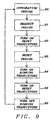
- Fig. 9 shows a block diagram showing the method of this invention.
- the imager accumulates charge in the pixels during an integration period when charge is stored by the photodiodes.
- the charge on the pixels is read out to a suitable location such as a register.
- the reset transistors are turned on and a reset period occurs when the initial charge on the photodiodes is restored.
- the binning transistors are turned on while the reset transistors are still on.
- the reset transistors are then turned off while the binning transistors are on. Having the binning transistors on when the reset transistors are turned off is key to the noise suppression of this method. Next, after the reset transistors have been turned off the binning transistors are turned off and the cycle can begin again with the next integration period.
- the binning gates have been shown in the context of a sensor array in which the photosensitive elements are formed from N - wells in a P - type substrate or P - type wells in an N - type substrate the binning gates could be implemented in arrays having conventional CMOS pixel structures.
Landscapes
- Engineering & Computer Science (AREA)
- Multimedia (AREA)
- Signal Processing (AREA)
- Physics & Mathematics (AREA)
- Electromagnetism (AREA)
- Solid State Image Pick-Up Elements (AREA)
- Transforming Light Signals Into Electric Signals (AREA)
Applications Claiming Priority (2)
| Application Number | Priority Date | Filing Date | Title |
|---|---|---|---|
| US339189 | 1982-01-15 | ||
| US10/339,189 US6878918B2 (en) | 2003-01-09 | 2003-01-09 | APS pixel with reset noise suppression and programmable binning capability |
Publications (2)
| Publication Number | Publication Date |
|---|---|
| EP1467410A2 true EP1467410A2 (de) | 2004-10-13 |
| EP1467410A3 EP1467410A3 (de) | 2006-04-12 |
Family
ID=32711058
Family Applications (1)
| Application Number | Title | Priority Date | Filing Date |
|---|---|---|---|
| EP04368002A Withdrawn EP1467410A3 (de) | 2003-01-09 | 2004-01-08 | Aktiver Pixelsensor mit Unterdrückung von Reset-Räuschen und programmierbarer Pixelzusammenfassungen |
Country Status (4)
| Country | Link |
|---|---|
| US (1) | US6878918B2 (de) |
| EP (1) | EP1467410A3 (de) |
| JP (1) | JP2004221585A (de) |
| KR (1) | KR20040064239A (de) |
Cited By (2)
| Publication number | Priority date | Publication date | Assignee | Title |
|---|---|---|---|---|
| WO2006130518A1 (en) | 2005-06-01 | 2006-12-07 | Eastman Kodak Company | Cmos image sensor pixel with selectable binning |
| WO2025235163A1 (en) * | 2024-05-08 | 2025-11-13 | Apple Inc. | Foveated sensor readout |
Families Citing this family (79)
| Publication number | Priority date | Publication date | Assignee | Title |
|---|---|---|---|---|
| DE19947536A1 (de) * | 1999-10-02 | 2001-04-05 | Philips Corp Intellectual Pty | Verfahren zum Auslesen der Sensorelemente eines Sensors sowie Sensor |
| US20070131992A1 (en) * | 2005-12-13 | 2007-06-14 | Dialog Semiconductor Gmbh | Multiple photosensor pixel image sensor |
| US20080136933A1 (en) * | 2006-12-11 | 2008-06-12 | Digital Imaging Systems Gmbh | Apparatus for controlling operation of a multiple photosensor pixel image sensor |
| US20080296639A1 (en) * | 2007-06-01 | 2008-12-04 | Dalsa Corporation | Semiconductor image sensor array device, apparatus comprising such a device and method for operating such a device |
| JP5499387B2 (ja) * | 2007-11-19 | 2014-05-21 | トリクセル | 画像放射線コリメータ構造を有する放射線検出器 |
| GB2457716A (en) | 2008-02-22 | 2009-08-26 | Cmosis Nv | Active pixel sensor (APS) array with selective passive pixel (charge binning) mode |
| US11792538B2 (en) | 2008-05-20 | 2023-10-17 | Adeia Imaging Llc | Capturing and processing of images including occlusions focused on an image sensor by a lens stack array |
| JP2011523538A (ja) | 2008-05-20 | 2011-08-11 | ペリカン イメージング コーポレイション | 異なる種類の撮像装置を有するモノリシックカメラアレイを用いた画像の撮像および処理 |
| US8866920B2 (en) | 2008-05-20 | 2014-10-21 | Pelican Imaging Corporation | Capturing and processing of images using monolithic camera array with heterogeneous imagers |
| US7777171B2 (en) * | 2008-08-26 | 2010-08-17 | Eastman Kodak Company | In-pixel summing of charge generated by two or more pixels having two reset transistors connected in series |
| US8130302B2 (en) * | 2008-11-07 | 2012-03-06 | Aptina Imaging Corporation | Methods and apparatus providing selective binning of pixel circuits |
| US8913166B2 (en) | 2009-01-21 | 2014-12-16 | Canon Kabushiki Kaisha | Solid-state imaging apparatus |
| WO2011053711A1 (en) * | 2009-10-30 | 2011-05-05 | Invisage Technologies, Inc. | Systems and methods for color binning |
| WO2011063347A2 (en) | 2009-11-20 | 2011-05-26 | Pelican Imaging Corporation | Capturing and processing of images using monolithic camera array with heterogeneous imagers |
| KR101829480B1 (ko) | 2010-04-09 | 2018-02-14 | 씬트-엑스 에이비 | x-선 센서 시스템 및 x-선 영상화 시스템 |
| WO2011143501A1 (en) | 2010-05-12 | 2011-11-17 | Pelican Imaging Corporation | Architectures for imager arrays and array cameras |
| KR101508283B1 (ko) * | 2010-06-01 | 2015-04-07 | 볼리 미디어 커뮤니케이션스 (센젠) 캄파니 리미티드 | 감광소자 및 그 리딩 방법, 리딩 회로 |
| US8878950B2 (en) | 2010-12-14 | 2014-11-04 | Pelican Imaging Corporation | Systems and methods for synthesizing high resolution images using super-resolution processes |
| EP2708019B1 (de) | 2011-05-11 | 2019-10-16 | FotoNation Limited | Systeme und verfahren zum senden und empfangen von arraykamera-bilddaten |
| FR2979485B1 (fr) * | 2011-08-26 | 2016-09-09 | E2V Semiconductors | Capteur d'image a regroupement de pixels |
| WO2013043761A1 (en) | 2011-09-19 | 2013-03-28 | Pelican Imaging Corporation | Determining depth from multiple views of a scene that include aliasing using hypothesized fusion |
| US9129183B2 (en) | 2011-09-28 | 2015-09-08 | Pelican Imaging Corporation | Systems and methods for encoding light field image files |
| US9412206B2 (en) | 2012-02-21 | 2016-08-09 | Pelican Imaging Corporation | Systems and methods for the manipulation of captured light field image data |
| US9210392B2 (en) | 2012-05-01 | 2015-12-08 | Pelican Imaging Coporation | Camera modules patterned with pi filter groups |
| EP2873028A4 (de) | 2012-06-28 | 2016-05-25 | Pelican Imaging Corp | Systeme und verfahren zur erkennung defekter kamera-arrays, optischer arrays und sensoren |
| US20140002674A1 (en) | 2012-06-30 | 2014-01-02 | Pelican Imaging Corporation | Systems and Methods for Manufacturing Camera Modules Using Active Alignment of Lens Stack Arrays and Sensors |
| KR102111181B1 (ko) | 2012-08-21 | 2020-05-15 | 포토내이션 리미티드 | 어레이 카메라를 사용하여 포착된 영상에서의 시차 검출 및 보정을 위한 시스템 및 방법 |
| WO2014032020A2 (en) | 2012-08-23 | 2014-02-27 | Pelican Imaging Corporation | Feature based high resolution motion estimation from low resolution images captured using an array source |
| WO2014043641A1 (en) | 2012-09-14 | 2014-03-20 | Pelican Imaging Corporation | Systems and methods for correcting user identified artifacts in light field images |
| EP2901671A4 (de) | 2012-09-28 | 2016-08-24 | Pelican Imaging Corp | Erzeugung von bildern aus lichtfeldern mithilfe virtueller blickpunkte |
| WO2014078443A1 (en) | 2012-11-13 | 2014-05-22 | Pelican Imaging Corporation | Systems and methods for array camera focal plane control |
| US9462164B2 (en) | 2013-02-21 | 2016-10-04 | Pelican Imaging Corporation | Systems and methods for generating compressed light field representation data using captured light fields, array geometry, and parallax information |
| WO2014133974A1 (en) | 2013-02-24 | 2014-09-04 | Pelican Imaging Corporation | Thin form computational and modular array cameras |
| WO2014138697A1 (en) | 2013-03-08 | 2014-09-12 | Pelican Imaging Corporation | Systems and methods for high dynamic range imaging using array cameras |
| US8866912B2 (en) | 2013-03-10 | 2014-10-21 | Pelican Imaging Corporation | System and methods for calibration of an array camera using a single captured image |
| US9521416B1 (en) | 2013-03-11 | 2016-12-13 | Kip Peli P1 Lp | Systems and methods for image data compression |
| US9106784B2 (en) | 2013-03-13 | 2015-08-11 | Pelican Imaging Corporation | Systems and methods for controlling aliasing in images captured by an array camera for use in super-resolution processing |
| WO2014164909A1 (en) | 2013-03-13 | 2014-10-09 | Pelican Imaging Corporation | Array camera architecture implementing quantum film sensors |
| US9124831B2 (en) | 2013-03-13 | 2015-09-01 | Pelican Imaging Corporation | System and methods for calibration of an array camera |
| WO2014165244A1 (en) | 2013-03-13 | 2014-10-09 | Pelican Imaging Corporation | Systems and methods for synthesizing images from image data captured by an array camera using restricted depth of field depth maps in which depth estimation precision varies |
| US9100586B2 (en) | 2013-03-14 | 2015-08-04 | Pelican Imaging Corporation | Systems and methods for photometric normalization in array cameras |
| US9578259B2 (en) | 2013-03-14 | 2017-02-21 | Fotonation Cayman Limited | Systems and methods for reducing motion blur in images or video in ultra low light with array cameras |
| JP2016524125A (ja) | 2013-03-15 | 2016-08-12 | ペリカン イメージング コーポレイション | カメラアレイを用いた立体撮像のためのシステムおよび方法 |
| US9445003B1 (en) | 2013-03-15 | 2016-09-13 | Pelican Imaging Corporation | Systems and methods for synthesizing high resolution images using image deconvolution based on motion and depth information |
| US10122993B2 (en) | 2013-03-15 | 2018-11-06 | Fotonation Limited | Autofocus system for a conventional camera that uses depth information from an array camera |
| WO2014150856A1 (en) | 2013-03-15 | 2014-09-25 | Pelican Imaging Corporation | Array camera implementing quantum dot color filters |
| US9497429B2 (en) | 2013-03-15 | 2016-11-15 | Pelican Imaging Corporation | Extended color processing on pelican array cameras |
| KR102087225B1 (ko) * | 2013-05-30 | 2020-03-11 | 에스케이하이닉스 주식회사 | 이미지 센싱 장치 |
| WO2015048694A2 (en) | 2013-09-27 | 2015-04-02 | Pelican Imaging Corporation | Systems and methods for depth-assisted perspective distortion correction |
| US9426343B2 (en) | 2013-11-07 | 2016-08-23 | Pelican Imaging Corporation | Array cameras incorporating independently aligned lens stacks |
| US10119808B2 (en) | 2013-11-18 | 2018-11-06 | Fotonation Limited | Systems and methods for estimating depth from projected texture using camera arrays |
| WO2015081279A1 (en) | 2013-11-26 | 2015-06-04 | Pelican Imaging Corporation | Array camera configurations incorporating multiple constituent array cameras |
| US10089740B2 (en) | 2014-03-07 | 2018-10-02 | Fotonation Limited | System and methods for depth regularization and semiautomatic interactive matting using RGB-D images |
| US9674470B2 (en) * | 2014-04-11 | 2017-06-06 | Semiconductor Energy Laboratory Co., Ltd. | Semiconductor device, method for driving semiconductor device, and method for driving electronic device |
| US9521319B2 (en) | 2014-06-18 | 2016-12-13 | Pelican Imaging Corporation | Array cameras and array camera modules including spectral filters disposed outside of a constituent image sensor |
| EP3467776A1 (de) | 2014-09-29 | 2019-04-10 | Fotonation Cayman Limited | Systeme und verfahren zur dynamischen kalibrierung von array-kameras |
| FR3030884B1 (fr) * | 2014-12-19 | 2016-12-30 | Stmicroelectronics (Grenoble 2) Sas | Structure de pixel a multiples photosites |
| US9942474B2 (en) | 2015-04-17 | 2018-04-10 | Fotonation Cayman Limited | Systems and methods for performing high speed video capture and depth estimation using array cameras |
| FR3043495A1 (fr) * | 2015-11-09 | 2017-05-12 | St Microelectronics Crolles 2 Sas | Capteur d'images a obturation globale |
| US10313610B2 (en) | 2016-04-14 | 2019-06-04 | Qualcomm Incorporated | Image sensors with dynamic pixel binning |
| US10313609B2 (en) | 2016-04-14 | 2019-06-04 | Qualcomm Incorporated | Image sensors having pixel-binning with configurable shared floating diffusion |
| US10482618B2 (en) | 2017-08-21 | 2019-11-19 | Fotonation Limited | Systems and methods for hybrid depth regularization |
| US11445129B2 (en) * | 2018-03-09 | 2022-09-13 | Imasenic Advanced Imaging, S.L. | Binning pixels |
| KR102646521B1 (ko) | 2019-09-17 | 2024-03-21 | 인트린식 이노베이션 엘엘씨 | 편광 큐를 이용한 표면 모델링 시스템 및 방법 |
| MX2022004163A (es) | 2019-10-07 | 2022-07-19 | Boston Polarimetrics Inc | Sistemas y metodos para la deteccion de estandares de superficie con polarizacion. |
| DE112020005932T5 (de) | 2019-11-30 | 2023-01-05 | Boston Polarimetrics, Inc. | Systeme und verfahren zur segmentierung von transparenten objekten mittels polarisationsmerkmalen |
| EP4081933B1 (de) | 2020-01-29 | 2026-03-04 | Intrinsic Innovation LLC | Systeme und verfahren zur charakterisierung von objektposenerfassung und messsysteme |
| EP4085424A4 (de) | 2020-01-30 | 2024-03-27 | Intrinsic Innovation LLC | Systeme und verfahren zum synthetisieren von daten für das trainieren von statistischen modellen auf verschiedenen bildgebenden modalitäten, einschliesslich polarisierter bilder |
| US11953700B2 (en) | 2020-05-27 | 2024-04-09 | Intrinsic Innovation Llc | Multi-aperture polarization optical systems using beam splitters |
| US12020455B2 (en) | 2021-03-10 | 2024-06-25 | Intrinsic Innovation Llc | Systems and methods for high dynamic range image reconstruction |
| US12069227B2 (en) | 2021-03-10 | 2024-08-20 | Intrinsic Innovation Llc | Multi-modal and multi-spectral stereo camera arrays |
| US11290658B1 (en) | 2021-04-15 | 2022-03-29 | Boston Polarimetrics, Inc. | Systems and methods for camera exposure control |
| US11954886B2 (en) | 2021-04-15 | 2024-04-09 | Intrinsic Innovation Llc | Systems and methods for six-degree of freedom pose estimation of deformable objects |
| US12067746B2 (en) | 2021-05-07 | 2024-08-20 | Intrinsic Innovation Llc | Systems and methods for using computer vision to pick up small objects |
| US12175741B2 (en) | 2021-06-22 | 2024-12-24 | Intrinsic Innovation Llc | Systems and methods for a vision guided end effector |
| US12340538B2 (en) | 2021-06-25 | 2025-06-24 | Intrinsic Innovation Llc | Systems and methods for generating and using visual datasets for training computer vision models |
| US12172310B2 (en) | 2021-06-29 | 2024-12-24 | Intrinsic Innovation Llc | Systems and methods for picking objects using 3-D geometry and segmentation |
| US11689813B2 (en) | 2021-07-01 | 2023-06-27 | Intrinsic Innovation Llc | Systems and methods for high dynamic range imaging using crossed polarizers |
| US12293535B2 (en) | 2021-08-03 | 2025-05-06 | Intrinsic Innovation Llc | Systems and methods for training pose estimators in computer vision |
Family Cites Families (10)
| Publication number | Priority date | Publication date | Assignee | Title |
|---|---|---|---|---|
| JPS5941351B2 (ja) * | 1976-09-13 | 1984-10-06 | 株式会社日立製作所 | カラ−用固体撮像素子 |
| US5134488A (en) | 1990-12-28 | 1992-07-28 | David Sarnoff Research Center, Inc. | X-Y addressable imager with variable integration |
| US5134489A (en) | 1990-12-28 | 1992-07-28 | David Sarnoff Research Center, Inc. | X-Y addressable solid state imager for low noise operation |
| FI97665C (fi) | 1995-11-21 | 1997-01-27 | Planmed Oy | Menetelmät ja laitteet kohteen kuvantamisessa |
| US5970115A (en) | 1996-11-29 | 1999-10-19 | Varian Medical Systems, Inc. | Multiple mode digital X-ray imaging system |
| FR2794287B1 (fr) * | 1999-05-25 | 2003-06-06 | Commissariat Energie Atomique | Detecteur a semi-conducteur pour la detection de rayonnements ionisants |
| EP1102323B1 (de) * | 1999-11-19 | 2012-08-15 | CSEM Centre Suisse d'Electronique et de Microtechnique SA - Recherche et Développement | Verfahren zum Detektieren von elektromagnetischer Strahlung mittels eines optoelektronischen Sensors |
| US6365926B1 (en) * | 2000-09-20 | 2002-04-02 | Eastman Kodak Company | CMOS active pixel with scavenging diode |
| US6759641B1 (en) * | 2000-09-27 | 2004-07-06 | Rockwell Scientific Licensing, Llc | Imager with adjustable resolution |
| US6756616B2 (en) * | 2001-08-30 | 2004-06-29 | Micron Technology, Inc. | CMOS imager and method of formation |
-
2003
- 2003-01-09 US US10/339,189 patent/US6878918B2/en not_active Expired - Lifetime
-
2004
- 2004-01-08 EP EP04368002A patent/EP1467410A3/de not_active Withdrawn
- 2004-01-09 JP JP2004003819A patent/JP2004221585A/ja active Pending
- 2004-01-09 KR KR1020040001696A patent/KR20040064239A/ko not_active Withdrawn
Cited By (3)
| Publication number | Priority date | Publication date | Assignee | Title |
|---|---|---|---|---|
| WO2006130518A1 (en) | 2005-06-01 | 2006-12-07 | Eastman Kodak Company | Cmos image sensor pixel with selectable binning |
| US7705900B2 (en) | 2005-06-01 | 2010-04-27 | Eastman Kodak Company | CMOS image sensor pixel with selectable binning and conversion gain |
| WO2025235163A1 (en) * | 2024-05-08 | 2025-11-13 | Apple Inc. | Foveated sensor readout |
Also Published As
| Publication number | Publication date |
|---|---|
| KR20040064239A (ko) | 2004-07-16 |
| US6878918B2 (en) | 2005-04-12 |
| EP1467410A3 (de) | 2006-04-12 |
| US20040135063A1 (en) | 2004-07-15 |
| JP2004221585A (ja) | 2004-08-05 |
Similar Documents
| Publication | Publication Date | Title |
|---|---|---|
| US6878918B2 (en) | APS pixel with reset noise suppression and programmable binning capability | |
| US6603513B1 (en) | Using a single control line to provide select and reset signals to image sensors in two rows of a digital imaging device | |
| US9543350B2 (en) | Solid-state imaging device and camera including discrete trench isolation structure | |
| US8004026B2 (en) | Solid-state imaging device | |
| JP3412390B2 (ja) | 光電変換装置 | |
| US20060208163A1 (en) | CMOS image sensor using shared transistors between pixels having mirror symmetry | |
| US7834304B2 (en) | Imaging device | |
| US5430481A (en) | Multimode frame transfer image sensor | |
| CN102005461A (zh) | 固体摄像器件、固体摄像器件制造方法和电子装置 | |
| KR900005875B1 (ko) | 고체 촬성 소자 | |
| US6882022B2 (en) | Dual gate BCMD pixel suitable for high performance CMOS image sensor arrays | |
| KR20040064237A (ko) | 이중 게이트 pmos를 구비한 cmos 화소 | |
| EP0734069B1 (de) | Schalttransistor für eine Festkörperbildaufnahmevorrichtung | |
| EP0216426A1 (de) | Bildaufnahmeanordnungen mit photovoltaischen Detektorelementen | |
| US7471326B2 (en) | Scanning switch transistor for solid-state imaging device | |
| KR100769563B1 (ko) | 누설 전류를 감소시킨 이미지 센서 | |
| JPS62206878A (ja) | 固体撮像素子 | |
| JP2003324191A (ja) | 光電変換装置及び撮像装置 | |
| KR830000197B1 (ko) | 고체 촬상장치 | |
| JPH05152552A (ja) | 固体撮像装置 | |
| JPH04343473A (ja) | Ccd転送回路とccd固体撮像素子 | |
| JPH0773345B2 (ja) | 接合電界効果型固体撮像装置とその駆動方法 |
Legal Events
| Date | Code | Title | Description |
|---|---|---|---|
| PUAI | Public reference made under article 153(3) epc to a published international application that has entered the european phase |
Free format text: ORIGINAL CODE: 0009012 |
|
| AK | Designated contracting states |
Kind code of ref document: A2 Designated state(s): AT BE BG CH CY CZ DE DK EE ES FI FR GB GR HU IE IT LI LU MC NL PT RO SE SI SK TR |
|
| AX | Request for extension of the european patent |
Extension state: AL LT LV MK |
|
| PUAL | Search report despatched |
Free format text: ORIGINAL CODE: 0009013 |
|
| AK | Designated contracting states |
Kind code of ref document: A3 Designated state(s): AT BE BG CH CY CZ DE DK EE ES FI FR GB GR HU IE IT LI LU MC NL PT RO SE SI SK TR |
|
| AX | Request for extension of the european patent |
Extension state: AL LT LV MK |
|
| AKX | Designation fees paid | ||
| REG | Reference to a national code |
Ref country code: DE Ref legal event code: 8566 |
|
| STAA | Information on the status of an ep patent application or granted ep patent |
Free format text: STATUS: THE APPLICATION IS DEEMED TO BE WITHDRAWN |
|
| 18D | Application deemed to be withdrawn |
Effective date: 20061013 |