EP1469446A2 - Procédé de commande d'un panneau d'affichage - Google Patents
Procédé de commande d'un panneau d'affichage Download PDFInfo
- Publication number
- EP1469446A2 EP1469446A2 EP04251875A EP04251875A EP1469446A2 EP 1469446 A2 EP1469446 A2 EP 1469446A2 EP 04251875 A EP04251875 A EP 04251875A EP 04251875 A EP04251875 A EP 04251875A EP 1469446 A2 EP1469446 A2 EP 1469446A2
- Authority
- EP
- European Patent Office
- Prior art keywords
- electrode
- pulse
- sustain
- display panel
- row
- Prior art date
- Legal status (The legal status is an assumption and is not a legal conclusion. Google has not performed a legal analysis and makes no representation as to the accuracy of the status listed.)
- Withdrawn
Links
Images



Classifications
-
- G—PHYSICS
- G09—EDUCATION; CRYPTOGRAPHY; DISPLAY; ADVERTISING; SEALS
- G09G—ARRANGEMENTS OR CIRCUITS FOR CONTROL OF INDICATING DEVICES USING STATIC MEANS TO PRESENT VARIABLE INFORMATION
- G09G3/00—Control arrangements or circuits, of interest only in connection with visual indicators other than cathode-ray tubes
- G09G3/20—Control arrangements or circuits, of interest only in connection with visual indicators other than cathode-ray tubes for presentation of an assembly of a number of characters, e.g. a page, by composing the assembly by combination of individual elements arranged in a matrix no fixed position being assigned to or needed to be assigned to the individual characters or partial characters
- G09G3/22—Control arrangements or circuits, of interest only in connection with visual indicators other than cathode-ray tubes for presentation of an assembly of a number of characters, e.g. a page, by composing the assembly by combination of individual elements arranged in a matrix no fixed position being assigned to or needed to be assigned to the individual characters or partial characters using controlled light sources
- G09G3/28—Control arrangements or circuits, of interest only in connection with visual indicators other than cathode-ray tubes for presentation of an assembly of a number of characters, e.g. a page, by composing the assembly by combination of individual elements arranged in a matrix no fixed position being assigned to or needed to be assigned to the individual characters or partial characters using controlled light sources using luminous gas-discharge panels, e.g. plasma panels
- G09G3/288—Control arrangements or circuits, of interest only in connection with visual indicators other than cathode-ray tubes for presentation of an assembly of a number of characters, e.g. a page, by composing the assembly by combination of individual elements arranged in a matrix no fixed position being assigned to or needed to be assigned to the individual characters or partial characters using controlled light sources using luminous gas-discharge panels, e.g. plasma panels using AC panels
- G09G3/296—Driving circuits for producing the waveforms applied to the driving electrodes
- G09G3/2965—Driving circuits for producing the waveforms applied to the driving electrodes using inductors for energy recovery
-
- G—PHYSICS
- G09—EDUCATION; CRYPTOGRAPHY; DISPLAY; ADVERTISING; SEALS
- G09G—ARRANGEMENTS OR CIRCUITS FOR CONTROL OF INDICATING DEVICES USING STATIC MEANS TO PRESENT VARIABLE INFORMATION
- G09G3/00—Control arrangements or circuits, of interest only in connection with visual indicators other than cathode-ray tubes
- G09G3/20—Control arrangements or circuits, of interest only in connection with visual indicators other than cathode-ray tubes for presentation of an assembly of a number of characters, e.g. a page, by composing the assembly by combination of individual elements arranged in a matrix no fixed position being assigned to or needed to be assigned to the individual characters or partial characters
- G09G3/22—Control arrangements or circuits, of interest only in connection with visual indicators other than cathode-ray tubes for presentation of an assembly of a number of characters, e.g. a page, by composing the assembly by combination of individual elements arranged in a matrix no fixed position being assigned to or needed to be assigned to the individual characters or partial characters using controlled light sources
- G09G3/28—Control arrangements or circuits, of interest only in connection with visual indicators other than cathode-ray tubes for presentation of an assembly of a number of characters, e.g. a page, by composing the assembly by combination of individual elements arranged in a matrix no fixed position being assigned to or needed to be assigned to the individual characters or partial characters using controlled light sources using luminous gas-discharge panels, e.g. plasma panels
- G09G3/288—Control arrangements or circuits, of interest only in connection with visual indicators other than cathode-ray tubes for presentation of an assembly of a number of characters, e.g. a page, by composing the assembly by combination of individual elements arranged in a matrix no fixed position being assigned to or needed to be assigned to the individual characters or partial characters using controlled light sources using luminous gas-discharge panels, e.g. plasma panels using AC panels
- G09G3/291—Control arrangements or circuits, of interest only in connection with visual indicators other than cathode-ray tubes for presentation of an assembly of a number of characters, e.g. a page, by composing the assembly by combination of individual elements arranged in a matrix no fixed position being assigned to or needed to be assigned to the individual characters or partial characters using controlled light sources using luminous gas-discharge panels, e.g. plasma panels using AC panels controlling the gas discharge to control a cell condition, e.g. by means of specific pulse shapes
- G09G3/294—Control arrangements or circuits, of interest only in connection with visual indicators other than cathode-ray tubes for presentation of an assembly of a number of characters, e.g. a page, by composing the assembly by combination of individual elements arranged in a matrix no fixed position being assigned to or needed to be assigned to the individual characters or partial characters using controlled light sources using luminous gas-discharge panels, e.g. plasma panels using AC panels controlling the gas discharge to control a cell condition, e.g. by means of specific pulse shapes for lighting or sustain discharge
-
- G—PHYSICS
- G09—EDUCATION; CRYPTOGRAPHY; DISPLAY; ADVERTISING; SEALS
- G09G—ARRANGEMENTS OR CIRCUITS FOR CONTROL OF INDICATING DEVICES USING STATIC MEANS TO PRESENT VARIABLE INFORMATION
- G09G3/00—Control arrangements or circuits, of interest only in connection with visual indicators other than cathode-ray tubes
- G09G3/20—Control arrangements or circuits, of interest only in connection with visual indicators other than cathode-ray tubes for presentation of an assembly of a number of characters, e.g. a page, by composing the assembly by combination of individual elements arranged in a matrix no fixed position being assigned to or needed to be assigned to the individual characters or partial characters
- G09G3/22—Control arrangements or circuits, of interest only in connection with visual indicators other than cathode-ray tubes for presentation of an assembly of a number of characters, e.g. a page, by composing the assembly by combination of individual elements arranged in a matrix no fixed position being assigned to or needed to be assigned to the individual characters or partial characters using controlled light sources
- G09G3/28—Control arrangements or circuits, of interest only in connection with visual indicators other than cathode-ray tubes for presentation of an assembly of a number of characters, e.g. a page, by composing the assembly by combination of individual elements arranged in a matrix no fixed position being assigned to or needed to be assigned to the individual characters or partial characters using controlled light sources using luminous gas-discharge panels, e.g. plasma panels
- G09G3/288—Control arrangements or circuits, of interest only in connection with visual indicators other than cathode-ray tubes for presentation of an assembly of a number of characters, e.g. a page, by composing the assembly by combination of individual elements arranged in a matrix no fixed position being assigned to or needed to be assigned to the individual characters or partial characters using controlled light sources using luminous gas-discharge panels, e.g. plasma panels using AC panels
- G09G3/296—Driving circuits for producing the waveforms applied to the driving electrodes
-
- G—PHYSICS
- G09—EDUCATION; CRYPTOGRAPHY; DISPLAY; ADVERTISING; SEALS
- G09G—ARRANGEMENTS OR CIRCUITS FOR CONTROL OF INDICATING DEVICES USING STATIC MEANS TO PRESENT VARIABLE INFORMATION
- G09G2310/00—Command of the display device
- G09G2310/06—Details of flat display driving waveforms
- G09G2310/066—Waveforms comprising a gently increasing or decreasing portion, e.g. ramp
-
- G—PHYSICS
- G09—EDUCATION; CRYPTOGRAPHY; DISPLAY; ADVERTISING; SEALS
- G09G—ARRANGEMENTS OR CIRCUITS FOR CONTROL OF INDICATING DEVICES USING STATIC MEANS TO PRESENT VARIABLE INFORMATION
- G09G2330/00—Aspects of power supply; Aspects of display protection and defect management
- G09G2330/02—Details of power systems and of start or stop of display operation
- G09G2330/021—Power management, e.g. power saving
- G09G2330/023—Power management, e.g. power saving using energy recovery or conservation
-
- G—PHYSICS
- G09—EDUCATION; CRYPTOGRAPHY; DISPLAY; ADVERTISING; SEALS
- G09G—ARRANGEMENTS OR CIRCUITS FOR CONTROL OF INDICATING DEVICES USING STATIC MEANS TO PRESENT VARIABLE INFORMATION
- G09G2330/00—Aspects of power supply; Aspects of display protection and defect management
- G09G2330/04—Display protection
- G09G2330/045—Protection against panel overheating
Definitions
- the present invention relates to display panel driving methods for driving display panels such as plasma display panels (hereafter, “PDP”) and electroluminescence (hereafter, “EL”) panels.
- display panels such as plasma display panels (hereafter, “PDP”) and electroluminescence (hereafter, “EL”) panels.
- PDP plasma display panels
- EL electroluminescence
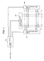
- Patent Document 1 An overall configuration of the drive circuit in the PDP display device disclosed in Patent Document 1 is shown in the block diagram of FIG. 1.
- a display panel PDP 10 has row electrodes X 1 to X n and row electrodes Y 1 to Y n , which are formed such that each pair of a row electrode X and a row electrode Y constitutes a row electrode pair corresponding to a row (first row to n-th row) of one screen. Furthermore, in the PDP 10, column electrodes Z 1 to Z m are formed perpendicular to the row electrodes, sandwiching a dielectric layer and a discharge space layer, which are not shown in the drawing, and correspond to columns (first column to m-th column) of one screen. It should be noted that a single discharge cell C ( i, j ) is formed at the intersecting portion of each single pair of row electrodes (X i , Y i ) and single column electrode Z j .
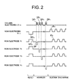
- a row electrode drive circuit 30 produces a positive reset pulse RP y like that shown in FIG. 2, which is simultaneously applied to each of the row electrodes Y 1 to Y n .
- a row electrode drive circuit 40 produces a negative reset pulse RP x , which is simultaneously applied to all the row electrodes X 1 to X n .
- a discharge is induced in all the discharge cells of the PDP 10, generating charged particles. Subsequent to the completion of this discharge, a predetermined wall charge is formed uniformly in the dielectric layer of all the discharge cells. This processing step is referred to as a reset step.
- a column electrode drive circuit 20 After the completion of the reset step, a column electrode drive circuit 20 produces pixel data pulses DP 1 to DP n corresponding to pixel data that corresponds to the first to n-th rows of the screen. The pixel data pulses are then applied successively to the column electrodes Z 1 to Z m as shown in Fig. 2. Meanwhile, the row electrode drive circuit 30 produces negative scan pulses SP corresponding to the timing of the application of the pixel data pulses DP 1 to DP n . Then, as shown in Fig. 2, the negative scan pulses are applied successively to the row electrodes Y 1 to Y n .
- the row electrode drive circuit 30 continuously applies positive sustain pulses IP Y to the row electrodes Y 1 to Y n as shown in FIG. 2.
- the row electrode drive circuit 40 continuously applies positive sustain pulses IP X to the row electrodes X 1 to X n with a timing that is offset against the timing of the sustain pulses IP Y .
- discharge light emissions are repeated by the light-emitting discharge cells in which the above-mentioned wall charge remains as it is, thus maintaining a light-emitting state.
- This processing step is referred to as a sustain step.
- a drive control circuit 50 produces various switching signals based on the timing of the supplied video signal in order for the various drive pulses shown in FIG. 2 to be produced. These switching signals are then supplied to the above-mentioned column electrode drive circuit 20, and the row electrode drive circuits 30 and 40. That is, the column electrode drive circuit 20 and the row electrode drive circuits 30 and 40 produce the drive pulses shown in FIG. 2 in response to the switching signals supplied from the drive control circuit 50.
- pulse generating circuits which generate the various drive pulses such as the reset pulse RP Y and the sustain pulses IP X and IP Y , are provided for each row and column electrode inside the above-mentioned electrode drive circuits. It should be noted that all of these pulse generating circuits use the charging and discharging of capacitors in LC resonance circuits made of an inductor L and a capacitor C to generate the various drive pulses.
- the resonance circuits are formed combining inductors, which are inductive elements, and capacitors for power collection exploiting the fact that the discharge cells C ( i, j ) of the PDP 10 are capacitive loads.
- a desired driving pulse is then generated by exciting the resonance circuits with a predetermined timing by opening and closing switching elements such as FETs in response to switching signals supplied from the drive control circuit 50.
- the prior art described above aim to improve power dissipation when driving a display panel by using resonance circuits for the circuits that drive the discharge cells, which constitute capacitive loads.
- a comparatively high voltage of around several tens to one hundred and several tens of volts is used when exciting discharge cells with resonance circuits. For this reason, the power dissipation is still large when driving a display panel and there is a need for improved reductions in reactive power.
- the present invention has been made to solve such a problem as described above.
- Examples of the objects to be attained by the present invention include, for example, providing a display panel driving method that can reduce power consumption when exciting discharge cells.
- a display panel driving method for driving a display panel including a plurality of row electrode pairs, a plurality of column electrodes arranged intersecting the plurality of row electrode pairs, and capacitive light-emitting elements arranged at an intersecting point of the row electrode pairs and the column electrodes, and in which driving is performed by repeating a driving step that comprises an addressing step and a sustain step, wherein during the period of the sustain step, an output terminal of a column electrode drive circuit connected to one of the row electrodes is maintained in a high impedance state, and bipolar pulse signals with different phases are supplied to each of a first row electrode and a second row electrode that configures each of the row electrode pairs.
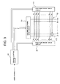
- FIG. 3 is a block diagram showing a configuration of a display panel driving device that executes a display panel driving method according to the present invention.
- a display panel PDP 10 is provided with row electrodes X 1 to X n and row electrodes Y 1 to Y n , which are formed such that each pair of a row electrode X and a row electrode Y constitutes a row electrode pair corresponding to a row (first row to n-th row) of one screen. Furthermore, in the PDP 10, column electrodes Z 1 to Z m are formed perpendicular to the row electrodes, sandwiching a dielectric layer and a discharge space layer, which are not shown in the drawing, and correspond to columns (first column to m-th column) of one screen. It should be noted that a single discharge cell C (i, j) is formed at the intersecting portion of each single pair of row electrodes (X i , Y i ) and single column electrode Z j .
- a row electrode drive circuit 31 produces various drive pulses, such as the above-mentioned reset pulses and sustain pulses, and applies these pulses to the row electrodes Y 1 to Y n with a predetermined timing.
- a row electrode drive circuit 41 also produces various drive pulses and applies these pulses to the row electrodes X 1 to X n with a predetermined timing.
- a column electrode drive circuit 21 produces pixel data pulses corresponding to pixel data that corresponds to the first to n-th display lines, and these pulses are applied successively to the column electrodes Z 1 to Z m .
- pulse generating circuits which generate the various above-mentioned drive pulses, are provided for each row and column electrode inside the row electrode drive circuits 31 and 41, and the column electrode drive circuit 21.
- a drive control circuit 51 produces various switching signals based on the supplied video signal in order for the various, above-mentioned drive pulses to be produced. These switching signals are then supplied to the pulse generating circuits that are arranged inside the column electrode drive circuit 21, and the row electrode drive circuits 31 and 41.
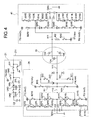
- the circuit shown in FIG. 4 is only an exemplary embodiment of a circuit with which a display panel driving method according to the present invention can be executed, and that the present invention is in no way limited to the circuit configuration of this embodiment.
- the circuit shown in FIG. 4 demonstrates a configuration of a single discharge cell of the PDP 10, that is, a configuration of a pulse generating circuit involving a single pair of row electrodes and a single column electrode. Accordingly, the pulse generating circuit shown in FIG. 4 is arranged inside each of the row electrode drive circuits 31 and 41 and the column electrode drive circuit 21 for each of the first to n-th row of display lines and for each of the first to m-th columns of one screen.
- the ground terminal (O V) of an unshown DC power source which produces DC voltages +Vs/2 and -Vs/2, is connected to a ground potential G (0 V), which is the ground potential of the PDP 10.
- a positive terminal (+Vs/2) of the DC power source is connected to a power source terminal T1
- a negative terminal (-Vs/2) is connected to a power source terminal T2.
- a switch B2YS is connected to the power source terminal T1
- the other terminal of the switch B2YS is connected to the anode of a diode G2YD, one terminal each of a serial branch U2Y and a serial branch D2Y, and a connecting line Y12.
- serial branch U2Y refers to a serial circuit made of an inductor U2YL, a diode U2YD, and a switch U2YS.
- serial branch D2Y refers to a serial circuit made of an inductor D2YL, a diode D2YD, and a switch D2YS.
- both of the other terminals of the serial branch U2Y and the serial branch D2Y are connected to one terminal of a capacitor C2, while the other terminal of the capacitor C2 is connected to the ground G (0 V).
- the portion made of the serial branch U2Y, the serial branch D2Y, and the capacitor C2 makes up a single resonance circuit in the pulse generating circuit contained in the row electrode drive circuit 31.
- the cathode of a diode G2YD is connected to one terminal of a switch G2YS, while the other terminal of the switch G2YS is connected to the anode of a diode B1YD, the other terminal of the above-mentioned capacitor C2, and the ground G (0V).
- serial branch U1Y refers to a serial circuit made of an inductor U1YL, a diode U1YD, and a switch U1YS.
- serial branch D1Y refers to a serial circuit made of an inductor D1YL, a diode D1YD, and a switch D1YS.
- both of the other terminals of the serial branch U1Y and the serial branch D1Y are connected to one terminal of a capacitor C1, while the other terminal of the capacitor C1 is connected to the ground G (0 V).
- the portion made of the serial branch U1Y, the serial branch D1Y, and the capacitor C1 makes up another single resonance circuit in the pulse generating circuit contained in the row electrode drive circuit 31.
- the other terminal of the switch G1YS is connected to the power source terminal T2 (-Vs/2).
- the connecting line Y12 is connected to one terminal of a resistor R1, one terminal of a switch VofS, the cathode of a bias power source Vh, one terminal of a switch S21, and the anode of a diode D21.
- the other terminal of the resistor R1 is connected via a switch RYS to a power source terminal T3 (+Vry), while the other terminal of the switch VofS is connected to a power source terminal T4 (-Vof).
- the anode of the power source Vh is connected to one terminal of a switch S22 and the cathode of a diode D22.
- the other terminals of the switch 21 and the switch 22, as well as the cathode of the diode D21 and the anode of the diode D22, are connected to a connecting line Y11.
- the circuit arranged between the connecting line Y12 and the connecting line Y11 is the portion that generates the reset pulses and the scanning pulses in the reset step and the addressing step.
- the connecting line Y11 is an output terminal for the pulse signal that leads to the Y row electrode of the PDP 10, and is therefore connected to the capacitance component of the discharge cell C ( i,j ) in the PDP 10.
- the DC voltage +Vs/2 from the unshown power source circuit is connected to a power source terminal T5, and the DC voltage -Vs/2 is connected to a power source terminal T6.
- one terminal of a switch B2XS is connected to the power source terminal T5, and the other terminal of the switch B2XS is connected to an anode of a diode G2XD, one terminal each of a serial branch U2X and a serial branch D2X, and the connecting line Y11.
- serial branch U2X refers to a serial circuit made of an inductor U2XL, a diode U2XD, and a switch U2XS.
- serial branch D2X refers to a serial circuit made of an inductor D2XL, a diode D2XD, and a switch D2XS.
- Both of the other terminals of the serial branch U2X and the serial branch D2X are connected to one terminal of a capacitor C4, while the other terminal of the capacitor C4 is connected to the ground G (0 V).
- the portion made of the serial branch U2X, the serial branch D2X, and the capacitor C4 makes up a single resonance circuit in the pulse generating circuit contained in the row electrode drive circuit 41.
- the cathode of a diode G2XD is connected to one terminal of a switch G2XS, while the other terminal of the switch G2XS is connected to the anode of a diode B1XD, the other terminal of the above-mentioned capacitor C4, and the ground G (0 V).
- serial branch U1X refers to a serial circuit made of an inductor U1XL, a diode U1XD, and a switch U1XS.
- serial branch D1X refers to a serial circuit made of an inductor D1XL, a diode D1XD, and a switch D1XS.
- Both of the other terminals of the serial branch U1X and the serial branch D1X are connected to one terminal of a capacitor C3, while the other terminal of the capacitor C3 is connected to the ground G (0 V).
- the portion made of the serial branch U1X, the serial branch D1X, and the capacitor C3 makes up another single resonance circuit in the pulse generating circuit contained in the row electrode drive circuit 41.
- the other terminal of the switch G1XS is connected to the power source terminal T6 (-Vs/2).
- the connecting line X11 is connected to one terminal of a resistor R2, and the other terminal of the resistor R2 is connected via a switch RXS to a power source terminal T7 (+Vrx).
- the connecting line Y11 is an output terminal for the pulse signal that leads to the X row electrode of the PDP 10, and is therefore connected to the capacitance component of the discharge cell C ( i, j ) in the PDP 10.
- a DC voltage +Va from an unshown power source circuit is connected to a power source terminal T8, and is also connected to one terminal of a switch BAS.
- serial branch UA refers to a serial circuit made of an inductor UAL, a diode UAD, and a switch UAS.
- serial branch DA refers to a serial circuit made of an inductor DAL, a diode DAD, and a switch DAS.
- both of the other terminals of the serial branch UA and the serial branch DA are connected to one terminal of a capacitor C5, while the other terminal of the capacitor C5 is connected to the ground G (0 V).
- the portion made of the serial branch UA, the serial branch DA, and the capacitor C5 makes up a single resonance circuit in the pulse generating circuit contained in the column electrode drive circuit 21.
- the other terminal of the switch S31 is connected to one end of a switch S32 and to a connecting line Z11, while the other terminal of the switch S32 is connected to the ground G (0 V).
- the connecting line Z11 is an output terminal for the pulse signal that leads to the column electrode (Z electrode) of the PDP 10, and is therefore connected to the capacitance component of the discharge cell C ( i, j ) in the PDP 10.
- FIG. 5 A circuit configuration drawing is shown in FIG. 5 that centers on the discharge cell of the circuit shown in the above-described FIG. 4.
- Y11 is the connecting line from the row electrode drive circuit 31 to the Y electrode of the discharge cell of the PDP 10, which at the same time means that it is the output terminal from the row electrode drive circuit 31 to the Y electrode.
- X11 and Z11 represent the output terminals from the row electrode drive circuit 41 and the column electrode drive circuit 21 to the X electrode and the Z electrode of the discharge cell.
- the capacitance components formed between the X electrode and the Y electrode, the Y electrode and the Z electrode, and the X electrode and the Z electrode are respectively specified as C xy , C ZY , and C ZX .
- C1 C XY + C ZY (or C XY + C ZX )
- sustain pulse signals are applied to the X electrode and the Y electrode, and the discharge cell is excited by the resonance circuit contained in each drive circuit. Accordingly, the smaller the discharge cell load capacitance at this time, that is, the smaller the value of the above-mentioned C1, the smaller the power dissipation during excitation.
- a characteristic of the present invention is that the switches S31 and S32 of the column electrode drive circuit 21 are both set to OFF during the period of the sustain step and Z11 maintains a high impedance, thus putting the Z electrode connected to Z11 in an electrically floating state.
- C2 is a parallel circuit of the serial branches C ZY and C ZX , and C XY .
- C ZY C ZX
- C2 C XY + C ZY /2
- the load capacitance of the discharge cell can be reduced by approximately 20%.
- Power collection is performed with resonance as in an ordinary sustain step, and assuming that the resonance time and the resistance component of the resonance path are constant, the load capacitance is reduced by 20%, so that it is possible to reduce power consumption by approximately 35%.
- the switches S31 and S32 of the column electrode drive circuit 21 shown in FIG. 5 are commonly configured using semiconductor elements such as FETs. Since a parasitic diode is formed between the drain and source when using a FET, diodes D31 and D32 are parallel connected to the switches S31 and S32 as shown in FIG. 6.
- the voltage of the sustain pulse applied to the X electrode and the Y electrode during the period of the sustain step reaches the vicinity of two hundred and several tens of volts.
- the voltage Vz of the Z electrode is the voltage Vx of the X electrode and the voltage Vy of the Y electrode divided by the inter-electrode capacitance components C ZY and C ZX of.
- the set value of the power source voltage (hereafter referred to as "address voltage”) contained in the column electrode drive circuit 21 is generally around 60 V, which is very low compared to Vz, which is the mean voltage of Vx and Vy. Therefore, during the period of the sustain step, the parasitic diode of the FET accommodated in the column electrode drive circuit 21 is clamped at the point when the value of Vz exceeds approximately 60 V.
- the point when the value of Vz exceeds approximately 60 V is when the voltage value of the sustain pulses applied to the X electrode and the Y electrode exceeds approximately 120 V, which means that the excitation of the discharge cell is still at a midpoint stage.
- the reduction in load capacitance during excitation of the discharge cell which was described above as a first aspect of the present invention, first becomes possible by maintaining the output terminal Z11 to the Z electrode at a fully high impedance state. Therefore, if the parasitic diode of the column electrode drive circuit 21 is clamped during sustain resonance and it is difficult to maintain the high impedance state of the output terminal Z11, the basic principle of the power reduction cannot be accomplished.
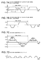
- the embodiment of the present invention by devising the sustain pulse signals applied to the X electrode and the Y electrode as the voltage waveforms shown in FIGS. 7A to 7D, and preventing the clamping of the above-described parasitic diode, the output terminal to the Z electrode is maintained in a high impedance state.
- the embodiment of the present invention will be further described below with reference to the time charts in FIGS. 7A to 7D.
- the voltage waveform of the sustain pulse signal applied to the X electrode (hereafter referred to as "X sustain signal") is shown in FIG. 7A.
- one cycle of the X sustain signal is made of a half cycle that contains a positive pulse and a half cycle that contains a negative pulse.
- the time t1' of the commencement of the rise of the negative pulse is set longer than the time t1 of the completion of the rise of the positive pulse.
- the time t2 of the commencement of the fall of the positive pulse is set longer than the time t2' of the completion of the fall of the negative pulse.
- the pulse width of the positive pulse is set wider than the pulse width of the negative pulse, but it is also possible to set the polarities of both pulses in reverse.
- the voltage waveform of the sustain pulse signal applied to the Y electrode (hereafter referred to as "Y sustain signal”) is shown in FIG. 7B.
- the Y sustain signal is displaced by a half cycle from the phase of the X sustain signal.
- X sustain signals and Y sustain signals are applied to the X electrode and the Y electrode of the discharge cell during the period of the sustain step, and therefore the change in the electric potential difference between the X electrode and the Y electrode, that is, the voltage change of (X - Y) gives the voltage waveform shown in FIG. 7C.
- the peak value of the electric potential difference between the X electrode and the Y electrode for each half cycle of the X and Y sustain signals reaches two hundred and several tens of volts, which is necessary for a sustain discharge, and a sustain discharge is induced in the discharge cell for each peak value.
- the voltage of the Z electrode during the period of the sustain step is (X + Y)/2, which is the mean of the voltages of the X electrode and the Y electrode, and therefore the voltage of the Z electrode corresponding to the X or Y sustain signal gives the voltage waveform shown in FIG. 7D.
- the voltage of the Z electrode is kept at 60 V or less even at its peak value, and it is possible to prevent clamping of the parasitic diode of the FET accommodated in the row electrode drive circuit 21.
- the switching elements contained in the circuit in FIG. 4 may be configured, for example, using a FET drain terminal and source terminal, or they may be configured using other semiconductor elements.
- ON-OFF control for the switching element is achieved by applying a control signal to the gate terminal of the FET.
- the ON-OFF condition of all the switching elements shown in FIG. 4 is controlled with control signals that are supplied from the drive control circuit 51 shown in FIG. 3.
- the various control signals supplied from the drive control circuit 51 are omitted in order to clarify the description, with simply only the changes in the ON-OFF condition of each switching element shown chronologically.
- each switching element is noted with only its reference name, as in U1XS for example.
- other elements such as capacitors and inductors are also indicated only by their reference names, as in C1 and U1XL for example.
- the S31 and the S32 of the row electrode drive circuit 21 are turned OFF, and the Z11 connected to the Z electrode of the discharge cell is in a state of high impedance.
- the U2XS of the row electrode drive circuit 41 (the X electrode drive circuit) is turned ON and the G2XS is turned OFF, so that the C4 is connected via the serial branch U2X to the X11, which is the output terminal to the X electrode.
- the C4 is charged in advance by a means (not shown in the drawings) to a predetermined electric potential, and this charging current flows via the resonance circuit U2X into the capacitance component of the discharge cell connected to the X electrode, so that the electric potential of the X electrode begins to increase due to the resonance current.
- the B2XS is turned ON at the time-point t2, the electric potential of the X electrode is clamped at the electric potential of the T5 (+Vs/2).
- the U2XS and the B2XS are turned OFF and the D2XS is turned ON, releasing the clamping of the X electrode, and now the serial branch D2X is connected to the X electrode instead of the serial branch U2X.
- the charge that is charged to the capacitance component of the discharge cell is now discharged via the resonance circuit D2X to the C4, and the electric potential of the X electrode gradually decreases.
- the D2XS is turned OFF and the G2XS is turned ON, and therefore the serial branch D2X is disconnected from the X electrode so that the electric potential of the X electrode is clamped to the ground potential via the G2XD.
- the D1XS is turned ON and the C3 is connected via the serial branch D1X to the X electrode. Since the C3 is charged in advance by a means (not shown in the drawings) to a predetermined negative electric potential, the electric potential of the X electrode is gradually reduced by the resonance current via the resonance circuit D1X. After this, at the time-point t12, the G1XS is turned ON so that the electric potential of the X electrode is clamped to the electric potential of the T6 (-Vs/2).
- the D1XS and the G1XS are turned OFF and the U1XS is turned ON, releasing the clamping of the X electrode, and now the C3 is connected to the X electrode via the serial branch U1X instead of the serial branch D1X.
- the electric potential of the X electrode gradually increases due to the power collection of the resonance circuit U1X and the C3.
- the U1XS is turned OFF and the B1XS is turned ON so that the serial branch U1X is disconnected from the X electrode and the electric potential of the X electrode is clamped to the ground potential via the B1XD.
- the voltage waveform of one cycle portion of the X sustain signal shown in FIG. 8 is generated by the above-described operation.
- the sustain signals to the Y electrode are supplied to the output terminal Y11 via the connecting line Y12 and a reset pulse-scanning pulse generating portion, but the operation of this portion has no direct relation to the present invention. Accordingly, the operation of this portion is omitted in the following description and description is given with the assumption that the connecting line Y12 is the output terminal to the Y electrode.
- the S31 and the S32 of the row electrode drive circuit 21 are turned OFF, and the Z electrode of the discharge cell is in a floating state.
- the B1YS of the row electrode drive circuit 31 (the Y electrode drive circuit) is turned OFF to release the clamping to the ground potential of the Y12.
- the D1YS is turned ON and the C1 is connected via the serial branch D1Y to the Y12. Since the C1 is charged in advance by a means (not shown in the drawings) to a predetermined negative electric potential, the electric potential of the Y12 is gradually reduced by the resonance current via the resonance circuit D1Y.
- the G1YS is turned ON so that the electric potential of the Y12 is clamped to the electric potential of the T2 (-Vs/2).
- the D1YS and the G1YS are turned OFF and the U1YS is turned ON, releasing the clamping of the Y12, and now the C1 is connected to the Y12 via serial branch U1Y instead of the serial branch D1Y.
- the electric potential of the Y12 gradually increases due to the power collection of the resonance circuit U1Y and the C1.
- the U1YS is turned OFF and the B1YS is turned ON so that the serial branch U1Y is disconnected from the Y12 and the electric potential of the Y12 is clamped to the ground potential via the B1YD.
- the U2YS is turned ON and the C2 is connected via the serial branch U2Y to the Y12.
- the C2 is charged in advance by a means (not shown in the drawings) to a predetermined electric potential, and this charging current flows via the resonance circuit U2Y into the capacitance component of the discharge cell connected to the Y electrode, so that the electric potential of the Y electrode begins to increase due to the resonance current.
- the electric potential of the Y12 is clamped to the electric potential of the T1 (+Vs/2).
- the U2YS and the B2YS are turned OFF and the D2YS is turned ON, releasing the clamping of the Y12, and now the serial branch D2Y is connected to the Y12 instead of the serial branch U2Y.
- the current that is charged to the capacitance component of the discharge cell is now discharged via the resonance circuit D2Y to the C2, and the electric potential of the Y electrode gradually decreases.
- the D2YS is turned OFF and the G2YS is turned ON, and therefore the serial branch D2Y is disconnected from the Y12 so that the electric potential of the Y electrode is clamped to the ground potential via the G2YD.
- the voltage waveform of one cycle portion of the Y sustain signal is generated.
- the above-described operation is repetitively executed during the period of the sustain step in the drive circuit shown in FIG. 4, and in this way the sustain signal shown in FIG. 8 appears cyclically in the X and Y electrodes of the discharge cell.
- the output terminal of the column electrode drive circuit can be maintained in a state of high impedance during the entire period of the sustain step, and the capacitance load of the discharge cells can be reduced, and it is therefore possible to reduce power consumption in the sustain step.
- a display panel driving method according to the present invention may also be applied, for example, to a driving sequence in which all the discharge cells are initialized to a non-light-emitting state by a reset discharge, after which wall charges are selectively formed in the addressing step by a selective writing discharge to set the light-emitting state or non-light-emitting state of each discharge cell.
Landscapes
- Engineering & Computer Science (AREA)
- Physics & Mathematics (AREA)
- Power Engineering (AREA)
- Plasma & Fusion (AREA)
- Computer Hardware Design (AREA)
- General Physics & Mathematics (AREA)
- Theoretical Computer Science (AREA)
- Control Of Indicators Other Than Cathode Ray Tubes (AREA)
- Control Of Gas Discharge Display Tubes (AREA)
- Electroluminescent Light Sources (AREA)
- Transforming Electric Information Into Light Information (AREA)
Applications Claiming Priority (2)
| Application Number | Priority Date | Filing Date | Title |
|---|---|---|---|
| JP2003112530 | 2003-04-17 | ||
| JP2003112530A JP2004317832A (ja) | 2003-04-17 | 2003-04-17 | 表示パネル駆動方法 |
Publications (2)
| Publication Number | Publication Date |
|---|---|
| EP1469446A2 true EP1469446A2 (fr) | 2004-10-20 |
| EP1469446A3 EP1469446A3 (fr) | 2008-04-02 |
Family
ID=32906057
Family Applications (1)
| Application Number | Title | Priority Date | Filing Date |
|---|---|---|---|
| EP04251875A Withdrawn EP1469446A3 (fr) | 2003-04-17 | 2004-03-30 | Procédé de commande d'un panneau d'affichage |
Country Status (6)
| Country | Link |
|---|---|
| US (1) | US7605781B2 (fr) |
| EP (1) | EP1469446A3 (fr) |
| JP (1) | JP2004317832A (fr) |
| KR (1) | KR100589882B1 (fr) |
| CN (1) | CN1538370A (fr) |
| TW (1) | TWI265470B (fr) |
Cited By (1)
| Publication number | Priority date | Publication date | Assignee | Title |
|---|---|---|---|---|
| EP1844461A4 (fr) * | 2005-01-24 | 2009-05-27 | Ifire Ip Corp | Pilote de colonnes a faible consommation d'energie pour affichages electroluminescents |
Families Citing this family (6)
| Publication number | Priority date | Publication date | Assignee | Title |
|---|---|---|---|---|
| JP4603879B2 (ja) * | 2004-12-28 | 2010-12-22 | 日立プラズマディスプレイ株式会社 | プラズマディスプレイパネルの駆動方法および駆動回路、並びに、プラズマディスプレイ装置 |
| KR100667558B1 (ko) * | 2005-06-24 | 2007-01-12 | 엘지전자 주식회사 | 플라즈마 디스플레이 장치 및 그 구동 방법 |
| CN100424738C (zh) * | 2005-12-01 | 2008-10-08 | 帆宣系统科技股份有限公司 | 高分辨率的对向放电型等离子平面显示器的驱动方法 |
| KR100800499B1 (ko) * | 2006-07-18 | 2008-02-04 | 엘지전자 주식회사 | 플라즈마 디스플레이 장치 |
| TWI486932B (zh) * | 2013-04-03 | 2015-06-01 | Himax Tech Inc | 面板驅動電路 |
| CN104714319B (zh) * | 2014-12-23 | 2017-11-14 | 上海中航光电子有限公司 | 一种液晶显示面板及其显示装置 |
Family Cites Families (11)
| Publication number | Priority date | Publication date | Assignee | Title |
|---|---|---|---|---|
| DE3331690A1 (de) * | 1983-09-02 | 1985-04-04 | Aeg Elotherm Gmbh | Parallelschwingkreisumrichter |
| US5081400A (en) * | 1986-09-25 | 1992-01-14 | The Board Of Trustees Of The University Of Illinois | Power efficient sustain drivers and address drivers for plasma panel |
| JP2772753B2 (ja) | 1993-12-10 | 1998-07-09 | 富士通株式会社 | プラズマディスプレイパネル並びにその駆動方法及び駆動回路 |
| JPH08123362A (ja) | 1994-10-28 | 1996-05-17 | Noritake Co Ltd | プラズマディスプレイパネルの駆動方法 |
| JP3522013B2 (ja) | 1995-09-04 | 2004-04-26 | 富士通株式会社 | 画像表示装置、および画像表示装置の駆動方法 |
| JP3591766B2 (ja) | 1998-11-20 | 2004-11-24 | パイオニア株式会社 | Pdp駆動装置 |
| JP2000172228A (ja) * | 1998-12-01 | 2000-06-23 | Mitsubishi Electric Corp | Ac放電を利用した表示パネルの駆動方法 |
| JP2000242223A (ja) | 1999-02-23 | 2000-09-08 | Matsushita Electric Ind Co Ltd | プラズマディスプレイパネルの駆動方法及びそれを用いたディスプレイ装置 |
| JP3201603B1 (ja) | 1999-06-30 | 2001-08-27 | 富士通株式会社 | 駆動装置、駆動方法およびプラズマディスプレイパネルの駆動回路 |
| JP5031952B2 (ja) | 2001-06-27 | 2012-09-26 | 株式会社日立製作所 | プラズマディスプレイ |
| KR100431559B1 (ko) * | 2001-07-03 | 2004-05-12 | 주식회사 유피디 | 에너지 회수 회로를 구비한 교류형 플라즈마 디스플레이패널의 유지 구동 장치 |
-
2003
- 2003-04-17 JP JP2003112530A patent/JP2004317832A/ja active Pending
-
2004
- 2004-03-23 US US10/806,449 patent/US7605781B2/en not_active Expired - Fee Related
- 2004-03-29 TW TW093108534A patent/TWI265470B/zh not_active IP Right Cessation
- 2004-03-30 EP EP04251875A patent/EP1469446A3/fr not_active Withdrawn
- 2004-04-08 KR KR1020040024229A patent/KR100589882B1/ko not_active Expired - Fee Related
- 2004-04-14 CN CNA2004100328718A patent/CN1538370A/zh active Pending
Cited By (1)
| Publication number | Priority date | Publication date | Assignee | Title |
|---|---|---|---|---|
| EP1844461A4 (fr) * | 2005-01-24 | 2009-05-27 | Ifire Ip Corp | Pilote de colonnes a faible consommation d'energie pour affichages electroluminescents |
Also Published As
| Publication number | Publication date |
|---|---|
| KR20040090703A (ko) | 2004-10-26 |
| US7605781B2 (en) | 2009-10-20 |
| TWI265470B (en) | 2006-11-01 |
| EP1469446A3 (fr) | 2008-04-02 |
| TW200425010A (en) | 2004-11-16 |
| CN1538370A (zh) | 2004-10-20 |
| JP2004317832A (ja) | 2004-11-11 |
| KR100589882B1 (ko) | 2006-06-19 |
| US20040207616A1 (en) | 2004-10-21 |
Similar Documents
| Publication | Publication Date | Title |
|---|---|---|
| US20120001836A1 (en) | Plasma display device | |
| EP1469446A2 (fr) | Procédé de commande d'un panneau d'affichage | |
| US7345662B2 (en) | Apparatus for driving capacitive light emitting elements | |
| US7586486B2 (en) | Display panel driving apparatus | |
| US6480189B1 (en) | Display panel driving apparatus | |
| JP2003233343A (ja) | 表示パネル駆動回路 | |
| US7609233B2 (en) | Plasma display device and driving apparatus thereof | |
| CN100492454C (zh) | 等离子体显示设备及其驱动装置和驱动方法 | |
| EP2136351A1 (fr) | Appareil d'affichage à plasma et procédé de commande correspondant pour empêcher les effets negatifs de fréquences de résonance non souhaitées | |
| KR100648685B1 (ko) | 플라즈마 표시 장치 및 그 구동 장치와 구동 방법 | |
| KR100740093B1 (ko) | 플라즈마 표시 장치 및 그 구동 장치와 구동 방법 | |
| US20090115699A1 (en) | Plasma display and driving method thereof | |
| KR100818198B1 (ko) | 평면 표시 장치 | |
| US7612738B2 (en) | Plasma display device, apparatus for driving the same, and method of driving the same | |
| KR20040033170A (ko) | 플라즈마 디스플레이 패널의 구동 방법 | |
| KR100805112B1 (ko) | 플라즈마 표시 장치 및 그 구동 방법 | |
| KR100649526B1 (ko) | 플라즈마 표시 장치 및 그 구동 방법 | |
| US20060164337A1 (en) | Device for driving capacitive light-emitting elements | |
| US20060192731A1 (en) | Plasma display device | |
| US20070091026A1 (en) | Plasma display device and driving method thereof | |
| US20070120774A1 (en) | Plasma display, driving device, and driving method | |
| US20070097033A1 (en) | Driving of plasma display device | |
| US20070120532A1 (en) | Driving device and method of driving plasma displays | |
| US20080158219A1 (en) | Plasma display device, driving device, and method of driving the same | |
| EP2113902A2 (fr) | Dispositif à écran plasma et procédé de commande associé |
Legal Events
| Date | Code | Title | Description |
|---|---|---|---|
| PUAI | Public reference made under article 153(3) epc to a published international application that has entered the european phase |
Free format text: ORIGINAL CODE: 0009012 |
|
| AK | Designated contracting states |
Kind code of ref document: A2 Designated state(s): AT BE BG CH CY CZ DE DK EE ES FI FR GB GR HU IE IT LI LU MC NL PL PT RO SE SI SK TR |
|
| AX | Request for extension of the european patent |
Extension state: AL LT LV MK |
|
| PUAL | Search report despatched |
Free format text: ORIGINAL CODE: 0009013 |
|
| AK | Designated contracting states |
Kind code of ref document: A3 Designated state(s): AT BE BG CH CY CZ DE DK EE ES FI FR GB GR HU IE IT LI LU MC NL PL PT RO SE SI SK TR |
|
| AX | Request for extension of the european patent |
Extension state: AL LT LV MK |
|
| AKX | Designation fees paid |
Designated state(s): DE FR GB |
|
| STAA | Information on the status of an ep patent application or granted ep patent |
Free format text: STATUS: THE APPLICATION IS DEEMED TO BE WITHDRAWN |
|
| 18D | Application deemed to be withdrawn |
Effective date: 20081003 |