EP2136351A1 - Appareil d'affichage à plasma et procédé de commande correspondant pour empêcher les effets negatifs de fréquences de résonance non souhaitées - Google Patents
Appareil d'affichage à plasma et procédé de commande correspondant pour empêcher les effets negatifs de fréquences de résonance non souhaitées Download PDFInfo
- Publication number
- EP2136351A1 EP2136351A1 EP09251225A EP09251225A EP2136351A1 EP 2136351 A1 EP2136351 A1 EP 2136351A1 EP 09251225 A EP09251225 A EP 09251225A EP 09251225 A EP09251225 A EP 09251225A EP 2136351 A1 EP2136351 A1 EP 2136351A1
- Authority
- EP
- European Patent Office
- Prior art keywords
- capacitor
- terminal
- voltage
- inductor
- coupled
- Prior art date
- Legal status (The legal status is an assumption and is not a legal conclusion. Google has not performed a legal analysis and makes no representation as to the accuracy of the status listed.)
- Withdrawn
Links
Images



Classifications
-
- G—PHYSICS
- G09—EDUCATION; CRYPTOGRAPHY; DISPLAY; ADVERTISING; SEALS
- G09G—ARRANGEMENTS OR CIRCUITS FOR CONTROL OF INDICATING DEVICES USING STATIC MEANS TO PRESENT VARIABLE INFORMATION
- G09G3/00—Control arrangements or circuits, of interest only in connection with visual indicators other than cathode-ray tubes
- G09G3/20—Control arrangements or circuits, of interest only in connection with visual indicators other than cathode-ray tubes for presentation of an assembly of a number of characters, e.g. a page, by composing the assembly by combination of individual elements arranged in a matrix no fixed position being assigned to or needed to be assigned to the individual characters or partial characters
- G09G3/22—Control arrangements or circuits, of interest only in connection with visual indicators other than cathode-ray tubes for presentation of an assembly of a number of characters, e.g. a page, by composing the assembly by combination of individual elements arranged in a matrix no fixed position being assigned to or needed to be assigned to the individual characters or partial characters using controlled light sources
- G09G3/28—Control arrangements or circuits, of interest only in connection with visual indicators other than cathode-ray tubes for presentation of an assembly of a number of characters, e.g. a page, by composing the assembly by combination of individual elements arranged in a matrix no fixed position being assigned to or needed to be assigned to the individual characters or partial characters using controlled light sources using luminous gas-discharge panels, e.g. plasma panels
- G09G3/288—Control arrangements or circuits, of interest only in connection with visual indicators other than cathode-ray tubes for presentation of an assembly of a number of characters, e.g. a page, by composing the assembly by combination of individual elements arranged in a matrix no fixed position being assigned to or needed to be assigned to the individual characters or partial characters using controlled light sources using luminous gas-discharge panels, e.g. plasma panels using AC panels
- G09G3/296—Driving circuits for producing the waveforms applied to the driving electrodes
- G09G3/2965—Driving circuits for producing the waveforms applied to the driving electrodes using inductors for energy recovery
-
- G—PHYSICS
- G09—EDUCATION; CRYPTOGRAPHY; DISPLAY; ADVERTISING; SEALS
- G09G—ARRANGEMENTS OR CIRCUITS FOR CONTROL OF INDICATING DEVICES USING STATIC MEANS TO PRESENT VARIABLE INFORMATION
- G09G3/00—Control arrangements or circuits, of interest only in connection with visual indicators other than cathode-ray tubes
- G09G3/20—Control arrangements or circuits, of interest only in connection with visual indicators other than cathode-ray tubes for presentation of an assembly of a number of characters, e.g. a page, by composing the assembly by combination of individual elements arranged in a matrix no fixed position being assigned to or needed to be assigned to the individual characters or partial characters
- G09G3/22—Control arrangements or circuits, of interest only in connection with visual indicators other than cathode-ray tubes for presentation of an assembly of a number of characters, e.g. a page, by composing the assembly by combination of individual elements arranged in a matrix no fixed position being assigned to or needed to be assigned to the individual characters or partial characters using controlled light sources
- G09G3/28—Control arrangements or circuits, of interest only in connection with visual indicators other than cathode-ray tubes for presentation of an assembly of a number of characters, e.g. a page, by composing the assembly by combination of individual elements arranged in a matrix no fixed position being assigned to or needed to be assigned to the individual characters or partial characters using controlled light sources using luminous gas-discharge panels, e.g. plasma panels
- G09G3/288—Control arrangements or circuits, of interest only in connection with visual indicators other than cathode-ray tubes for presentation of an assembly of a number of characters, e.g. a page, by composing the assembly by combination of individual elements arranged in a matrix no fixed position being assigned to or needed to be assigned to the individual characters or partial characters using controlled light sources using luminous gas-discharge panels, e.g. plasma panels using AC panels
- G09G3/291—Control arrangements or circuits, of interest only in connection with visual indicators other than cathode-ray tubes for presentation of an assembly of a number of characters, e.g. a page, by composing the assembly by combination of individual elements arranged in a matrix no fixed position being assigned to or needed to be assigned to the individual characters or partial characters using controlled light sources using luminous gas-discharge panels, e.g. plasma panels using AC panels controlling the gas discharge to control a cell condition, e.g. by means of specific pulse shapes
Definitions
- the present invention relates to a plasma display and a driving apparatus thereof.
- a plasma display includes a display panel having a plurality of display electrodes and a plurality of discharge cells defined by the display electrodes.
- the display electrodes for example, include address electrodes, scan electrodes and sustain electrodes.
- the plasma display displays an image by applying a sustain pulse having a high level voltage and a low level voltage alternately to a pair of display electrodes (e.g., sustain electrodes) to perform a sustain discharge for sustain-discharging a cell that is defined by the pair of display electrodes to emit light.
- the cell will be referred to as a light emitting cell.
- a capacitive component (hereinafter referred to as "a panel capacitor") is formed by the pair of display electrodes where the sustain discharge is generated, a reactive power is generated when the high level voltage and the low level voltage are respectively applied to the pair of display electrodes.
- a typical plasma display may include an energy recovery circuit for reusing (or recovering) the reactive power.
- the energy recovery circuit includes an energy recovery capacitor and an inductor that is electrically coupled between a panel capacitor and the energy recovery capacitor.
- the energy recovery circuit generates a resonance between the inductor and the panel capacitor, recovers a resonant current corresponding to a discharge in the panel capacitor to the energy recovery capacitor, and supplies the resonant current for charging the panel capacitor from the energy recovery capacitor.
- a plurality of capacitors each having the same capacitance and coupled in parallel, may be used as the energy recovery capacitor.
- a variation e.g., capacitance, parasitic inductance
- a variation may exist between the plurality of capacitors coupled in parallel, or a variation may exist between parasitic inductive components that may be represented as inductors respectively coupled to the plurality of capacitors in series.
- a resonance cycle i.e., an inverse number of a resonance frequency
- a resonance cycle of the first capacitor and the inductor is different from a resonance cycle of the second capacitor and the inductor so that the amount of current flowing to the first capacitor and the amount of current flowing to the second capacitor may differ from each other at the end of their resonance cycles.
- a resonance is generated again through a closed loop that is formed by the first capacitor, the parasitic inductive component coupled to the first capacitor, the second capacitor, and the parasitic inductive component coupled to the second capacitor so that a resonance current may flow through the closed loop.
- the parasitic inductive component coupled to the first capacitor and the parasitic inductive component coupled to the second capacitor may have different inductances.
- the resonance cycle corresponding to the first capacitor and the inductor, and the resonance cycle corresponding to the second capacitor and the inductor become different from each other due to the variation of the parasitic inductive components so that the resonance may still occur through the closed loop.
- the resonance cycle is proportional to a square root of the product of the capacitance of the capacitor and the inductance of the inductor in the resonance path.
- the capacitance of each of the first and second capacitors is set (or configured) to be larger than that of the panel capacitor, and the inductance of the inductor is set (or configured) to be larger than that of the parasitic inductive component in the energy recovery circuit. Therefore, a resonance cycle formed by the first and second capacitors and their parasitic inductive components in the closed loop may be similar to a resonance cycle formed by the panel capacitor and the inductor.
- the resonance current in the closed loop may reach a maximum value during a period in which the high level voltage or the low level voltage is applied (i.e., maintained) to the display electrode. Accordingly, a large resonance current is repeatedly supplied to the first and second capacitors while the period is repeated so that temperatures of the first and second capacitors may increase, thereby causing overheating of the energy recovery circuit or degradation of the first and second capacitors.
- Embodiments of the present invention provide a plasma display and a driving device thereof for reducing resonances between a plurality of capacitors that form an energy recovery circuit.
- a plasma display includes a display electrode and an energy recovery circuit that includes an energy recovery capacitor.
- the energy recovery circuit is configured to form a first path between the energy recovery capacitor and the display electrode to change a voltage at the display electrode in a sustain period.
- the energy recovery capacitor includes a plurality of capacitors configured to be charged concurrently.
- a second path is formed between the plurality of capacitors, and a product of an inductance formed on the second path and a capacitance formed on the second path is greater than twice a product of an inductance formed on the first path and a capacitance formed on the first path.
- a plasma display includes a display electrode, a first capacitor, a second capacitor, a first inductor, a second inductor, and a switching circuit.
- the first capacitor has a first terminal coupled to a ground terminal and a second terminal.
- the second capacitor has a first terminal coupled to the ground terminal and a second terminal.
- the first inductor has a first terminal coupled to the second terminal of the first capacitor and a second terminal.
- the second inductor has a first terminal coupled to the second terminal of the second capacitor and a second terminal.
- the switching circuit is coupled between the display electrode and the second terminals of the first inductor and second inductor, and configured to couple the first capacitor to the display electrode via the first inductor and couple the second capacitor to the display electrode via the second inductor concurrently to increase a voltage at the display electrode in a sustain period.
- a plasma display includes a plasma display panel, a first inductor, a second inductor, a first capacitor coupled to the plasma display panel via the first inductor, and a second capacitor coupled to the plasma display panel via the second inductor.
- a first terminal of each of the first capacitor and the second capacitor is grounded, and a second terminal of the first capacitor is electrically coupled to a second terminal of the second capacitor via the first inductor and the second inductor.
- the first capacitor and the second capacitor are configured to be charged concurrently.
- a plasma display has a plurality of display electrodes and a driver for driving the plurality of display electrodes.
- the driver includes a first switch, a second switch, a plurality of capacitors, a plurality of first inductors, and a third switch.
- the first switch is coupled between a display electrode of the plurality of display electrodes and a first power source for supplying a first voltage in a sustain period.
- the second switch is coupled between the display electrode and a second power source for supplying a second voltage that is lower than the first voltage in the sustain period.
- the plurality of capacitors each have a first terminal coupled to a third power source, and the plurality of capacitors are configured to be charged concurrently.
- the plurality of first inductors each have a first terminal coupled to a second terminal of a corresponding one of the plurality of capacitors, and the third switch is coupled between second terminals of the plurality of first inductors and the display electrode.
- a plasma display has a plurality of display electrodes and a driver for driving the plurality of display electrodes.
- the driver includes a first switch, a second switch, a plurality of capacitors, a plurality of inductors, a third switch, and a fourth switch.
- the first switch is coupled between a display electrode of the plurality of display electrodes and a first power source for supplying a first voltage in a sustain period.
- the second switch is coupled between the display electrode and a second power source for supplying a second voltage that is lower than the first voltage in the sustain period.
- the plurality of capacitors each have a first terminal coupled to a third power source, and the plurality of capacitors are configured to be charged concurrently.
- the plurality of first inductors each have a first terminal coupled to a second terminal of a corresponding one of the plurality of capacitors and a second terminal.
- the third switch is coupled between second terminals of the plurality of first inductors and the display electrode, and the fourth switch is coupled between the second terminals of the plurality of first inductors and the display electrode.
- a plasma display has a plurality of display electrodes and a driver for driving the plurality of display electrodes
- the driver includes a first switch, a second switch, a plurality of capacitors, a plurality of first inductors, a plurality of second inductors, a third switch, and a fourth switch.
- the first switch is coupled between a display electrode of the plurality of display electrodes and a first power source for supplying a first voltage in a sustain period.
- the second switch is coupled between the display electrode and a second power source for supplying a second voltage that is lower than the first voltage in the sustain period.
- the plurality of capacitors each have a first terminal coupled to a third power source, and the plurality of capacitors are configured to be charged concurrently.
- the plurality of first inductors each have a first terminal coupled to a second terminal of a corresponding one of the plurality of capacitors and a second terminal.
- the plurality of second inductors each have a first terminal coupled to the second terminal of a corresponding one of the plurality of capacitors and a second terminal.
- the third switch is coupled between second terminals of the plurality of first inductors and the display electrode.
- the fourth switch is coupled between second terminals of the plurality of second inductors and the display electrode.
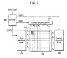
- FIG. 1 is a schematic block diagram of a plasma display according to an embodiment of the present invention
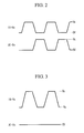
- FIG. 2 and FIG. 3 respectively show driving waveforms in a sustain period of a plasma display according to an embodiment of the present invention.
- a plasma display includes a plasma display panel 100, a controller 200, an address electrode driver 300, a scan electrode driver 400, and a sustain electrode driver 500.
- the plasma display panel 100 includes a plurality of display electrodes Y1 to Yn and X1 to Xn, a plurality of address electrodes (hereinafter referred to as "A electrodes") A1 to Am, and a plurality of discharge cells 110.
- Y1 to Yn are scan electrodes (hereinafter referred to as "Y electrodes")
- X1 to Xn are sustain electrodes (hereinafter referred to as "X electrodes”).
- the Y electrodes Y1 to Yn and the X electrodes X1 to Xn extend in a row direction and form substantially parallel pairs of Y and X electrodes.
- the A electrodes A1 to Am extend in a column direction crossing the row direction and are substantially parallel to each other.
- Each of the Y electrodes Y1 to Yn may correspond to one of the X electrodes X1 to Xn, or one of the Y electrodes Y1 to Yn may correspond to two of the X electrodes X1 to Xn.
- discharge cells 110 are formed in spaces defined at the crossings of the A electrodes A1 to Am, the Y electrodes Y1 to Yn, and the X electrodes X1 to Xn.
- the above-described plasma display panel 100 is only one example, and the plasma display panel 100 may have other structures according to embodiments of the present invention.
- the controller 200 receives a video signal and an input control signal for controlling the display of the video signal.
- the video signal includes luminance information of each of the discharge cells 110, and the luminance of each of the discharge cells 110 may be represented as one of a number of gray levels.
- the input control signal may include a vertical synchronization signal and a horizontal synchronization signal.
- the controller 200 divides one frame for displaying an image into a plurality of subfields, each of which has a luminance weight and includes an address period and a sustain period.
- the controller 200 processes the video signal and the input control signal based on the plurality of subfields, and generates an A electrode driving control signal CONT1, a Y electrode driving control signal CONT2, and an X electrode driving control signal CONT3.
- the controller 200 outputs the A electrode driving control signal CONT1 to the address electrode driver 300, the Y electrode driving control signal CONT2 to the scan electrode driver 400, and the X electrode driving control signal CONT3 to the sustain electrode driver 500.
- the controller 200 changes or converts the video signal that corresponds to each of the discharge cells 110 into subfield data that indicate a light emitting/non-light emitting state of each of the discharge cells 110 in the plurality of subfields, and the A electrode driving control signal CONT1 includes the subfield data.
- the Y electrode driving control signal CONT2 and the X electrode driving control signal CONT3 include a sustain discharge control signal that controls the number of sustain discharge occurrences and/or sustain discharge operations in the sustain period of each subfield.
- the Y electrode driving control signal CONT2 further includes a scan control signal that controls a scan operation in the address period of each subfield.
- the scan electrode driver 400 sequentially applies a scan voltage to the Y electrodes Y1 to Yn in the address period according to the Y electrode driving control signal CONT2.
- the address electrode driver 300 applies a voltage to the A electrodes A1 to Am in accordance with the A electrode driving control signal CONT1 for identifying light emitting cells and non-light emitting cells from the plurality of discharge cells 110 coupled to the Y electrodes to which the scan voltage is applied.
- the scan electrode driver 400 and the sustain electrode driver 500 alternately apply a sustain pulse to the Y electrodes Y1 to Yn and the X electrodes X1 to Xn a number of times that correspond to a luminance weight of each subfield during the sustain period in accordance with the Y electrode driving control signal CONT2 and the X electrode driving control signal CONT3.
- FIG. 2 is a schematic drawing showing driving waveforms in a sustain period of a plasma display according to an embodiment of the present invention.
- the sustain pulses having a high level voltage Vs and a low level voltage are alternately applied to the Y electrodes Y1 to Yn and the X electrodes X1 to Xn.
- FIG. 3 is a schematic drawing showing driving waveforms in a sustain period of a plasma display according to an embodiment of the present invention.
- sustain pulses having the high level voltage Vs and a low level voltage -Vs are applied only to the Y electrodes Y1 to Yn while a suitable voltage (e.g., a predetermined voltage, OV) is applied to the X electrodes X1 to Xn.
- a suitable voltage e.g., a predetermined voltage, OV
- the sustain pulses having the high level voltage Vs and the low level voltage -Vs may be applied only to the X electrodes X1 to Xn while a suitable voltage is applied to the Y electrodes Y1 to Yn according to an embodiment of the present invention.
- the sustain discharges may occur in the discharge cells 110 by setting a voltage difference between the high level voltage Vs and the suitable voltage and a voltage difference between the low level voltage -Vs and the suitable voltage to be similar to the voltage difference between the high level voltage Vs and the low level voltage (e.g., OV) of FIG. 2 .
- a sustain discharge circuit that generates a driving waveform (i.e., sustain pulses) in a sustain period of the plasma display will now be described in further detail with reference to FIG. 4 .
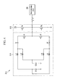
- FIG. 4 is a schematic circuit diagram of a sustain discharge circuit according to an embodiment of the present invention.
- a sustain discharge circuit 510 includes a voltage sustain unit 512 and an energy recovery circuit 514.
- the sustain discharge circuit 510 may be included in the sustain electrode driver 500, and is commonly coupled to all or some of the plurality of X electrodes X1 to Xn.
- the sustain discharge circuit 510 may be included in the scan electrode driver 400, and may be commonly coupled to all or some of the plurality of Y electrodes Y1 to Yn.
- the sustain discharge circuit 510 is shown to be coupled to the X electrodes, and only one of the X electrodes X1 to Xn is shown.
- a capacitive component formed by the X electrode and a Y electrode is illustrated as a capacitor (hereinafter referred to as a "panel capacitor").
- the voltage sustain unit 512 includes transistors Xs and Xg for applying the high level voltage Vs and the low level voltage, respectively, to the X electrode.
- the energy recovery circuit 514 includes transistors Xr and Xf, diodes Dr and Df, a plurality of rising inductors Lr1 and Lr2, a plurality of falling inductors Lf1 and Lf2, and a plurality of capacitors C1 and C2.
- the energy recovery circuit 514 is operated to form a path for increasing a voltage of the X electrode or a path for decreasing the voltage of the X electrode.
- Each of the transistors Xs, Xg, Xr, and Xf is a switch including a control terminal, an input terminal, and an output terminal.
- the transistors Xs, Xg, Xr, and Xf are respectively illustrated as an N-channel field effect transistor (FET), and in the embodiment shown in FIG. 4 , the control terminal, the input terminal, and the output terminal respectively correspond to a gate, a drain, and a source.
- FET field effect transistor
- Each of the transistors Xs, Xg, Xr, and Xf may include a body diode (not shown), and an anode of the body diode is coupled to a source of a corresponding one of the transistors Xs, Xg, Xr, and Xf.
- a cathode of the body diode is coupled to a drain of a corresponding one of the transistors Xs, Xg, Xr, and Xf.
- Each of the transistors Xs, Xg, Xr, and Xf receives a control signal (not shown) for controlling their operation through their gates, and the control signal may be applied by the sustain electrode driver 500 according to the X electrode control signal CONT3.
- the drain of the transistor Xs is coupled to a power source that supplies the high level voltage Vs, and the source of the transistor Xs is coupled to the X electrode.
- the drain of the transistor Xg is coupled to the X electrode, and the source of the transistor Xg is coupled to a power source (e.g., a ground terminal) that supplies the low level voltage.
- the source of the transistor Xr is coupled to the X electrode, and the drain of the transistor Xr is coupled to a cathode of the diode Dr.
- the drain of the transistor Xf is coupled to the X electrode, and the source of the transistor Xf is coupled to an anode of the diode Df.
- the serial connection order of the transistor Xr and the diode Dr and the serial connection order of the transistor Xf and the diode Df may be switched with each other.
- the cathode of the diode Dr may be coupled to the X electrode
- the source of the transistor Xr may be coupled to the anode of the diode Dr
- the anode of the diode Df may be coupled to the X electrode
- the drain of the transistor Xf may be coupled to the cathode of the diode Df.
- the transistor Xr and the diode Dr form a current path for charging the panel capacitor (i.e., for increasing the voltage of the X electrode), and the transistor Xf and the diode Df form another current path for discharging the panel capacitor (i.e., for decreasing the voltage of the X electrode). That is, the transistors Xr and Xf, and the diodes Dr and Df form at least one switching circuit for increasing or decreasing the voltage of the X electrode.
- the diodes Dr and Df respectively block (e.g., disconnect) backward current paths that can be formed by the body diodes of the transistors Xr and Xf. In some embodiments of the present invention, the current paths are not formed in a direction from the source to the drain of the transistors Xr and Xf, therefore the diodes Dr and Df may be eliminated.
- the plurality of capacitors C1 and C2 form an energy recovery capacitor, and although FIG. 4 illustrates two capacitors for ease of description, three or more capacitors may form the energy recovery capacitor.
- One terminal of each of the plurality of capacitors C1 and C2 is coupled to a power source that supplies a suitable low level voltage (e.g., a predetermined voltage).
- the plurality of capacitors C1 and C2 may store a voltage between the high level voltage Vs and the low level voltage, for example, a voltage at approximately half the voltage difference between the high level voltage Vs and the low level voltage.
- One terminal of each of the rising inductors Lr1 and Lr2 is coupled to the anode of the diode Dr, another terminal of the rising inductor Lr1 is coupled to another terminal of the capacitor C1, and another terminal of the rising inductor Lr2 is coupled to another terminal of the capacitor C2.
- One terminal of each of the falling inductors Lf1 and Lf2 is coupled to the cathode of the diode Df, another terminal of the falling inductor Lf1 is coupled to the another terminal of the capacitor C1, and another terminal of the falling inductor Lf2 is coupled to the another terminal of the capacitor C2.
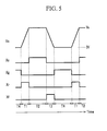
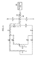
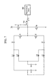
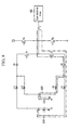
- FIG. 5 is a schematic drawing showing signal timings of the sustain discharge circuit 510 according to an embodiment of the present invention, and FIG. 6 to FIG. 9 respectively illustrate current paths of the sustain discharge circuit 510 in each of the periods shown in FIG. 5 .
- voltages of the control signals respectively applied to the gate of each of the transistors Xs, Xg, Xr, and Xf are illustrated to indicate turn-on/turn-off states of the transistors Xs, Xg, Xr, and Xf.
- the transistors Xs, Xg, Xr, and Xf are turned on when the voltages of the control signals are at a high level and turned off when the voltages of the control signals are at a low level.
- a resonance is generated between the rising inductor Lr1 and the panel capacitor in a current path 610 that includes the capacitor C1, the rising inductor Lr1, the diode Dr, the transistor Xr, and the X electrode; and a resonance is generated between the rising inductor Lr2 and the panel capacitor in a current path 620 that includes the capacitor C2, the rising inductor Lr2, the diode Dr, the transistor Xr, and the X electrode.
- a voltage Vx of the X electrode is gradually increased due to the resonances.
- the capacitors C1 and C2 are concurrently discharged by the current paths 610 and 620.
- the transistor Xs When the voltage Vx of the X electrode almost or substantially reaches the high level voltage Vs, the transistor Xs is turned on by a high level voltage as shown in FIG. 5 so that a high level voltage maintaining period T2 begins. During the high level voltage maintaining period T2, the high level voltage Vs is applied to the X electrode through a current path 710 shown in FIG. 7 so that the voltage Vx of the X electrode is maintained at the high level voltage Vs.
- the transistor Xr may be turned off by a low level voltage at the starting point of or during the high level voltage maintaining period T2.
- a resonance is generated between the falling inductor Lf1 and the panel capacitor in a current path 810 that includes the X electrode, the transistor Xf, the diode Df, the falling inductor Lf1, and the capacitor C1; and a resonance is also generated between the falling inductor Lf2 and the panel capacitor in a current path 820 that includes the X electrode, the transistor Xf, the diode Df, the falling inductor Lf2, and the capacitor C2.
- the voltage Vx of the X electrode is gradually decreased due to the resonances generated in the current paths 810 and 820.
- the capacitors C1 and C2 are concurrently charged by the current paths 810 and 820.
- the transistor Xg when the voltage Vx of the X electrode is decreased to be substantially close to the low level voltage, the transistor Xg is turned on by a high level voltage so that a low level voltage maintaining period T4 begins. During the low level maintaining period T4, the low level voltage is applied to the X electrode through a current path 910 shown in FIG. 9 to maintain the voltage Vx of the X electrode at the low level voltage.
- the transistor Xf may be turned off by a low level voltage at the starting point of or during the low level voltage maintaining period T4.
- the high level voltage Vs and the low level voltage can be alternately applied to the X electrode by repeating the periods T1 to T4.
- the scan electrode driver 400 may apply the low level voltage to the Y electrode during the high level voltage maintaining period T2, and may apply the high level voltage Vs to the Y electrode during the low level voltage maintaining period T4.
- a resonance cycle in the current path 610 may be different from a resonance cycle in the current path 620.
- the current supplied to the X electrode in the rising period T1 is a sum of the currents supplied from the two capacitors C1 and C2, however, the sum of the currents may include a current that flows to the capacitor C1 and a current that flows from the capacitor C2 even though the current supplied to the X electrode at the finishing point of the rising period T1 is substantially OA.
- a resonance path may be formed through a closed loop that includes the capacitor C1, the rising inductors Lr1 and Lr2, and the capacitor C2 even though the resonances between the panel capacitor and the rising inductors Lr1 and Lr2 are terminated.
- Capacitance of each of the capacitors C1 and C2 is set to be suitably large so that the capacitance of the panel capacitor can be ignored when the capacitors C1 and C2 are operated as a source for supplying a constant voltage in the sustain discharge circuit 510.
- a capacitive component that forms the resonance in each of the current paths 610 and 620 in the rising period T1 is determined by the capacitance of the panel capacitor, and a capacitive component that forms the resonance in the closed loop is determined by the capacitances of the capacitors C1 and C2.
- a resonance cycle T in a resonance path is proportional to a square root of the product of the capacitance C of a capacitor and the inductance L of an inductor that form the resonance path as given in Equation 1, the resonance cycle T in the closed loop is much longer than the resonance cycle T in each of the current paths 610 and 620 in the rising period T1.
- the resonance cycle T of the closed loop is greater than twice the resonance cycle of a rising resonance path , e.g., current paths 610 and 620.
- the resonance cycle T of the closed loop is a product of an inductance and a capacitance formed on the closed loop
- the resonance cycle T of the rising resonance path is a product of an inductance and a capacitance formed on the rising resonance path.
- the LC term of Equation 1 can be represented as (Lr1+Lr2)C1C2/(C1+C2) for the closed loop, and represented as [(Lr1 Lr2)/(Lr1 +Lr2)](Cp) for the rising resonance path, where Cp represents the panel capacitor, when the inductance of the parasitic inductive component of each of the capacitors C1 and C2 is sufficiently small compared to each of the inductance Lr1 and Lr2.
- the LC term can be represented as Lr1 C1 for the closed loop, and represented as Lr1 Cp/2 for the rising resonance path. Since the capacitance C1 is greater than capacitance Cp, the LC term of the closed loop is greater than twice the LC term of the rising resonance path.
- the panel capacitor has a capacitance of 100nF
- each of the capacitors C1 and C2 has a capacitance of 2.2 ⁇ F
- each of the inductors Lr1 and Lr2 has an inductance of 0.6 ⁇ H
- the resonance cycle T in each of the current paths 610 and 620 in the rising period T1 becomes approximately 1 ⁇ s
- the resonance cycle T in the closed loop that includes the capacitor C1, the rising inductors Lr1 and Lr2, and the capacitor C2 becomes approximately 5 ⁇ s.
- the resonance cycle T in the closed loop (e.g., in the period T2) is longer than the resonance cycle T in the rising period T1
- the resonance current does not reach a maximum value during the high level voltage maintaining period T2. Therefore, the resonance current is at a suitably small value to prevent the temperature of each of the capacitors C1 and C2 from being increased even though the resonance may be generated through the closed loop.
- a resonance path may be formed through the closed loop that includes the capacitor C1, the falling inductors Lf1 and Lf2, and the capacitor C2 at the finishing point of the falling period T3; therefore, the temperature of each of the capacitors C1 and C2 may be prevented from being increased since the closed loop has a long resonance cycle.
- the high level voltage is set to the Vs voltage
- the low level voltage is set to 0V in order to generate the sustain pulse of FIG. 2 .
- the high level voltage may be set to the Vs voltage
- the low level voltage may be set to the -Vs voltage for generating the sustain pulse on the Y electrodes Y1-Yn as shown in FIG. 3 .
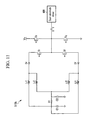
- FIG. 10 to FIG. 12 are schematic drawings that respectively illustrate circuit diagrams of sustain discharge circuits according to other embodiments of the present invention.
- the rising inductor e.g., Lr1 and Lr2 of FIG. 4
- the falling inductor e.g., Lf1 and Lf2 of FIG. 4
- single inductors e.g., L1 and L2
- a first terminal of each of the inductors L1 and L2 is commonly coupled to the anode of the diode Dr and the cathode of the diode Df.
- First terminals of the capacitors C1 and C2 are coupled to a ground terminal.
- a second terminal of the inductor L1 is coupled to a second terminal of the capacitor C1, and a second terminal of the inductor L2 is coupled to a second terminal of the capacitor C2. Accordingly, a current path formed in the rising period T1 and a current path formed in the falling period T3 can both be formed through the inductors L1 and L2 as shown in FIG. 10 .
- a resistor R1 may be coupled between the second terminals of the capacitors C1 and C2.
- the resonance path is formed in a parallel resonance circuit where the resistor R1 and the rising inductors Lr1 and Lr2 are coupled in parallel between the capacitors C1 and C2.
- the resonance path is formed in a parallel resonance circuit where the resistor R1 and the falling inductors Lf1 and Lf2 are coupled in parallel between the capacitors C1 and C2. Therefore, the resonance current is dispersed through the parallel resonance circuit, and the amount of resonance current flowing to the capacitors C1 and C2 during the high level voltage maintaining period T2 and the low level voltage maintaining period T4 may be reduced.
- FIG. 12 is a schematic diagram showing a sustain discharge circuit 510c.
- the rising inductor e.g., Lr1 and Lr2 of FIG. 4
- the falling inductor e.g., Lf1 and Lf2 of FIG. 4
- single inductors e.g., L1 and L2
- a resistor R2 are coupled between the second terminals of the capacitors C1 and C2.
- the resonance path is formed in a parallel resonance circuit where the resistor R2 and the inductors L1/L2 are coupled in parallel between the capacitors C1 and C2. Therefore, the resonance current is dispersed through the parallel resonance circuit, and the amount of resonance current flowing to the capacitors C1 and C2 during the high level voltage maintaining period T2 and the low level voltage maintaining period T4 may be reduced.
- direct parallel connection between a plurality of capacitors that form an energy recovery circuit may be prevented by using an inductor, and accordingly, the amount of a resonance current that may be generated due to a variation between each of the plurality of capacitors can be reduced.
Landscapes
- Engineering & Computer Science (AREA)
- Physics & Mathematics (AREA)
- Power Engineering (AREA)
- Plasma & Fusion (AREA)
- Computer Hardware Design (AREA)
- General Physics & Mathematics (AREA)
- Theoretical Computer Science (AREA)
- Control Of Indicators Other Than Cathode Ray Tubes (AREA)
- Control Of Gas Discharge Display Tubes (AREA)
Applications Claiming Priority (2)
| Application Number | Priority Date | Filing Date | Title |
|---|---|---|---|
| US7367508P | 2008-06-18 | 2008-06-18 | |
| US12/332,114 US8259037B2 (en) | 2008-06-18 | 2008-12-10 | Plasma display and driving apparatus thereof |
Publications (1)
| Publication Number | Publication Date |
|---|---|
| EP2136351A1 true EP2136351A1 (fr) | 2009-12-23 |
Family
ID=41008974
Family Applications (1)
| Application Number | Title | Priority Date | Filing Date |
|---|---|---|---|
| EP09251225A Withdrawn EP2136351A1 (fr) | 2008-06-18 | 2009-04-30 | Appareil d'affichage à plasma et procédé de commande correspondant pour empêcher les effets negatifs de fréquences de résonance non souhaitées |
Country Status (4)
| Country | Link |
|---|---|
| US (1) | US8259037B2 (fr) |
| EP (1) | EP2136351A1 (fr) |
| KR (1) | KR101056437B1 (fr) |
| CN (1) | CN101609639B (fr) |
Cited By (1)
| Publication number | Priority date | Publication date | Assignee | Title |
|---|---|---|---|---|
| EP2154670A3 (fr) * | 2008-08-11 | 2010-12-01 | Samsung SDI Co., Ltd. | Affichage à plasma |
Citations (6)
| Publication number | Priority date | Publication date | Assignee | Title |
|---|---|---|---|---|
| US5943030A (en) * | 1995-11-24 | 1999-08-24 | Nec Corporation | Display panel driving circuit |
| US20030085886A1 (en) * | 2001-11-06 | 2003-05-08 | Pioneer Corporation | Display panel driving apparatus having a structure capable of reducing power loss |
| US20060284799A1 (en) * | 2005-06-16 | 2006-12-21 | Lg Electronics Inc. | Plasma display apparatus |
| US20070085768A1 (en) * | 2005-10-18 | 2007-04-19 | Su-Jin Park | Plasma display and its driving method and circuit |
| US20070268216A1 (en) * | 2006-05-16 | 2007-11-22 | Matsushita Electric Industrial Co., Ltd. | Plasma display panel driving circuit and plasma display apparatus |
| EP2154670A2 (fr) * | 2008-08-11 | 2010-02-17 | Samsung SDI Co., Ltd. | Affichage à plasma |
Family Cites Families (8)
| Publication number | Priority date | Publication date | Assignee | Title |
|---|---|---|---|---|
| KR100363515B1 (ko) | 2000-02-17 | 2002-12-05 | 엘지전자 주식회사 | 플라즈마 디스플레이 패널의 전력 회수장치 |
| KR100400007B1 (ko) | 2001-06-22 | 2003-09-29 | 삼성전자주식회사 | 전력 회수율을 개선한 플라즈마 디스플레이 패널 구동장치 및 방법 |
| KR100463185B1 (ko) * | 2001-10-15 | 2004-12-23 | 삼성에스디아이 주식회사 | 플라즈마 디스플레이 패널, 그의 구동 장치 및 그의 구동방법 |
| KR100550985B1 (ko) * | 2003-11-28 | 2006-02-13 | 삼성에스디아이 주식회사 | 플라즈마 표시 장치 및 플라즈마 표시 패널의 구동 방법 |
| KR100748983B1 (ko) | 2005-08-29 | 2007-08-13 | 엘지전자 주식회사 | 플라즈마 디스플레이 장치 |
| KR100784560B1 (ko) | 2005-11-07 | 2007-12-11 | 엘지전자 주식회사 | 플라즈마 디스플레이 패널의 구동장치 |
| KR20080006742A (ko) | 2006-07-13 | 2008-01-17 | 삼성에스디아이 주식회사 | 플라즈마 표시 장치 및 그 구동 장치와 그 구동 방법 |
| KR20070120081A (ko) | 2007-11-29 | 2007-12-21 | 엘지전자 주식회사 | 향상된 효율의 서스테인 구동회로를 포함하는 플라즈마디스플레이 패널의 구동 장치 |
-
2008
- 2008-12-10 US US12/332,114 patent/US8259037B2/en not_active Expired - Fee Related
-
2009
- 2009-02-09 KR KR1020090010098A patent/KR101056437B1/ko not_active Expired - Fee Related
- 2009-02-26 CN CN2009100083785A patent/CN101609639B/zh not_active Expired - Fee Related
- 2009-04-30 EP EP09251225A patent/EP2136351A1/fr not_active Withdrawn
Patent Citations (6)
| Publication number | Priority date | Publication date | Assignee | Title |
|---|---|---|---|---|
| US5943030A (en) * | 1995-11-24 | 1999-08-24 | Nec Corporation | Display panel driving circuit |
| US20030085886A1 (en) * | 2001-11-06 | 2003-05-08 | Pioneer Corporation | Display panel driving apparatus having a structure capable of reducing power loss |
| US20060284799A1 (en) * | 2005-06-16 | 2006-12-21 | Lg Electronics Inc. | Plasma display apparatus |
| US20070085768A1 (en) * | 2005-10-18 | 2007-04-19 | Su-Jin Park | Plasma display and its driving method and circuit |
| US20070268216A1 (en) * | 2006-05-16 | 2007-11-22 | Matsushita Electric Industrial Co., Ltd. | Plasma display panel driving circuit and plasma display apparatus |
| EP2154670A2 (fr) * | 2008-08-11 | 2010-02-17 | Samsung SDI Co., Ltd. | Affichage à plasma |
Cited By (1)
| Publication number | Priority date | Publication date | Assignee | Title |
|---|---|---|---|---|
| EP2154670A3 (fr) * | 2008-08-11 | 2010-12-01 | Samsung SDI Co., Ltd. | Affichage à plasma |
Also Published As
| Publication number | Publication date |
|---|---|
| US8259037B2 (en) | 2012-09-04 |
| CN101609639A (zh) | 2009-12-23 |
| CN101609639B (zh) | 2012-07-04 |
| KR101056437B1 (ko) | 2011-08-11 |
| KR20090131627A (ko) | 2009-12-29 |
| US20090315811A1 (en) | 2009-12-24 |
Similar Documents
| Publication | Publication Date | Title |
|---|---|---|
| US6806655B2 (en) | Apparatus and method for driving plasma display panel | |
| CN100487766C (zh) | 驱动等离子体显示面板的设备 | |
| KR100831010B1 (ko) | 플라즈마 표시 장치 및 그 구동 방법 | |
| EP1469446A2 (fr) | Procédé de commande d'un panneau d'affichage | |
| EP2136351A1 (fr) | Appareil d'affichage à plasma et procédé de commande correspondant pour empêcher les effets negatifs de fréquences de résonance non souhaitées | |
| US20080117131A1 (en) | Plasma display device | |
| KR100831018B1 (ko) | 플라즈마 표시 장치 및 그 구동 방법 | |
| CN101178868B (zh) | 等离子体显示装置及其驱动方法 | |
| CN100492454C (zh) | 等离子体显示设备及其驱动装置和驱动方法 | |
| CN101650911B (zh) | 等离子体显示器及其驱动装置 | |
| KR100839425B1 (ko) | 플라즈마 표시 장치 및 그 구동 방법 | |
| KR100739596B1 (ko) | 플라즈마 표시 장치 및 그 구동 장치 | |
| KR100648685B1 (ko) | 플라즈마 표시 장치 및 그 구동 장치와 구동 방법 | |
| KR100869794B1 (ko) | 플라즈마 표시 장치 및 그 구동 장치와 그 구동 방법 | |
| KR100649240B1 (ko) | 플라즈마 표시 장치 및 그 구동 장치와 그 구동 방법 | |
| KR100786872B1 (ko) | 플라즈마 표시 장치 및 그 구동 방법 | |
| KR100658634B1 (ko) | 플라즈마 표시 장치 및 그 구동 장치와 그 구동 방법 | |
| KR100778445B1 (ko) | 플라즈마 표시 장치 및 그 구동 장치와 그 구동 방법 | |
| KR100670153B1 (ko) | 플라즈마 표시 장치 및 그 구동 장치와 그 구동 방법 | |
| KR100805112B1 (ko) | 플라즈마 표시 장치 및 그 구동 방법 | |
| KR100778446B1 (ko) | 플라즈마 표시 장치 및 그 구동 장치 | |
| KR100839387B1 (ko) | 플라즈마 표시 장치 및 그 구동 방법 | |
| KR100778444B1 (ko) | 플라즈마 표시 장치 및 그 구동 장치와 그 구동 방법 | |
| KR20080026364A (ko) | 플라즈마 표시 장치 및 그 구동 장치와 구동 방법 | |
| KR20080068213A (ko) | 플라즈마 표시 장치 및 그 구동 장치와 그 구동 방법 |
Legal Events
| Date | Code | Title | Description |
|---|---|---|---|
| PUAI | Public reference made under article 153(3) epc to a published international application that has entered the european phase |
Free format text: ORIGINAL CODE: 0009012 |
|
| 17P | Request for examination filed |
Effective date: 20090518 |
|
| AK | Designated contracting states |
Kind code of ref document: A1 Designated state(s): AT BE BG CH CY CZ DE DK EE ES FI FR GB GR HR HU IE IS IT LI LT LU LV MC MK MT NL NO PL PT RO SE SI SK TR |
|
| 17Q | First examination report despatched |
Effective date: 20130923 |
|
| STAA | Information on the status of an ep patent application or granted ep patent |
Free format text: STATUS: THE APPLICATION IS DEEMED TO BE WITHDRAWN |
|
| 18D | Application deemed to be withdrawn |
Effective date: 20140204 |