EP1469558B1 - Verbinder geeignet zur symmetrischen Signalübertragung und Substrat zur Montage - Google Patents
Verbinder geeignet zur symmetrischen Signalübertragung und Substrat zur Montage Download PDFInfo
- Publication number
- EP1469558B1 EP1469558B1 EP04009025A EP04009025A EP1469558B1 EP 1469558 B1 EP1469558 B1 EP 1469558B1 EP 04009025 A EP04009025 A EP 04009025A EP 04009025 A EP04009025 A EP 04009025A EP 1469558 B1 EP1469558 B1 EP 1469558B1
- Authority
- EP
- European Patent Office
- Prior art keywords
- signal
- contact
- intermediate portion
- connector
- signal contact
- Prior art date
- Legal status (The legal status is an assumption and is not a legal conclusion. Google has not performed a legal analysis and makes no representation as to the accuracy of the status listed.)
- Expired - Lifetime
Links
Images



Classifications
-
- H—ELECTRICITY
- H01—ELECTRIC ELEMENTS
- H01R—ELECTRICALLY-CONDUCTIVE CONNECTIONS; STRUCTURAL ASSOCIATIONS OF A PLURALITY OF MUTUALLY-INSULATED ELECTRICAL CONNECTING ELEMENTS; COUPLING DEVICES; CURRENT COLLECTORS
- H01R13/00—Details of coupling devices of the kinds covered by groups H01R12/70 or H01R24/00 - H01R33/00
- H01R13/646—Details of coupling devices of the kinds covered by groups H01R12/70 or H01R24/00 - H01R33/00 specially adapted for high-frequency, e.g. structures providing an impedance match or phase match
- H01R13/6461—Means for preventing cross-talk
- H01R13/6471—Means for preventing cross-talk by special arrangement of ground and signal conductors, e.g. GSGS [Ground-Signal-Ground-Signal]
-
- H—ELECTRICITY
- H01—ELECTRIC ELEMENTS
- H01R—ELECTRICALLY-CONDUCTIVE CONNECTIONS; STRUCTURAL ASSOCIATIONS OF A PLURALITY OF MUTUALLY-INSULATED ELECTRICAL CONNECTING ELEMENTS; COUPLING DEVICES; CURRENT COLLECTORS
- H01R13/00—Details of coupling devices of the kinds covered by groups H01R12/70 or H01R24/00 - H01R33/00
- H01R13/646—Details of coupling devices of the kinds covered by groups H01R12/70 or H01R24/00 - H01R33/00 specially adapted for high-frequency, e.g. structures providing an impedance match or phase match
- H01R13/6473—Impedance matching
- H01R13/6474—Impedance matching by variation of conductive properties, e.g. by dimension variations
-
- H—ELECTRICITY
- H01—ELECTRIC ELEMENTS
- H01R—ELECTRICALLY-CONDUCTIVE CONNECTIONS; STRUCTURAL ASSOCIATIONS OF A PLURALITY OF MUTUALLY-INSULATED ELECTRICAL CONNECTING ELEMENTS; COUPLING DEVICES; CURRENT COLLECTORS
- H01R13/00—Details of coupling devices of the kinds covered by groups H01R12/70 or H01R24/00 - H01R33/00
- H01R13/648—Protective earth or shield arrangements on coupling devices, e.g. anti-static shielding
- H01R13/658—High frequency shielding arrangements, e.g. against EMI [Electro-Magnetic Interference] or EMP [Electro-Magnetic Pulse]
- H01R13/6581—Shield structure
- H01R13/6585—Shielding material individually surrounding or interposed between mutually spaced contacts
- H01R13/6589—Shielding material individually surrounding or interposed between mutually spaced contacts with wires separated by conductive housing parts
-
- H—ELECTRICITY
- H01—ELECTRIC ELEMENTS
- H01R—ELECTRICALLY-CONDUCTIVE CONNECTIONS; STRUCTURAL ASSOCIATIONS OF A PLURALITY OF MUTUALLY-INSULATED ELECTRICAL CONNECTING ELEMENTS; COUPLING DEVICES; CURRENT COLLECTORS
- H01R13/00—Details of coupling devices of the kinds covered by groups H01R12/70 or H01R24/00 - H01R33/00
- H01R13/648—Protective earth or shield arrangements on coupling devices, e.g. anti-static shielding
- H01R13/658—High frequency shielding arrangements, e.g. against EMI [Electro-Magnetic Interference] or EMP [Electro-Magnetic Pulse]
- H01R13/6591—Specific features or arrangements of connection of shield to conductive members
- H01R13/6594—Specific features or arrangements of connection of shield to conductive members the shield being mounted on a PCB and connected to conductive members
- H01R13/6595—Specific features or arrangements of connection of shield to conductive members the shield being mounted on a PCB and connected to conductive members with separate members fixing the shield to the PCB
Definitions
- This invention relates to a connector suitable for connection of a transmission line or an electric line for transmitting a balanced signal and a substrate for mounting the connector.
- a connector of the type is disclosed, for example, in Japanese Patent (JP-B) No. 3108239 and comprises an insulator and a plurality of pairs of signal contacts (signal contact pairs) held by the insulator. Each of the signal contact pairs are connected to a pair of transmission lines for transmitting a balanced signal.
- Each of the signal contacts is formed primarily by press punching. In this case, each signal contact tends to be partially varied in sectional shape. It is therefore difficult to achieve impedance matching between the signal contacts in each of the signal contact pairs.
- a connector to mount on a substrate which is suitable for a connection of a transmission line or an electric line for transmitting a balance signal.
- the connector comprises signal contacts.
- Each signal contact comprises a fixed portion fixed to the insulator; a contacting portion connected to one end of the fixed portion and extending in a first direction; a first intermediate portion extending in the first direction; a second intermediate portion extending from the first intermediate portion extending in a second direction perpendicular to the first direction; a terminal portion extending from the second intermediate portion in the first direction; wherein the first intermediate portion of each signal contact is placed at positions being different from each other in the second direction; and wherein the second intermediate portion of each signal contact is placed in positions being different from each other in the first direction.
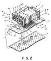
- the connector depicted by 1 in the figure is a so-called angle connector and is coupled and connected to a mating connector (not shown) in a first direction A1 in order to connect a transmission line for transmitting a balanced signal.
- the connector 1 is mounted to a substrate 11, such as a printed board, in a second direction A2 perpendicular to the first direction A1.
- a direction perpendicular to the first and the second directions A1 and A2 will be called a third direction A3.
- the connector 1 comprises an insulator 2 and a number of pairs of conductive signal contacts (signal contact pairs) 3 and 4 held by the insulator 2.
- the signal contact pairs are arranged in parallel to one another at a predetermined pitch in the third direction A3.
- conductive ground contacts 5 are disposed adjacent to and spaced from the signal contact pair.
- Each of the ground contacts 5 extends in the first and the second directions A1 and A2 in a plate-like shape.
- Each ground contact 5 has a flat plate portion 5a press-fitted and fixed to the insulator 2 and a terminal portion 5b protruding from the flat plate portion 5a.
- the ground contacts 5 serve to prevent occurrence of crosstalk between the signal contact pairs.
- the insulator 2 has a coupling portion covered with a shell 6 on upper and lower sides thereof.
- first signal contact 3 one of the signal contacts in each pair will be called a first signal contact 3 and the other will be called a second signal contact 4.
- Each of the first and the second signal contacts 3 and 4 is formed by bending using a press technique and has a generally crank-like shape. Inside the insulator 2, the first signal contact 3 is disposed at a position higher than that of the second signal contact 4 as a whole. The first and the second signal contacts 3 and 4 form an electric pair upon transmission of the balanced signal.
- the first signal contact 3 has a fixed portion 3a press-fitted and fixed to the insulator 2, a contacting portion 3b having elasticity, connected to one end of the fixed portion 3a, and extending forward in the first direction A1, i.e., in a coupling direction, a bent portion 3c connected to the other end of the fixed portion 3a, a first intermediate portion 3d extending from the bent portion 3c rearward in the first direction A1, a second intermediate portion 3e extending from a rear end of the first intermediate portion 3d downward in the second direction A2, and a terminal portion 3f extending from a lower end of the second intermediate portion 3e rearward in the first direction A1 to be soldered to a substrate 11.
- the second signal contact 4 has a fixed portion 4a press-fitted and fixed to the insulator 2, a contacting portion 4b having elasticity, connected to one end of the fixed portion 4a, and extending forward in the first direction A1, i.e., in the coupling direction, a bent portion 4c connected to the other end of the fixed portion 4a, a first intermediate portion 4d extending from the bent portion 4c rearward in the first direction A1, a second intermediate portion 4e extending from a rear end of the first intermediate portion 4d downward in the second direction A2, and a terminal portion 4f extending from a lower end of the second intermediate portion 4e rearward in the first direction A1 to be soldered to the substrate 11.
- the contacting portion 3a of the first signal contact 3 and the contacting portion 4a of the second signal contact 4 are faced to each other with a space left therebetween in the second direction A2.
- the contacting portions 3a and 4a form a socket. Between the contacting portions 3a and 4a, a pin contact of the mating connector is inserted in contact therewith.
- the first intermediate portion 3d of the first signal contact 3 and the first intermediate portion 4d of the second signal contact 4 are displaced or shifted in position from each other in the second direction A2 by a distance X1 and also displaced or shifted in position from each other in the third direction A3.
- the first intermediate portions 3d and 4d are placed at positions which are different from each other in the second and the third directions A2 and A3.
- the second intermediate portion 3e of the first signal contact 3 and the second intermediate portion 4e of the second signal contact 4 are displaced or shifted in position from each other in the first direction A1 by a distance X2 and also displaced or shifted in position from each other in the third direction A3.
- the second intermediate portions 3e and 4e are placed at positions which are different from each other in the first and the third directions A1 and A3.
- the terminal portion 3f of the first signal contact 3 and the terminal portion 4f of the second signal contact 4 are disposed adjacent to each other in the third direction A3.
- the bent portion 3c of the first signal contact 3 and the bent portion 4c of the second signal contact 4 cooperate with each other to make the first and the second signal contacts 3 and 4 be equal in total length to each other. Specifically, by changing the dimensions of the bent portions 3c and 4c of the first and the second signal contacts 3 and 4, the above-mentioned distances X1 and X2 are adjusted. As a result, it is possible to change the degree of electrical coupling between the first and the second signal contacts 3 and 4 and to adjust impedance upon transmission of the balanced signal.
- the substrate 11 has a multilayer micro strip line structure.
- the substrate 11 has a surface 11 a provided with a number of signal pads 12 corresponding to the terminal portions 3f and 4f of the first and the second signal contacts 3 and 4, a number of ground pads 13 connected to the signal pads 12, and a number of ground pads 14 corresponding to the ground contacts 5.
- a ground layer 1t extends in parallel to the surface 11 a.
- the substrate 11 is divided into two parts in a thickness direction.
- the ground layer 15 is formed in a hatched region in the figure.
- the ground layer 15 extends over an area except at least those portions faced to the signal pads 12 in the second direction A2.
- the ground layer 15 is locally removed at the portions located below the signal pads 12.
- the terminal portions 3f and 4f of the signal contacts 3 and 4 are soldered to the signal pads 12 of the substrate 11 by SMT (surface mount technology), respectively.
- the terminal portions 5b of the ground contacts 5 are soldered to the ground pads 13, respectively.
- press punching may form each of the signal contacts.
Landscapes
- Details Of Connecting Devices For Male And Female Coupling (AREA)
- Coupling Device And Connection With Printed Circuit (AREA)
Claims (9)
- Verbinder (1) mit einem Isolator (2) und einem ersten und einem zweiten Signalkontakt (3, 4), die von dem Isolator (2) gehalten sind, wobei jeder des ersten und des zweiten Signalkontaktes (3, 4) aufweist:einen festen Abschnitt (3a, 4a), der an dem Isolator (2) befestigt ist, einen kontaktierenden Abschnitt (3b, 4b), der mit einem Ende des festen Abschnittes (3a, 4a) verbunden ist undsich in einer ersten Richtung (A1) erstreckt;einen gebogenen Abschnitt (3c, 4c), der mit dem anderen Ende des festen Abschnittes (3a, 4a) verbunden ist;einen ersten mittleren Abschnitt (3d, 4d), der sich von dem gebogenen Abschnitt (3c, 4c) in der ersten Richtung (A1) erstreckt;einen zweiten mittleren Abschnitt (3e, 4e), der sich von dem ersten mittleren Abschnitt (3d, 4d) in einer Richtung (A2) senkrecht zu der ersten Richtung (A1) erstreckt; undeinen Anschlußabschnitt (3f, 4f), der sich von dem zweiten mittleren Abschnitt (3e, 4e) in der ersten Richtung (A1) erstreckt, wobei der erste mittlere Abschnitt (3d) des ersten Signalkontaktes (3) und der erste mittlere Abschnitt (4d) des zweiten Signalkontaktes (4) an Positionen angeordnet sind, die sich voneinander in der zweiten Richtung (A2) unterscheiden, der zweite mittlere Abschnitt (3e) des ersten Signalkontaktes (3) und der zweite mittlere Abschnitt (4e) des zweiten Signalkontaktes (4) sich voneinander in der ersten Richtung (A1) unterscheiden, die gebogenen Abschnitte (3c, 4c) so geformt sind, daß der erste und der zweite Signalkontakt im Wesentlichen gleich zueinander in der Gesamtlänge gemacht sind.
- Verbinder nach Anspruch 1, bei dem der erste mittlere Abschnitt (3d) des ersten Signalkontaktes (3) und der zweite mittlere Abschnitt (4d) des zweiten Signalkontaktes (4) an Positionen angeordnet sind, die sich von voneinander in einer dritten Richtung (A3) senkrecht zu der ersten und der zweiten Richtung (A1, A2) unterscheiden.
- Verbinder nach Anspruch 1 oder 2, bei dem der zweite mittlere Abschnitt (3e) des ersten Signalkontaktes (3) und der zweite mittlere Abschnitt (4e) des zweiten Signalkontaktes (4) an Positionen angeordnet sind, die sich voneinander in einer dritten Richtung (A3) senkrecht zu der ersten und zweiten Richtung (A1, A2) unterscheiden.
- Verbinder nach einem der Ansprüche 1 bis 3, bei dem der kontaktierende Abschnitt (3b) des ersten Signalkontaktes (3) und der kontaktierende Abschnitt (4b) des zweiten Signalkontaktes (4) einander in der zweiten Richtung (A2) zugewandt sind.
- Verbinder nach einem der Ansprüche 1 bis 4, bei dem der Anschlußabschnitt (3f) des ersten Signalkontaktes (3) und der Anschlußabschnitt (4f) des zweiten Signalkontaktes (4) benachbart zueinander in einer dritten Richtung (A3) senkrecht zu der ersten und der zweiten Richtung (A1, A2) vorgesehen sind.
- Verbinder nach einem der Ansprüche 1 bis 5, weiter mit einem ersten Massekontakt (5), der von dem Isolator (2) gehalten ist, wobei eine Kombination des ersten und des zweiten Signalkontaktes (3, 4) ein Kontaktpaar bildet, der erste Massekontakt (5) benachbart zu dem Kontaktpaar auf einer Seite des Kontaktpaares in einer dritten Richtung (A3) senkrecht zu der ersten und der zweiten Richtung (A1, A2) vorgesehen ist, bevorzugt der erste Massekontakt (5) sich in der ersten und in der zweiten Richtung (A1, A2) in einer plattenartigen Form erstreckt.
- Verbinder nach einem der Ansprüche 1 bis 6, mit einem zweiten Massekontakt (5), der von dem Isolator (2) gehalten ist und benachbart zu dem Kontaktpaar auf der anderen Seite des Kontaktpaares in der dritten Richtung (A3) vorgesehen ist, bevorzugt der zweite Massekontakt (5) sich in der ersten und in der zweiten Richtung (A1, A2) in einer plattenartigen Form erstreckt.
- Verbinder nach einem der Ansprüche 1 bis 7, bei dem der erste und der zweite Massekontakt (5) zum Übertragen eines ausgeglichenen Signales benutzt sind.
- Kombination eines Substrates (11) und des Verbinders (1) nach einem der Ansprüche 1 bis 8, wobei das Substrat (11) aufweist:einen Plattenabschnitt;erste und zweite Signalanschlußflecken (12), die auf einer Oberfläche des Plattenabschnittes vorgesehen sind und ausgelegt sind zum Verbinden mit den Anschlußabschnitten (3f, 4f) des ersten und des zweiten Signalkontaktes (3, 4); undeine Masseschicht (5), die innerhalb des Plattenabschnittes gebildet ist und sich parallel zu der Oberfläche (11a) des Plattenabschnittes über ein Gebiet erstreckt mit Ausnahme von mindestens jenen Abschnitten, die den ersten und den zweiten Signalanschlußflecken (12) in der zweiten Richtung (A2) zugewandt sind.
Applications Claiming Priority (2)
| Application Number | Priority Date | Filing Date | Title |
|---|---|---|---|
| JP2003111567A JP2004319257A (ja) | 2003-04-16 | 2003-04-16 | 平衡伝送用コネクタ |
| JP2003111567 | 2003-04-16 |
Publications (3)
| Publication Number | Publication Date |
|---|---|
| EP1469558A2 EP1469558A2 (de) | 2004-10-20 |
| EP1469558A3 EP1469558A3 (de) | 2004-12-29 |
| EP1469558B1 true EP1469558B1 (de) | 2006-09-06 |
Family
ID=32906038
Family Applications (1)
| Application Number | Title | Priority Date | Filing Date |
|---|---|---|---|
| EP04009025A Expired - Lifetime EP1469558B1 (de) | 2003-04-16 | 2004-04-15 | Verbinder geeignet zur symmetrischen Signalübertragung und Substrat zur Montage |
Country Status (6)
| Country | Link |
|---|---|
| US (1) | US6974336B2 (de) |
| EP (1) | EP1469558B1 (de) |
| JP (1) | JP2004319257A (de) |
| CN (1) | CN1279661C (de) |
| DE (1) | DE602004002229T2 (de) |
| TW (1) | TWI276262B (de) |
Families Citing this family (6)
| Publication number | Priority date | Publication date | Assignee | Title |
|---|---|---|---|---|
| CN2932689Y (zh) | 2006-04-10 | 2007-08-08 | 富士康(昆山)电脑接插件有限公司 | 电连接器 |
| JP5054462B2 (ja) * | 2007-08-06 | 2012-10-24 | 富士通コンポーネント株式会社 | 平衡伝送用コネクタ |
| JP4839362B2 (ja) * | 2008-11-14 | 2011-12-21 | ホシデン株式会社 | 高周波回路モジュール |
| JP4887393B2 (ja) * | 2009-03-24 | 2012-02-29 | ホシデン株式会社 | コネクタ |
| JP6215125B2 (ja) * | 2014-04-21 | 2017-10-18 | 日本航空電子工業株式会社 | コネクタ |
| JP7244412B2 (ja) * | 2019-12-25 | 2023-03-22 | 京セラ株式会社 | コネクタ及び電子機器 |
Family Cites Families (12)
| Publication number | Priority date | Publication date | Assignee | Title |
|---|---|---|---|---|
| US5085601A (en) * | 1990-12-11 | 1992-02-04 | Amp Incorporated | Reduced insertion force electrical connector |
| US5244412A (en) * | 1991-12-24 | 1993-09-14 | Stewart Connector Systems, Inc. | Electrical device for surface mounting on a circuit board and mounting component thereof |
| JP3108239B2 (ja) | 1993-02-19 | 2000-11-13 | 富士通株式会社 | インピーダンス整合型電気コネクタ |
| JPH0785931A (ja) * | 1993-09-17 | 1995-03-31 | Kel Corp | 電気コネクタ |
| JP2715910B2 (ja) | 1994-06-27 | 1998-02-18 | 日本電気株式会社 | 多層印刷配線板及びその製造方法 |
| JP3232225B2 (ja) * | 1995-11-15 | 2001-11-26 | ヒロセ電機株式会社 | 情報カード、並びにそのためのバックコネクタ及びカードブランク |
| US5795191A (en) * | 1996-09-11 | 1998-08-18 | Preputnick; George | Connector assembly with shielded modules and method of making same |
| US6503103B1 (en) * | 1997-02-07 | 2003-01-07 | Teradyne, Inc. | Differential signal electrical connectors |
| JP3238895B2 (ja) * | 1997-08-28 | 2001-12-17 | ヒロセ電機株式会社 | モジュラージャック |
| US5919063A (en) * | 1997-09-17 | 1999-07-06 | Berg Technology, Inc. | Three row plug and receptacle connectors with ground shield |
| JP2000068007A (ja) | 1998-08-20 | 2000-03-03 | Fujitsu Takamisawa Component Ltd | ケーブル付き平衡伝送用コネクタ |
| JP2000068006A (ja) * | 1998-08-20 | 2000-03-03 | Fujitsu Takamisawa Component Ltd | ライトアングル型コネクタ |
-
2003
- 2003-04-16 JP JP2003111567A patent/JP2004319257A/ja active Pending
-
2004
- 2004-03-30 CN CNB2004100318186A patent/CN1279661C/zh not_active Expired - Fee Related
- 2004-04-13 US US10/823,025 patent/US6974336B2/en not_active Expired - Fee Related
- 2004-04-15 TW TW093110449A patent/TWI276262B/zh not_active IP Right Cessation
- 2004-04-15 DE DE602004002229T patent/DE602004002229T2/de not_active Expired - Fee Related
- 2004-04-15 EP EP04009025A patent/EP1469558B1/de not_active Expired - Lifetime
Also Published As
| Publication number | Publication date |
|---|---|
| DE602004002229T2 (de) | 2007-07-19 |
| TW200428718A (en) | 2004-12-16 |
| CN1538578A (zh) | 2004-10-20 |
| CN1279661C (zh) | 2006-10-11 |
| TWI276262B (en) | 2007-03-11 |
| EP1469558A3 (de) | 2004-12-29 |
| DE602004002229D1 (de) | 2006-10-19 |
| US6974336B2 (en) | 2005-12-13 |
| US20040209496A1 (en) | 2004-10-21 |
| JP2004319257A (ja) | 2004-11-11 |
| EP1469558A2 (de) | 2004-10-20 |
Similar Documents
| Publication | Publication Date | Title |
|---|---|---|
| US7052320B2 (en) | Electrical connector having shielding plates | |
| US7549882B2 (en) | Connector capable of absorbing an error in mounting position | |
| US7310875B2 (en) | Connector for high-speed communications | |
| US7172434B2 (en) | Electrical connection apparatus capable of resisting repetition of connection and disconnection | |
| US7435110B2 (en) | Electrical connector with improved contact arrangement | |
| US7604510B2 (en) | High speed transmission connector | |
| US6592407B2 (en) | High-speed card edge connector | |
| EP1511124A2 (de) | Elektrischeverbinder mit verbesserter Leistung | |
| EP1453152B1 (de) | Steckverbinder, bei dem das Übersprechen durch einen Erdungskontakt unterdrückt wird | |
| EP1104049A1 (de) | Flexibler Verbinder mit eingebauten übertragungslinien | |
| JP3762730B2 (ja) | コネクタ | |
| US6817868B2 (en) | Intermediate board electrical connector | |
| EP1469558B1 (de) | Verbinder geeignet zur symmetrischen Signalübertragung und Substrat zur Montage | |
| US7004763B2 (en) | Board-to-board electrical connector assembly | |
| US6663445B1 (en) | Electrical connector with staggered contacts | |
| US12388221B2 (en) | Electrical connector structure | |
| US7445470B2 (en) | Electrical connector with improved housing | |
| US20240388024A1 (en) | Board connector and board-to-board connector | |
| US7413475B2 (en) | Electrical connector having ground planes | |
| US20240322472A1 (en) | Electrical connector and conductive terminal thereof | |
| CN223809266U (zh) | 信号端子和电连接器 | |
| EP1063726A2 (de) | Elektrischer Steckverbinder mit mehrfachen Kontakten | |
| US6979237B2 (en) | Electrical connector having receptacle contacts | |
| CN210111110U (zh) | 电连接器 | |
| WO2004057705A1 (ja) | 電気コネクタ |
Legal Events
| Date | Code | Title | Description |
|---|---|---|---|
| PUAI | Public reference made under article 153(3) epc to a published international application that has entered the european phase |
Free format text: ORIGINAL CODE: 0009012 |
|
| AK | Designated contracting states |
Kind code of ref document: A2 Designated state(s): AT BE BG CH CY CZ DE DK EE ES FI FR GB GR HU IE IT LI LU MC NL PL PT RO SE SI SK TR |
|
| AX | Request for extension of the european patent |
Extension state: AL HR LT LV MK |
|
| 17P | Request for examination filed |
Effective date: 20040910 |
|
| PUAL | Search report despatched |
Free format text: ORIGINAL CODE: 0009013 |
|
| AK | Designated contracting states |
Kind code of ref document: A3 Designated state(s): AT BE BG CH CY CZ DE DK EE ES FI FR GB GR HU IE IT LI LU MC NL PL PT RO SE SI SK TR |
|
| AX | Request for extension of the european patent |
Extension state: AL HR LT LV MK |
|
| AKX | Designation fees paid |
Designated state(s): DE FR GB |
|
| GRAP | Despatch of communication of intention to grant a patent |
Free format text: ORIGINAL CODE: EPIDOSNIGR1 |
|
| GRAS | Grant fee paid |
Free format text: ORIGINAL CODE: EPIDOSNIGR3 |
|
| GRAA | (expected) grant |
Free format text: ORIGINAL CODE: 0009210 |
|
| AK | Designated contracting states |
Kind code of ref document: B1 Designated state(s): DE FR GB |
|
| REG | Reference to a national code |
Ref country code: GB Ref legal event code: FG4D |
|
| REF | Corresponds to: |
Ref document number: 602004002229 Country of ref document: DE Date of ref document: 20061019 Kind code of ref document: P |
|
| ET | Fr: translation filed | ||
| PLBE | No opposition filed within time limit |
Free format text: ORIGINAL CODE: 0009261 |
|
| STAA | Information on the status of an ep patent application or granted ep patent |
Free format text: STATUS: NO OPPOSITION FILED WITHIN TIME LIMIT |
|
| 26N | No opposition filed |
Effective date: 20070607 |
|
| PGFP | Annual fee paid to national office [announced via postgrant information from national office to epo] |
Ref country code: DE Payment date: 20080430 Year of fee payment: 5 |
|
| GBPC | Gb: european patent ceased through non-payment of renewal fee |
Effective date: 20080415 |
|
| PG25 | Lapsed in a contracting state [announced via postgrant information from national office to epo] |
Ref country code: GB Free format text: LAPSE BECAUSE OF NON-PAYMENT OF DUE FEES Effective date: 20080415 |
|
| REG | Reference to a national code |
Ref country code: FR Ref legal event code: ST Effective date: 20091231 |
|
| PG25 | Lapsed in a contracting state [announced via postgrant information from national office to epo] |
Ref country code: DE Free format text: LAPSE BECAUSE OF NON-PAYMENT OF DUE FEES Effective date: 20091103 |
|
| PG25 | Lapsed in a contracting state [announced via postgrant information from national office to epo] |
Ref country code: FR Free format text: LAPSE BECAUSE OF NON-PAYMENT OF DUE FEES Effective date: 20091222 |
|
| PGFP | Annual fee paid to national office [announced via postgrant information from national office to epo] |
Ref country code: FR Payment date: 20080428 Year of fee payment: 5 |