EP1475471A1 - Capteur de turbidité avec caractéristiques de transmission adaptées et procédé pour fabriquer celui-ci - Google Patents
Capteur de turbidité avec caractéristiques de transmission adaptées et procédé pour fabriquer celui-ci Download PDFInfo
- Publication number
- EP1475471A1 EP1475471A1 EP04015976A EP04015976A EP1475471A1 EP 1475471 A1 EP1475471 A1 EP 1475471A1 EP 04015976 A EP04015976 A EP 04015976A EP 04015976 A EP04015976 A EP 04015976A EP 1475471 A1 EP1475471 A1 EP 1475471A1
- Authority
- EP
- European Patent Office
- Prior art keywords
- transmitter
- receiver
- radiation
- turbidity sensor
- wavelength
- Prior art date
- Legal status (The legal status is an assumption and is not a legal conclusion. Google has not performed a legal analysis and makes no representation as to the accuracy of the status listed.)
- Granted
Links
Images


Classifications
-
- G—PHYSICS
- G01—MEASURING; TESTING
- G01N—INVESTIGATING OR ANALYSING MATERIALS BY DETERMINING THEIR CHEMICAL OR PHYSICAL PROPERTIES
- G01N15/00—Investigating characteristics of particles; Investigating permeability, pore-volume or surface-area of porous materials
- G01N15/06—Investigating concentration of particle suspensions
-
- A—HUMAN NECESSITIES
- A47—FURNITURE; DOMESTIC ARTICLES OR APPLIANCES; COFFEE MILLS; SPICE MILLS; SUCTION CLEANERS IN GENERAL
- A47L—DOMESTIC WASHING OR CLEANING; SUCTION CLEANERS IN GENERAL
- A47L15/00—Washing or rinsing machines for crockery or tableware
- A47L15/42—Details
- A47L15/4297—Arrangements for detecting or measuring the condition of the washing water, e.g. turbidity
-
- D—TEXTILES; PAPER
- D06—TREATMENT OF TEXTILES OR THE LIKE; LAUNDERING; FLEXIBLE MATERIALS NOT OTHERWISE PROVIDED FOR
- D06F—LAUNDERING, DRYING, IRONING, PRESSING OR FOLDING TEXTILE ARTICLES
- D06F34/00—Details of control systems for washing machines, washer-dryers or laundry dryers
- D06F34/14—Arrangements for detecting or measuring specific parameters
- D06F34/22—Condition of the washing liquid, e.g. turbidity
-
- G—PHYSICS
- G01—MEASURING; TESTING
- G01N—INVESTIGATING OR ANALYSING MATERIALS BY DETERMINING THEIR CHEMICAL OR PHYSICAL PROPERTIES
- G01N21/00—Investigating or analysing materials by the use of optical means, i.e. using sub-millimetre waves, infrared, visible or ultraviolet light
- G01N21/17—Systems in which incident light is modified in accordance with the properties of the material investigated
- G01N21/47—Scattering, i.e. diffuse reflection
- G01N21/49—Scattering, i.e. diffuse reflection within a body or fluid
-
- G—PHYSICS
- G01—MEASURING; TESTING
- G01N—INVESTIGATING OR ANALYSING MATERIALS BY DETERMINING THEIR CHEMICAL OR PHYSICAL PROPERTIES
- G01N21/00—Investigating or analysing materials by the use of optical means, i.e. using sub-millimetre waves, infrared, visible or ultraviolet light
- G01N21/17—Systems in which incident light is modified in accordance with the properties of the material investigated
- G01N21/47—Scattering, i.e. diffuse reflection
- G01N21/49—Scattering, i.e. diffuse reflection within a body or fluid
- G01N21/53—Scattering, i.e. diffuse reflection within a body or fluid within a flowing fluid, e.g. smoke
- G01N21/534—Scattering, i.e. diffuse reflection within a body or fluid within a flowing fluid, e.g. smoke by measuring transmission alone, i.e. determining opacity
-
- D—TEXTILES; PAPER
- D06—TREATMENT OF TEXTILES OR THE LIKE; LAUNDERING; FLEXIBLE MATERIALS NOT OTHERWISE PROVIDED FOR
- D06F—LAUNDERING, DRYING, IRONING, PRESSING OR FOLDING TEXTILE ARTICLES
- D06F2103/00—Parameters monitored or detected for the control of domestic laundry washing machines, washer-dryers or laundry dryers
- D06F2103/20—Washing liquid condition, e.g. turbidity
-
- D—TEXTILES; PAPER
- D06—TREATMENT OF TEXTILES OR THE LIKE; LAUNDERING; FLEXIBLE MATERIALS NOT OTHERWISE PROVIDED FOR
- D06F—LAUNDERING, DRYING, IRONING, PRESSING OR FOLDING TEXTILE ARTICLES
- D06F2103/00—Parameters monitored or detected for the control of domestic laundry washing machines, washer-dryers or laundry dryers
- D06F2103/64—Radiation, e.g. microwaves
Definitions
- the present invention relates generally to turbidity sensors for household appliances, such as. Dishwashers, washing machines and dryers.
- the present concerns Invention turbidity sensors in which the transmission characteristics of individual components, such as. of a transmitter and a receiver for optical radiation, one on top of the other are or will be coordinated.
- Turbidity sensors generally consist of a transmitter and a receiver for optical Radiation that spreads through the medium used. Interactions of Radiation on its path of propagation through the medium are used to target the Close turbidity or contamination of the medium.
- the turbidity sensors have a housing that is arranged in a household appliance is that at least the areas of the housing that have the transmitter and receiver extend into the interior of the device in order to prevent the radiation from operating To direct the device inside the medium.
- turbidity sensors are essential for their operation, because it is the accuracy and reliability of turbidity or contamination detection certainly.
- For an undamped transmission path between a transmitter and one Receiver of a turbidity sensor results in the receiver current generated by the receiver from a multiplication of that supplied to the transmitter for generating the radiation Stroms with a constant, which in addition to the sizes mentioned below also by the Areas of the sensor housing and the medium through which the measuring beam is affected spreads.
- the constant on the transmitter side depends on the efficiency of the transmitter, for example that Efficiency of a transmitter diode for optical radiation or the quality of one used with it Transmitter chip. Accordingly, the constant on the receiver side depends on the efficiency of the Receiver influenced, for example by the quality of a receiver chip used.
- turbidity sensors To optimize the transmission characteristics of turbidity sensors, i.e. for a given Voltage or a predetermined current for operating the transmitter on the receiver side the highest possible output voltage or the highest possible output current to get, are usually selected components to build the transmitter and Receiver used. For this, it is known to transmit and receive or their components before setting up a turbidity sensor with regard to its transmission or reception characteristics to be measured and then grouped accordingly, i.e. matching Transmitter and receiver to be used in pairs in the turbidity sensors. This approach is time-consuming due to the need to check the transmitter and receiver and costly and generally leads to only certain groups of transmitter and receiver pairs can be used.
- EP 0 178 031 A1 discloses a turbidity sensor for household appliances with two transmitters and a recipient.
- the object of the present invention is generally the above-mentioned problems of Eliminate prior art.
- the present invention is intended to be a method provide for the production of turbidity sensors, which makes it possible, on the one hand, at Use of very high quality transmitters and receivers whose higher absolute values are simple Way to compensate and on the other hand the use of less precise or poorly on each other to enable selected ("inappropriate") transmitters and receivers.
- turbidity sensors with transmission characteristics provide that compensate for the dispersion of high quality transmitters and receivers or effects resulting from a combination of inaccurate transmitter and inaccurate receiver compensate.
- the present invention provides a method according to claim 1 for setting output voltages of a turbidity sensor and one accordingly constructed turbidity sensor according to claim 5 ready.
- the turbidity by means of two radiations of different wavelengths of a medium is determined depending on which wavelength the receiver of the turbidity sensor, whose ohmic load on the output side is set such that regardless of the wavelength of the received radiation, essentially result in the same output voltages.
- FIGS. 1 to 5 taken that relate to the invention of the underlying parent application.
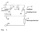
- a turbidity sensor (not designated) includes one Transmitter 2, which emits an optical beam 4.
- the optical beam 4 is from one Receiver 6 received, depending on the received radiation intensity Receiver current generated.
- the radiation intensity output by the transmitter 2 become the radiation intensity received by the receiver 6
- the transmitter 2 comprises a transmitter diode 10 connected to a potential 8, the output side is connected to a transmitter potential 12.
- Der Receiver 6 has a receiver transistor 14, which is also connected to potential 8 is. So far, the circuit arrangement corresponds to conventional circuit arrangements of transmitters and receivers of turbidity sensors.
- the receiver transistor 14 has a receiver potential on the output side 16 connected, which, like the transmitter potential 12, by control electronics (not shown) is defined. That is, the transmitter diode 10 and the receiver transistor 14 are each connected to corresponding connections of control electronics. This arrangement is indicated in Fig. 1 by the dashed lines.
- the receiver 6, more precisely its receiver transistor 14, on the output side with an advantageously integrated structural, Load resistor 18 connected, which in turn is connected to a receiver potential 20 is.
- the potential 8 is usually connected to a positive supply voltage, whereas the transmitter potential 12 and the receiver potential 16 with the controller and that Potential 20 are each connected to a reference potential of 0 volts.
- the potentials 12 and 16 are inputs or control lines and the potential 20 is used for one for operation of the turbidity sensor control used as a reference potential, with a supply potential the controller is used as the mass for the turbidity sensor.
- the radiation power generated by the transmitter diode 10 is directly proportional to that by the transmitter diode 10 flowing transmitter current, as long as the transmitter diode 10 in the linear range is operated. This proportional ratio does not exist if the transmitter diode 10 is operated outside of its linear range, i.e. the transmitter current is small. Accordingly a transmitter current is to be used to operate the transmitter diode 10, which is an operation ensures the transmitter diode 10 in its linear range.
- the radiation intensity of the Beam 4 be so large that the receiver transistor 14 operates in its linear region is a proportionality between the received radiation intensity and the generated To reach the receiver current.
- variable R of the load resistor 18 is varied as a function of the actual transmission characteristic. In this way, higher transmission constants K can be compensated for by lower load resistances R and vice versa.
- the load resistance 18 is dependent on the width and / or the position of the tolerance range set, which is characterized by the respective combination of the individual optical elements, i.e. in particular the transmitter 2 and the receiver 6 and the housing results.
- the one in the sensor housing itself and in particular in the receiver 6, for example on one Circuit board, arranged load resistor 18 can be set in different ways become. It is also planned to use single or multiple trimming resistors, for example, to solder an existing load resistance (e.g. Resistances of connected components, lines, etc.). Can also Laser-trimmed resistors are used and / or resistors designed as potentiometers be used.
- the adaptation of the load resistance 18 is made for the sake of simplicity described with regard to the transmitter 2 and the receiver 6. But this adjustment is also applicable with regard to individual or a plurality of further components of a turbidity sensor.
- the technical quantities determining the transmission property for the beam 4 are not known, the transmitter 2 and the receiver 6 are measured in order to determine a resistance R for the load resistance 18, which ensures the desired output voltage U e ,
- the transmitters and receivers that can be used with turbidity sensors are becoming ever higher quality, ie the absolute values of the optical parameters are always higher.
- the higher-value components still approximate the percentage spread as previous, poorer components. Accordingly, the higher-value components deliver higher absolute values, but in their tolerance ranges, they show percentage fluctuations comparable to poorer components. As stated above, this can result in the receiver 6 supplying a high output current I e .
- small resistors R are generally used for the load resistor 18 in these cases.
- the load resistor 18 serves on the one hand to adapt the transmitter 2 and the receiver 6 to one another, and on the other hand to "improve the technical properties of these components"compensate". In this way, a desired transmission characteristic is achieved by adapting the load resistance 18 as a function of the transmitter 2 and the receiver 6.
- load resistor 18 has transmission characteristics can be achieved with available transmitter and receiver pairings would otherwise not be reachable. This applies, for example, in the event that the reception characteristic a receiver intended for use with a turbidity sensor Prevents use of a desired station. By an appropriate choice of Size of the load resistor 18 can be the intended receiver and the desired one Transmitters can be used in a turbidity sensor, although these are not actually "to each other fit".
- the load resistor 18 enables unavailable power or Realize sensitivity selection groups of transmitter and receiver pairs by the load resistance 18 is set accordingly.
- 2 illustrates the influence of the load resistance 18 on the tolerance range of a turbidity sensor, the influence of the load resistance 18 also being referred to below as a change or shift in tolerance.
- 2 shows the beam intensity P s of the transmitter 2 as a function of the transmitter current I s , transmitter characteristics 1 and 2 indicating transmitters of different qualities (transmitter characteristic 1: poor transmitter; transmitter characteristic 2: good transmitter).
- the receiver current I e of the receiver 6 as a function of the received beam intensity (irradiation intensity) P e for a receiver of a quality is shown in FIG. 2 on the right.
- the receiver 6 receives radiation with a radiation sensitivity P e1 for the bad transmitter and a radiation sensitivity P e2 for the good transmitter. Based on the receiver characteristic, a receiver current I e1 results in response to the radiation received by the bad transmitter, while a receiver current I e2 results from the radiation originating from the good transmitter.
- the output voltage U e that results as a function of the receiver current I e is shown in FIG. 2 at the bottom right for a load resistor 18 with the resistance value R2 and a load resistor 18 with the higher resistance value R1.
- An output voltage U e12 results for the resistance value R2 for the receiver current I e1
- the receiver current I e2 produces an output voltage U e22 .
- output voltages U e11 and U e21 result for the receiver currents I e1 and I e2 .
- the resistance value R1 for the load resistor 18 is selected accordingly for the bad transmitter (transmitter characteristic 1) or the resulting receiver current I e1 .
- the resistance value R2 for the load resistor 18 is set in order to achieve the same output voltages in both cases, namely U e11 and U e22 .
- the characteristic curve A represents a good transmitter-receiver pairing, while the characteristic curves B, C and D show increasingly poorer transmitter-receiver pairs. It is assumed here that the load resistance 18 has a value of 10 kOhm.
- FIG. 4 shows a tolerance change or shift when using a Load resistance 18 with a value of 5 kOhm, here a characteristic curve A ' good and the characteristics B ', C' and D 'increasingly poor transmitter-receiver pairings specify.
- the range of the output voltages of the receiver 6 can be reached in the Characteristic curves for transmitter-receiver pairings are shifted.
- the Area in which the output voltage of the receiver 6 lies for the transmitter-receiver pairings with the characteristics A / A 'and C / C' if for the transmitter-receiver pairing with the characteristic curves A / A ', the load resistance 18 has a value of 5 kOhm has a load resistance for the transmitter-receiver pairing with the characteristic curves C / C ' 18 with a value of 10 kOhm is selected.
- turbidity sensors with two transmitters, emit radiation of different wavelengths, and a receiver that is provided for receiving both radiations.
- Turbidity sensor in addition to the components shown in Fig. 1, another transmitter 28 with one connected between the potential 8 and a second transmitter potential 30 Transmitter diode 32.
- the transmitter diode 32 emits radiation 34, the wavelength of which differs from that of radiation 4.
- the use of different radiations Wavelength can be used to indicate turbidity or contamination of a medium due to different causes (e.g. material particles, contaminants, gas bubbles, etc.) to distinguish.
- the transmitter 2 and the transmitter 24 alternate activated so that the receiver 6 receives the radiation 4 and 34 alternately.
- the spectral sensitivity of the receiver 6 is predetermined for the reception of radiation of a certain wavelength, different output voltages U e result when radiation that has approximately the same intensity but has different wavelengths is received.
- the receiver 6 silicon-based components with a spectral sensitivity designed for wavelengths in the range of 900 nm, a transmitter 2 for emitting infrared radiation with a wavelength of approximately 880 nm and a transmitter 28 for emitting radiation with a wavelength of approximately 560 nm (green light), the sensitivity of the receiver 6 is approximately halved for wavelengths of approximately 560 nm compared to wavelengths of approximately 880 nm. Accordingly, when infrared radiation is received, the output voltage U e is approximately twice that of reception Radiation with a wavelength of approximately 560 nm if both radiations have approximately the same intensity.
- the load resistance 18 is varied depending on the wavelength of the received radiation.
- the load resistor 18 determines a first resistance value for adaptation to the transmitter 2 and a second resistance value for adaptation to the transmitter 28. 6, the load resistance 18 is set to the first resistance value when the radiation 4 is transmitted or received and to the second resistance value when the radiation 34 is transmitted or received. In this way, approximately equal output voltages U e are generated regardless of the wavelength of the received radiation.
- For switching the load resistor 18 between the first and second resistance values is one, e.g. electronic circuit integrated in the turbidity sensor, where control signals for the transmitters 2 and 28 as control signals for switching of the load resistor 18 can be used.
Landscapes
- Chemical & Material Sciences (AREA)
- General Health & Medical Sciences (AREA)
- Life Sciences & Earth Sciences (AREA)
- Health & Medical Sciences (AREA)
- Analytical Chemistry (AREA)
- Biochemistry (AREA)
- Physics & Mathematics (AREA)
- General Physics & Mathematics (AREA)
- Immunology (AREA)
- Pathology (AREA)
- Engineering & Computer Science (AREA)
- Textile Engineering (AREA)
- Dispersion Chemistry (AREA)
- Investigating Or Analysing Materials By Optical Means (AREA)
Applications Claiming Priority (1)
| Application Number | Priority Date | Filing Date | Title |
|---|---|---|---|
| EP02003147A EP1338693B1 (fr) | 2002-02-14 | 2002-02-14 | Capteur de turbidité avec caractéristiques de transmission adaptées et procédé pour fabriquer celui-ci |
Related Parent Applications (1)
| Application Number | Title | Priority Date | Filing Date |
|---|---|---|---|
| EP02003147A Division EP1338693B1 (fr) | 2002-02-14 | 2002-02-14 | Capteur de turbidité avec caractéristiques de transmission adaptées et procédé pour fabriquer celui-ci |
Publications (2)
| Publication Number | Publication Date |
|---|---|
| EP1475471A1 true EP1475471A1 (fr) | 2004-11-10 |
| EP1475471B1 EP1475471B1 (fr) | 2006-09-27 |
Family
ID=27635790
Family Applications (2)
| Application Number | Title | Priority Date | Filing Date |
|---|---|---|---|
| EP04015976A Expired - Lifetime EP1475471B1 (fr) | 2002-02-14 | 2002-02-14 | Capteur de turbidité avec caractéristiques de transmission adaptées et procédé pour fabriquer celui-ci |
| EP02003147A Expired - Lifetime EP1338693B1 (fr) | 2002-02-14 | 2002-02-14 | Capteur de turbidité avec caractéristiques de transmission adaptées et procédé pour fabriquer celui-ci |
Family Applications After (1)
| Application Number | Title | Priority Date | Filing Date |
|---|---|---|---|
| EP02003147A Expired - Lifetime EP1338693B1 (fr) | 2002-02-14 | 2002-02-14 | Capteur de turbidité avec caractéristiques de transmission adaptées et procédé pour fabriquer celui-ci |
Country Status (4)
| Country | Link |
|---|---|
| US (1) | US6833555B2 (fr) |
| EP (2) | EP1475471B1 (fr) |
| KR (1) | KR100991604B1 (fr) |
| DE (2) | DE50208292D1 (fr) |
Cited By (1)
| Publication number | Priority date | Publication date | Assignee | Title |
|---|---|---|---|---|
| EP2182105A1 (fr) * | 2008-11-04 | 2010-05-05 | Electrolux Home Products Corporation N.V. | Capteur de turbidité |
Families Citing this family (8)
| Publication number | Priority date | Publication date | Assignee | Title |
|---|---|---|---|---|
| US20060055927A1 (en) * | 2004-09-16 | 2006-03-16 | Rosemount Analytical Inc. | Turbidity sensor |
| US20060061765A1 (en) * | 2004-09-16 | 2006-03-23 | Behzad Rezvani | Turbidity sensor with improved noise rejection |
| US9575087B2 (en) | 2012-09-06 | 2017-02-21 | Parker-Hannifin Corporation | Risk-managed, single-use, pre-calibrated, pre-sterilized sensors for use in bio-processing applications |
| DE102007031480B4 (de) * | 2007-07-06 | 2009-05-14 | BSH Bosch und Siemens Hausgeräte GmbH | Sensoreinrichtung und Verfahren zur Erfassung der Trübung von Spülflotte |
| DE102010054447A1 (de) | 2010-12-14 | 2012-06-14 | Emz-Hanauer Gmbh & Co. Kgaa | Optischer Sensor zum Einbau in eine Waschmaschine oder Geschirrspülmaschine |
| US8817259B2 (en) | 2011-03-25 | 2014-08-26 | Parker-Hannifin Corporation | Optical sensors for monitoring biopharmaceutical solutions in single-use containers |
| JP5360180B2 (ja) * | 2011-10-12 | 2013-12-04 | パナソニック株式会社 | 食器洗い機 |
| CN109323360B (zh) * | 2018-06-29 | 2021-06-01 | 爱源(厦门)电子有限公司 | 一种空气质量检测方法和具有自动校准功能的空气净化器 |
Citations (2)
| Publication number | Priority date | Publication date | Assignee | Title |
|---|---|---|---|---|
| US3449578A (en) * | 1966-04-12 | 1969-06-10 | Honeywell Inc | Turbidimeter using photoelectric linearizing circuit including switching circuit to insert preselected resistances |
| US4257708A (en) * | 1978-04-28 | 1981-03-24 | Tokyo Shibaura Denki Kabushiki Kaisha | Apparatus for measuring the degree of rinsing |
Family Cites Families (3)
| Publication number | Priority date | Publication date | Assignee | Title |
|---|---|---|---|---|
| US4155653A (en) * | 1977-10-14 | 1979-05-22 | The United States Of America As Represented By The Secretary Of The Navy | Smoke-measuring transducer |
| WO1983000228A1 (fr) * | 1981-07-11 | 1983-01-20 | Siegfried Jochimsen | Appareil pour la mesure du temps de coagulation du sang et procede pour saisir et mesurer le temps |
| DE19521326A1 (de) | 1995-06-12 | 1996-12-19 | Bosch Siemens Hausgeraete | Verfahren zur Temperaturkompensation der Meßwerte eines Trübungssensors in einer automatischen Wasch- oder Geschirrspülmaschine |
-
2002
- 2002-02-14 EP EP04015976A patent/EP1475471B1/fr not_active Expired - Lifetime
- 2002-02-14 EP EP02003147A patent/EP1338693B1/fr not_active Expired - Lifetime
- 2002-02-14 DE DE50208292T patent/DE50208292D1/de not_active Expired - Lifetime
- 2002-02-14 DE DE50204937T patent/DE50204937D1/de not_active Expired - Lifetime
-
2003
- 2003-02-13 KR KR1020030008970A patent/KR100991604B1/ko not_active Expired - Fee Related
- 2003-02-13 US US10/366,098 patent/US6833555B2/en not_active Expired - Lifetime
Patent Citations (2)
| Publication number | Priority date | Publication date | Assignee | Title |
|---|---|---|---|---|
| US3449578A (en) * | 1966-04-12 | 1969-06-10 | Honeywell Inc | Turbidimeter using photoelectric linearizing circuit including switching circuit to insert preselected resistances |
| US4257708A (en) * | 1978-04-28 | 1981-03-24 | Tokyo Shibaura Denki Kabushiki Kaisha | Apparatus for measuring the degree of rinsing |
Cited By (6)
| Publication number | Priority date | Publication date | Assignee | Title |
|---|---|---|---|---|
| EP2182105A1 (fr) * | 2008-11-04 | 2010-05-05 | Electrolux Home Products Corporation N.V. | Capteur de turbidité |
| WO2010051906A1 (fr) * | 2008-11-04 | 2010-05-14 | Electrolux Home Products Corporation N.V. | Détecteur de turbidité |
| KR20110086717A (ko) * | 2008-11-04 | 2011-07-29 | 일렉트로룩스 홈 프로덕츠 코오포레이션 엔.브이. | 탁도 센서 |
| CN102224288B (zh) * | 2008-11-04 | 2013-06-12 | 伊莱克斯家用产品公司 | 浑浊度传感器 |
| US8767213B2 (en) | 2008-11-04 | 2014-07-01 | Electrolux Home Products Corporation, N.V. | Dishwasher |
| KR101724165B1 (ko) | 2008-11-04 | 2017-04-06 | 일렉트로룩스 홈 프로덕츠 코오포레이션 엔.브이. | 탁도 센서 |
Also Published As
| Publication number | Publication date |
|---|---|
| DE50208292D1 (de) | 2006-11-09 |
| EP1338693B1 (fr) | 2005-11-16 |
| EP1475471B1 (fr) | 2006-09-27 |
| DE50204937D1 (de) | 2005-12-22 |
| EP1338693A1 (fr) | 2003-08-27 |
| KR20030068456A (ko) | 2003-08-21 |
| US20030173530A1 (en) | 2003-09-18 |
| US6833555B2 (en) | 2004-12-21 |
| KR100991604B1 (ko) | 2010-11-04 |
Similar Documents
| Publication | Publication Date | Title |
|---|---|---|
| EP3124992B1 (fr) | Récepteur de lumière ayant des photodiodes à avalanche en mode geiger et procédé de lecture | |
| DE19723645B4 (de) | Anordnung zur Signalübertragung zwischen einer Geberstelle und einer Empfangsstelle | |
| DE69737344T2 (de) | Pulsbreitenregler | |
| DE10146825A1 (de) | Programmierbare Impedanzsteuerschaltung | |
| DE4434666A1 (de) | Sensor | |
| EP1475471B1 (fr) | Capteur de turbidité avec caractéristiques de transmission adaptées et procédé pour fabriquer celui-ci | |
| CH652844A5 (de) | Fotoelektrischer rauchmelder mit eigenueberpruefung. | |
| DE10257716B4 (de) | Optischer Sensor zur Bestimmung von Farbstoffkonzentrationen in flüssigen Medien und Verfahren zu dessen Betrieb | |
| DE102009031563A1 (de) | Schaltung mit Kalibrierschaltungsabschnitt | |
| DE3210644C2 (fr) | ||
| EP3339820A1 (fr) | Récepteur de lumière et procédé de lecture de photodiodes à avalanche | |
| DE102009046691B4 (de) | Sensorvorrichtung | |
| EP1695067A1 (fr) | Detecteur de turbidite | |
| DE102020122447A1 (de) | Beleuchtungssystem und Verfahren zur Steuerung eines Beleuchtungssystems | |
| WO2012152516A2 (fr) | Ensemble de capteurs | |
| DE2420377C2 (de) | Elektrischer Meßumformer nach dem Zwei-Draht-Verfahren | |
| DE3147171C2 (fr) | ||
| DE19912971C1 (de) | Verfahren zur Erfassung der Lichtleistung einer Sendediode einer optischen Überwachungseinheit sowie geeignete Schaltungsanordnung | |
| DE69813889T2 (de) | Optischer sender | |
| EP4484926A1 (fr) | Appareil ménager doté d'un dispositif de détection | |
| WO1994029738A1 (fr) | Procede et dispositif permettant de tester un circuit integre brase sur une platine | |
| DE10224879A1 (de) | Densitometer mit erhöhter Genauigkeit zur Verwendung in einer Farbbild-Verarbeitungsvorrichtung | |
| DE102020121000B4 (de) | Sensor für den Einbau in ein elektrisches Haushaltsgerät | |
| DE102020122417B4 (de) | Beleuchtungssystem und verfahren zur steuerung eines beleuchtungssystems | |
| EP0226887A1 (fr) | Méthode et agencement de circuit de test de circuits intégrés |
Legal Events
| Date | Code | Title | Description |
|---|---|---|---|
| PUAI | Public reference made under article 153(3) epc to a published international application that has entered the european phase |
Free format text: ORIGINAL CODE: 0009012 |
|
| AC | Divisional application: reference to earlier application |
Ref document number: 1338693 Country of ref document: EP Kind code of ref document: P |
|
| AK | Designated contracting states |
Kind code of ref document: A1 Designated state(s): DE FR GB IT |
|
| 17P | Request for examination filed |
Effective date: 20050425 |
|
| AKX | Designation fees paid |
Designated state(s): DE IT |
|
| RAP1 | Party data changed (applicant data changed or rights of an application transferred) |
Owner name: EMZ-HANAUER GMBH & CO. KGAA. |
|
| GRAP | Despatch of communication of intention to grant a patent |
Free format text: ORIGINAL CODE: EPIDOSNIGR1 |
|
| GRAS | Grant fee paid |
Free format text: ORIGINAL CODE: EPIDOSNIGR3 |
|
| GRAA | (expected) grant |
Free format text: ORIGINAL CODE: 0009210 |
|
| AC | Divisional application: reference to earlier application |
Ref document number: 1338693 Country of ref document: EP Kind code of ref document: P |
|
| AK | Designated contracting states |
Kind code of ref document: B1 Designated state(s): DE IT |
|
| PG25 | Lapsed in a contracting state [announced via postgrant information from national office to epo] |
Ref country code: IT Free format text: LAPSE BECAUSE OF FAILURE TO SUBMIT A TRANSLATION OF THE DESCRIPTION OR TO PAY THE FEE WITHIN THE PRESCRIBED TIME-LIMIT;WARNING: LAPSES OF ITALIAN PATENTS WITH EFFECTIVE DATE BEFORE 2007 MAY HAVE OCCURRED AT ANY TIME BEFORE 2007. THE CORRECT EFFECTIVE DATE MAY BE DIFFERENT FROM THE ONE RECORDED. Effective date: 20060927 |
|
| REF | Corresponds to: |
Ref document number: 50208292 Country of ref document: DE Date of ref document: 20061109 Kind code of ref document: P |
|
| PLBE | No opposition filed within time limit |
Free format text: ORIGINAL CODE: 0009261 |
|
| STAA | Information on the status of an ep patent application or granted ep patent |
Free format text: STATUS: NO OPPOSITION FILED WITHIN TIME LIMIT |
|
| 26N | No opposition filed |
Effective date: 20070628 |
|
| PGFP | Annual fee paid to national office [announced via postgrant information from national office to epo] |
Ref country code: IT Payment date: 20120224 Year of fee payment: 11 |
|
| PGFP | Annual fee paid to national office [announced via postgrant information from national office to epo] |
Ref country code: DE Payment date: 20130226 Year of fee payment: 12 |
|
| REG | Reference to a national code |
Ref country code: DE Ref legal event code: R119 Ref document number: 50208292 Country of ref document: DE |
|
| REG | Reference to a national code |
Ref country code: DE Ref legal event code: R119 Ref document number: 50208292 Country of ref document: DE Effective date: 20140902 |
|
| PG25 | Lapsed in a contracting state [announced via postgrant information from national office to epo] |
Ref country code: DE Free format text: LAPSE BECAUSE OF NON-PAYMENT OF DUE FEES Effective date: 20140902 |
|
| PG25 | Lapsed in a contracting state [announced via postgrant information from national office to epo] |
Ref country code: IT Free format text: LAPSE BECAUSE OF NON-PAYMENT OF DUE FEES Effective date: 20140214 |