EP1475845B1 - Contacts ohmiques de base Ni d' une solution solide pour GaN de p-type en LEDs - Google Patents
Contacts ohmiques de base Ni d' une solution solide pour GaN de p-type en LEDs Download PDFInfo
- Publication number
- EP1475845B1 EP1475845B1 EP04251791.2A EP04251791A EP1475845B1 EP 1475845 B1 EP1475845 B1 EP 1475845B1 EP 04251791 A EP04251791 A EP 04251791A EP 1475845 B1 EP1475845 B1 EP 1475845B1
- Authority
- EP
- European Patent Office
- Prior art keywords
- group
- solid solution
- electrode layer
- gallium nitride
- nickel
- Prior art date
- Legal status (The legal status is an assumption and is not a legal conclusion. Google has not performed a legal analysis and makes no representation as to the accuracy of the status listed.)
- Expired - Lifetime
Links
Images



Classifications
-
- H—ELECTRICITY
- H10—SEMICONDUCTOR DEVICES; ELECTRIC SOLID-STATE DEVICES NOT OTHERWISE PROVIDED FOR
- H10H—INORGANIC LIGHT-EMITTING SEMICONDUCTOR DEVICES HAVING POTENTIAL BARRIERS
- H10H20/00—Individual inorganic light-emitting semiconductor devices having potential barriers, e.g. light-emitting diodes [LED]
- H10H20/80—Constructional details
- H10H20/83—Electrodes
- H10H20/832—Electrodes characterised by their material
-
- H—ELECTRICITY
- H01—ELECTRIC ELEMENTS
- H01S—DEVICES USING THE PROCESS OF LIGHT AMPLIFICATION BY STIMULATED EMISSION OF RADIATION [LASER] TO AMPLIFY OR GENERATE LIGHT; DEVICES USING STIMULATED EMISSION OF ELECTROMAGNETIC RADIATION IN WAVE RANGES OTHER THAN OPTICAL
- H01S5/00—Semiconductor lasers
- H01S5/04—Processes or apparatus for excitation, e.g. pumping, e.g. by electron beams
- H01S5/042—Electrical excitation ; Circuits therefor
- H01S5/0421—Electrical excitation ; Circuits therefor characterised by the semiconducting contacting layers
-
- H—ELECTRICITY
- H01—ELECTRIC ELEMENTS
- H01S—DEVICES USING THE PROCESS OF LIGHT AMPLIFICATION BY STIMULATED EMISSION OF RADIATION [LASER] TO AMPLIFY OR GENERATE LIGHT; DEVICES USING STIMULATED EMISSION OF ELECTROMAGNETIC RADIATION IN WAVE RANGES OTHER THAN OPTICAL
- H01S5/00—Semiconductor lasers
- H01S5/04—Processes or apparatus for excitation, e.g. pumping, e.g. by electron beams
- H01S5/042—Electrical excitation ; Circuits therefor
- H01S5/0425—Electrodes, e.g. characterised by the structure
- H01S5/04252—Electrodes, e.g. characterised by the structure characterised by the material
- H01S5/04253—Electrodes, e.g. characterised by the structure characterised by the material having specific optical properties, e.g. transparent electrodes
-
- H—ELECTRICITY
- H01—ELECTRIC ELEMENTS
- H01S—DEVICES USING THE PROCESS OF LIGHT AMPLIFICATION BY STIMULATED EMISSION OF RADIATION [LASER] TO AMPLIFY OR GENERATE LIGHT; DEVICES USING STIMULATED EMISSION OF ELECTROMAGNETIC RADIATION IN WAVE RANGES OTHER THAN OPTICAL
- H01S5/00—Semiconductor lasers
- H01S5/30—Structure or shape of the active region; Materials used for the active region
- H01S5/32—Structure or shape of the active region; Materials used for the active region comprising PN junctions, e.g. hetero- or double- heterostructures
- H01S5/323—Structure or shape of the active region; Materials used for the active region comprising PN junctions, e.g. hetero- or double- heterostructures in AIIIBV compounds, e.g. AlGaAs-laser, InP-based laser
- H01S5/32308—Structure or shape of the active region; Materials used for the active region comprising PN junctions, e.g. hetero- or double- heterostructures in AIIIBV compounds, e.g. AlGaAs-laser, InP-based laser emitting light at a wavelength less than 900 nm
- H01S5/32341—Structure or shape of the active region; Materials used for the active region comprising PN junctions, e.g. hetero- or double- heterostructures in AIIIBV compounds, e.g. AlGaAs-laser, InP-based laser emitting light at a wavelength less than 900 nm blue laser based on GaN or GaP
-
- H—ELECTRICITY
- H10—SEMICONDUCTOR DEVICES; ELECTRIC SOLID-STATE DEVICES NOT OTHERWISE PROVIDED FOR
- H10D—INORGANIC ELECTRIC SEMICONDUCTOR DEVICES
- H10D64/00—Electrodes of devices having potential barriers
- H10D64/01—Manufacture or treatment
- H10D64/011—Manufacture or treatment of electrodes ohmically coupled to a semiconductor
- H10D64/0116—Manufacture or treatment of electrodes ohmically coupled to a semiconductor to Group III-V semiconductors
-
- H—ELECTRICITY
- H01—ELECTRIC ELEMENTS
- H01S—DEVICES USING THE PROCESS OF LIGHT AMPLIFICATION BY STIMULATED EMISSION OF RADIATION [LASER] TO AMPLIFY OR GENERATE LIGHT; DEVICES USING STIMULATED EMISSION OF ELECTROMAGNETIC RADIATION IN WAVE RANGES OTHER THAN OPTICAL
- H01S5/00—Semiconductor lasers
- H01S5/0014—Measuring characteristics or properties thereof
-
- H—ELECTRICITY
- H01—ELECTRIC ELEMENTS
- H01S—DEVICES USING THE PROCESS OF LIGHT AMPLIFICATION BY STIMULATED EMISSION OF RADIATION [LASER] TO AMPLIFY OR GENERATE LIGHT; DEVICES USING STIMULATED EMISSION OF ELECTROMAGNETIC RADIATION IN WAVE RANGES OTHER THAN OPTICAL
- H01S5/00—Semiconductor lasers
- H01S5/30—Structure or shape of the active region; Materials used for the active region
- H01S5/305—Structure or shape of the active region; Materials used for the active region characterised by the doping materials used in the laser structure
- H01S5/3054—Structure or shape of the active region; Materials used for the active region characterised by the doping materials used in the laser structure p-doping
-
- H—ELECTRICITY
- H10—SEMICONDUCTOR DEVICES; ELECTRIC SOLID-STATE DEVICES NOT OTHERWISE PROVIDED FOR
- H10H—INORGANIC LIGHT-EMITTING SEMICONDUCTOR DEVICES HAVING POTENTIAL BARRIERS
- H10H20/00—Individual inorganic light-emitting semiconductor devices having potential barriers, e.g. light-emitting diodes [LED]
- H10H20/80—Constructional details
- H10H20/81—Bodies
- H10H20/822—Materials of the light-emitting regions
- H10H20/824—Materials of the light-emitting regions comprising only Group III-V materials, e.g. GaP
- H10H20/825—Materials of the light-emitting regions comprising only Group III-V materials, e.g. GaP containing nitrogen, e.g. GaN
Definitions
- the present invention relates to a technique for forming a high quality ohmic contact with improved current injection and spreading capabilities, as well as low ohmic contact resistance and high transmittance.
- the technique for forming a high quality ohmic contact is one of the key techniques for the fabrication of short-wavelength light emitting diodes (LEDs) emitting blue and green visible light and ultraviolet light, and laser diodes (LDs) using a gallium nitride (GaN) semiconductor.
- the formation of a high quality ohmic contact between a semiconductor and an electrode is very important to manufacture photo-related devices using a gallium nitride semiconductor such as light emitting diodes and laser diodes.
- thin film electrodes based on nickel (Ni), e.g., a thin metal film of nickel/gold (Ni/Au), have been widely used as thin film electrode structures for ohmic contact.
- Ni/Au nickel/gold
- metal systems for ohmic contact such as Ni/Pt/Au, Pt/Ni/Au, Pd/Au, etc., are being developed.
- gallium nitride having an increased carrier concentration is obtained by bring a metal, e.g., zirconium (Zr), having a high hydrogen affinity into contact with the gallium nitride, followed by activating a p-type dopant present in a crystal of the gallium nitride through annealing.
- a metal e.g., zirconium (Zr)
- Zr zirconium
- gold-zinc alloy and gold are sequentially deposited on a gallium nitride layer to form an ohmic contact.
- a nickel/gold (Ni/Au) system currently employed in the LED process has a very thin thickness ( ⁇ ⁇ 100 ⁇ ) and a transmittance of 80% or more.
- the ohmic contact using such a thin metal layer can achieve high transmittance, but it is difficult to obtain a sufficient current injection and spreading capabilities, causing low efficiency of optical devices.
- One layer of the contact may be a solid solution of various oxides such as a solid solution of nickel oxide and cobalt oxide.
- a thin film electrode for forming an ohmic contact in light emitting diodes or laser diodes as defined in claim 1.
- the thin film electrode of the present invention may further comprise a third electrode layer laminated on the second electrode layer and including at least one element selected from the group consisting of Al, Ag and Rh.
- the third electrode layer laminated on the second electrode layer may include at least one compound selected from the group consisting of transparent conductive oxides and transparent conductive nitrides.
- the thin film electrode of the present invention may further comprise a fourth electrode layer laminated on the third electrode layer and including at least one element
- Ni-based (Ni-X) solid solution used in the present invention includes nickel (Ni) as a matrix metal, and X including at least one element selected from the group consisting of group II elements, group VI elements, Sc, Y, Ge, Sn and Sb.
- the group II elements include one element selected from the group consisting of Mg, Be, Ca and Zn.
- the group VI elements include one element selected from the group consisting of S, Se and Te.
- the X element constituting the Ni-based (Ni-X) solid solution is added in the amount of 1-49 atomic percentage (%).
- the thickness of the electrode layer formed from the Ni-based solid solution is within the range of 1 ⁇ 1, 000 ⁇ .
- the overall thickness of the first, the second, the third, and the fourth electrode layers is within the range of 1 ⁇ 50, 000 ⁇ .
- a method as defined in claim 12 for fabricating the thin film electrodes on a p-type gallium nitride layer or Al x In y Ga z N layer where 0 ⁇ x ⁇ 1, 0 ⁇ y ⁇ 1 and 0 ⁇ z ⁇ 1 and x + y + 1 1, the method, comprising the steps of:
- the present inventors have conducted intensive research to realize a high-grade ohmic contact system.
- a nickel (Ni)-based solid solution is deposited on top of a p-type gallium nitride semiconductor and then annealed near the melting point of a solubilized metal element such as magnesium (Mg) or zinc (Zn)
- Mg magnesium
- Zn zinc
- an excellent doping effect of magnesium (Mg) and zinc (Zn) on the surface of the gallium nitride layer can be obtained, effective carrier concentration around the surface of the gallium nitride layer can be increased by the formation of a number of gallium vacancies due to reaction with gallium, or an energy band between the gallium nitride and deposited oxidized material can be controlled.
- These improvements allow the high-grade ohmic contact system to exhibit an excellent current-voltage characteristic and a low specific contact resistance, as well as a high transmittance in the short-wavelength region.
- the present inventors tried to accomplish the following five technical objects. As a result, the present inventors realized the formation of a high-grade ohmic contact based on a new concept using a Ni-X solid solution, which is different from previously developed techniques.
- the technical objects performed by the present inventors are as follows:
- the present inventors have found that when a Ni-Mg solid solution as a Ni-X solid solution is ohmic-contacted with p-type gallium nitride, superior results can be obtained compared to those reported so far, and accomplished the present invention.
- the object of the present invention is to provide an ohmic contact metal system with excellent electrical, optical, thermal and structural properties which exhibits an increased effective carrier concentration (1, 3 and 4), a reduced Schottky barrier through a controlled energy bandgap between materials (5) and a high transmittance (2).
- Fig. 1 is a schematic view showing a structure of a thin film electrode according to an embodiment (first aspect) of the present invention.
- the thin film electrode comprises a first electrode layer 3 and a second electrode layer 4, wherein the electrode layers are laminated in this order on a gallium nitride layer 2 formed on a substrate 1.
- the first electrode layer 3 laminated on top of the p-type gallium nitride layer is an electrode for forming an ohmic contact of a p-type gallium nitride semiconductor.
- a solid solution usable herein includes an element capable of easily breaking Mg-H bonds within the gallium nitride semiconductor, exhibiting an excellent doping effect and forming gallium-related nitrides when annealed. Above all, the solid solution is a material which can form transparent conductive oxides capable of lowering the Schottky barrier when annealed based on an energy bandgap principle between materials and exhibit a high transmittance even in a thickness of 100 ⁇ or more.
- the solid solution in contact with the gallium nitride semiconductor can easily break Mg-H bonds within the gallium nitride semiconductor, exhibit an excellent doping effect or form a number of gallium vacancies around the surface of the gallium nitride layer when annealed at low temperature (800°C or lower), thereby increasing effective carrier concentration around the surface of the gallium nitride layer.
- the increased effective carrier concentration (> 10 18 cm -3 ) on the surface of the gallium nitride lowers the Schottky barrier present in the interface of the metal electrode in contact with the gallium nitride semiconductor so that a number of carriers (holes) can generate high carrier conductivity through a tunneling effect on the basis of quantum concept.
- Ni-X Ni-based solid solution
- X element contained in nickel (a matrix metal) include group II elements such as magnesium (Mg), beryllium (Be), calcium (Ca), zinc (Zn) , etc., which serve as dopants of the p-type gallium nitride.
- group II elements such as magnesium (Mg), beryllium (Be), calcium (Ca), zinc (Zn) , etc.
- Mg magnesium
- Be beryllium
- Ca calcium
- Zn zinc
- the elements When the elements are added to the nickel (Ni) matrix, they exist in a solubilized form at low temperature range rather than in a compound form.
- the elements act as dopants or form a compound through the reaction with gallium to form a number of gallium vacancies like the nickel matrix metal. Accordingly, it is believed that a high quality ohmic contact having excellent electrical properties can be formed with ease.
- group VI elements e.g., sulfur (S), selenium (Se) and tellurium (Te) can be used. Since the group VI elements also can replace nitrogen (N) of the gallium nitride, they act as dopants and form a gallium compound through the reaction with gallium to form a number of gallium vacancies. Accordingly, it is believed that a high quality ohmic contact having excellent electrical properties can be formed with ease.
- group II and VI elements antimony (Sb) and scandium (Sc) which are capable of forming a compound through the reaction with gallium at low temperature can be used as the X element.
- the second electrode layer 4 is an outermost layer of the thin film electrode, and plays a role in (1) inhibiting a surface degradation occurring during an annealing process for the manufacture of devices such as light emitting diodes and laser diodes, 2 facilitating the formation of a gallium-related compound, 3 preventing nitrogen from flowing out, 4 obtaining excellent stability against oxidation and wire adhesion, and 5 maintaining a high transparency.
- Representative examples of materials usable as the second electrode layer 4 satisfying the requirements as described above include 1 pure metals, e.g., gold (Au), palladium (Pd), platinum (Pt), rhodium (Rh), rhenium (Re) and ruthenium (Ru), (2) transparent conductive oxides (TCOs), e.g., indium tin oxide (ITO), doped zinc oxide (ZnO) and tin oxide (SnO 2 ) , and 3 transparent conductive nitrides, e.g., TiN.
- 1 pure metals e.g., gold (Au), palladium (Pd), platinum (Pt), rhodium (Rh), rhenium (Re) and ruthenium (Ru)
- TCOs transparent conductive oxides
- ITO indium tin oxide
- ZnO doped zinc oxide
- SnO 2 tin oxide
- 3 transparent conductive nitrides e.g., TiN.
- Fig. 2 is a schematic view showing a structure of a thin film electrode according to an embodiment (a second aspect) of the present invention.
- the thin film electrode comprises a first electrode layer 3, a second electrode layer 4 and a third electrode layer 5, wherein the electrode layers are laminated in this order on a gallium nitride layer 2 formed on a substrate 1.
- the first and the second electrode layers shown in Fig. 1 are usable in this embodiment. Accordingly, detailed descriptions of the first and the second electrode layers are intentionally omitted in the following description.
- an inverted structure (flip chip) to general LED structures is provided for the third electrode layer.
- conductive oxides or nitrides having an excellent light transmittance can be selected as materials of the third electrode layer.
- Fig. 3 is a schematic view showing a structure of a thin film electrode according to an embodiment (a third aspect) of the present invention.
- the thin film electrode comprises a first electrode layer 3, a second electrode layer 4, a third electrode layer 5 and a fourth electrode layer 6, wherein the electrode layers are laminated in this order on a gallium nitride layer 2 formed on a substrate 1.
- the first, the second, and the third electrode layers shown in Fig. 2 are usable in this embodiment. Accordingly, detailed descriptions of the first, the second and the third electrode layers are intentionally omitted in the following description.
- an inverted structure (flip chip) to general LED structures is provided for the fourth electrode layer.
- highly reflective materials within the short-wavelength region can be selected as materials of the fourth electrode layer.
- highly reflective materials include at least one element selected from the group consisting of Al, Ag, Rh, etc.
- Fig. 4 is XRD graphs of a nickel-magnesium (Ni-Mg) solid solution used for fabricating a thin film electrode according to an embodiment of the present invention.
- Fig. 4(a) represents the results prior to annealing
- Fig. 4(b) represents the results after annealing at 550°C for 1 minute.
- the nickel-magnesium solid solution since the nickel-magnesium solid solution has a strong hydrogen affinity, it breaks Mg-H bonds when contacted with the top of the p-type gallium nitride layer and thus increases the carrier concentration on the surface of the gallium nitride layer.
- the oxidized solid solution is a conductive oxide, and expected to have a large work function compared to nickel oxide (NiO) of a conventional nickel/gold (Ni/Au) structure.
- the oxidized solid solution provides a number of holes to the surface of the gallium nitride and at the same time lowers the Schottky barrier so as to cause exhibition of excellent electrical properties.
- the oxidized nickel-magnesium solid solution plays a central role in enhancing the transparency of the thin metal film.
- Fig. 5 is a graph showing current-voltage characteristic before and after annealing, following depositing a nickel-magnesium (Ni-Mg) solid solution/gold (Au) on a p-type gallium nitride layer having a carrier concentration of 5 x 10 17 in accordance with an embodiment of the present invention.
- Ni-Mg nickel-magnesium
- Au gold
- Fig. 6 is a graph showing results of the transmittance measured after annealing at 550°C for 1 minute, following depositing a nickel-magnesium (Ni-Mg) solid solution/gold (Au) on Corning glass in accordance with an embodiment of the present invention.
- Ni-Mg nickel-magnesium
- Au gold
- the deposited Ni-Mg solid solution/Au showed a transmittance of 80% or more at a wavelength range of 370-450nm.
- Typical metal electrode layers and capping layer deposited for the measurement of transmittance have a thickness of 100 ⁇ or less, while the metal electrode layers and the capping layer used in the present invention have a thickness of about 200 ⁇ . Despite such a large thickness, the electrode layers and capping layer exhibit a transparence of at least 80%.
- the term 'capping layer' used herein refers to an outermost electrode layer.
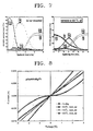
- Fig. 7 is graphs showing the AES (Auger Electron Spectroscopy) depth profile of a nickel-magnesium (Ni-Mg) solid solution used for fabricating a thin film electrode according to a preferred embodiment of the present invention.
- Fig. 7(a) represents the results prior to annealing
- Fig. 7(b) represents the results after annealing at 550°C for 1 minute;
- Fig. 7(a) it was observed that nickel (Ni) and a small amount of magnesium (Mg) remain on the surface of the gallium nitride layer. Although not shown in Fig. 7(a) , the AES data related with magnesium (Mg) reveals that magnesium (Mg) is solubilized in nickel (Ni), rather than is formed into a compound through a reaction with nickel (Ni). Fig. 7(b) apparently shows that the nickel-magnesium solid solution is formed and at the same time an extremely small amount of magnesium is diffused into the surface of gallium nitride and distributed.
- Fig. 8 is a graph showing current-voltage characteristic before and after annealing in air, following depositing a nickel-magnesium (Ni-Mg) solid solution/platinum (Pt) on a p-type gallium nitride layer having a carrier concentration of 5 x 10 17 in accordance with an embodiment of the present invention.
- Ni-Mg nickel-magnesium
- Pt platinum
- a p-type gallium nitride layer having a carrier concentration of 5 x 10 17 in accordance with an embodiment of the present invention.
- Fig. 9 is a graph showing current-voltage characteristics before and after annealing in air, following depositing a nickel-magnesium (Ni-Mg) solid solution/palladium (Pd) on a p-type gallium nitride layer having a carrier concentration of 5 x 10 17 in accordance with an embodiment of the present invention.
- Ni-Mg nickel-magnesium
- Pd palladium
- Fig. 10 is a graph showing current-voltage characteristics before and after annealing in air, following depositing a nickel-magnesium (Ni-Mg) solid solution/ruthenium (Ru) on a p-type gallium nitride layer having a carrier concentration of 5 x 10 17 in accordance with an embodiment of the present invention.
- Ni-Mg nickel-magnesium
- Ru ruthenium
- Fig. 11 is a graph showing current-voltage characteristics before and after annealing in air, following depositing a ruthenium (Ru)/nickel-magnesium (Ni-Mg) solid solution on a p-type gallium nitride layer having a carrier concentration of 5 x 10 17 in accordance with an embodiment of the present invention.
- ruthenium (Ru)/nickel-magnesium (Ni-Mg) solid solution on a p-type gallium nitride layer having a carrier concentration of 5 x 10 17 in accordance with an embodiment of the present invention.
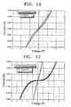
- Fig. 12 is a graph showing current-voltage characteristic before and after annealing in air, following depositing a nickel-zinc (Ni-Zn) solid solution/gold (Au) on a p-type gallium nitride layer having a carrier concentration of 5 x 10 17 in accordance with an embodiment of the present invention.
- Ni-Zn nickel-zinc
- Au gold
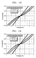
- Fig. 13 is a graph showing current-voltage characteristic before and after annealing in air, following depositing a pure nickel (Ni)/nickel-zinc (Ni-Zn) solid solution/gold (Au) on a p-type gallium nitride layer having a carrier concentration of 5 x 10 17 in accordance with an embodiment of the present invention.
- Fig. 14 is a graph showing current-voltage characteristic before and after annealing in air, following depositing a nickel-zinc (Ni-Zn) solid solution/nickel (Ni)/gold (Au) on a p-type gallium nitride layer having a carrier concentration of 5 x 10 17 in accordance with an embodiment of the present invention.
- Ni-Zn nickel-zinc
- Ni nickel-zinc
- Au gold
- a p-type gallium nitride (GaN) layer was placed in an ultrasonic bath, and then washed at 60°C for 5 minutes using trichloroethylene, acetone, methanol and distilled water, respectively.
- the washed p-type gallium nitride layer was subjected to a hard baking process at 100°C for 10 minutes to completely remove moisture remaining on the p-type gallium nitride layer.
- a Photoresist was spin-coated at 4,000rpm onto the p-type gallium nitride layer, and then subjected to a soft baking process at 88°C for 10 minutes.
- a mask was aligned with the GaN layer and exposed to a UV light at an intensity of 22.8mW for 10 seconds, the resulting structure was dipped in a mixture of a developing agent and distilled water (1:4), and developed for 15 seconds.
- the developed sample was dipped in BOE solution for 5 minutes to remove contaminants remaining on the sample.
- a nickel-magnesium (Ni-Mg) solid solution/gold (Au) was deposited on the developed sample in a thickness of 100 ⁇ using an electron-beam evaporator, and then subjected to a lift-off process using acetone.
- the resulting structure was charged into a rapid thermal annealing (RTA) furnace and annealed under air or nitrogen gas at 350 ⁇ 550°C for 1 minute to fabricate a high-grade thin film electrode for forming an ohmic contact.
- RTA rapid thermal annealing
- a procedure was performed in the same manner as in Example 1 up to the step of depositing a Ni-Mg solid solution. Thereafter, platinum (Pt) was deposited using an electron-beam evaporator to form a capping layer in a thickness of 100 ⁇ , and then subjected to a lift-off process using acetone. The resulting structure was charged into a rapid thermal annealing (RTA) furnace and annealed in air at 450 ⁇ 650°C for 1 minute to fabricate a thin metal film for forming an ohmic contact.
- RTA rapid thermal annealing
- a procedure was performed in the same manner as in Example 1 up to the step of depositing a Ni-Mg solid solution. Thereafter, palladium (Pd) was deposited using an electron-beam evaporator to form a capping layer in a thickness of 100 ⁇ , and then subjected to a lift-off process using acetone. The resulting structure was charged into a rapid thermal annealing (RTA) furnace and annealed in air at 450°C for 1 minute to fabricate a thin metal film for forming an ohmic contact.
- RTA rapid thermal annealing
- a procedure was performed in the same manner as in Example 1 up to the step of depositing an electrode layer on a gallium nitride layer. Thereafter, ruthenium (Ru), a nickel-magnesium (Ni-Mg) solid solution and gold (Au) were sequentially deposited in thicknesses of 50 ⁇ and 50 ⁇ , respectively, using an electron-beam evaporator and then subjected to a lift-off process using acetone. The resulting structure was charged into a rapid thermal annealing (RTA) furnace and annealed in air at 350 ⁇ 650°C for 1 minute to fabricate a thin metal film for forming an ohmic contact.
- RTA rapid thermal annealing
- a procedure was performed in the same manner as in Example 1 up to the step of depositing a Ni-Mg solid solution in a thickness of 50 ⁇ . Thereafter, ruthenium (Ru) was deposited using an electron-beam evaporator to form a capping layer in a thickness of 50 ⁇ , and then subjected to a lift-off process using acetone. The resulting structure was charged into a rapid thermal annealing (RTA) furnace and annealed in air at 450°C for 1 minute to fabricate a thin metal film for forming an ohmic contact.
- RTA rapid thermal annealing
- a procedure was performed in the same manner as in Example 1 up to the step of depositing a Ni-Zn solid solution in a thickness of 50 ⁇ . Thereafter, gold (Au) was deposited using an electron-beam evaporator to form a capping layer in a thickness of 50 ⁇ , and then subjected to a lift-off process using acetone. The resulting structure was charged into a rapid thermal annealing (RTA) furnace and annealed in air at 350 ⁇ 650°C for 1 minute to fabricate a thin metal film for forming an ohmic contact.
- RTA rapid thermal annealing
- a procedure was performed in the same manner as in Example 1 up to the step of depositing a Ni-Zn solid solution in a thickness of 30 ⁇ . Thereafter, nickel (Ni) and gold (Au) were deposited in thicknesses of 20 ⁇ and 50 ⁇ , respectively, using an electron-beam evaporator, and then subjected to a lift-off process using acetone. The resulting structure was charged into a rapid thermal annealing (RTA) furnace and annealed in air at 350 ⁇ 650°C for 1 minute to fabricate a thin metal film for forming an ohmic contact.
- RTA rapid thermal annealing
- a procedure was performed in the same manner as in Example 1 up to the step of depositing an electrode layer on a gallium nitride layer. Thereafter, nickel-(Ni), a nickel-zinc (Ni-Zn) solid solution and gold (Au) were sequentially deposited in thicknesses of 20 ⁇ , 30 ⁇ and 50 ⁇ , respectively, using an electron-beam evaporator and then subjected to a lift-off process using acetone. The resulting structure was charged into a rapid thermal annealing (RTA) furnace and annealed in air at 350 ⁇ 650°C for 1 minute to fabricate a thin metal film for forming an ohmic contact.
- RTA rapid thermal annealing
- the thin film electrode for forming an ohmic contact of the present invention is expected to exhibit excellent electrical and optical properties such as low specific contact resistance, excellent current-voltage characteristics, good surface state and high transparence, in particular improved current injection and spreading capabilities. Accordingly, since the thin film electrode for forming an ohmic contact of the present invention can considerably improve electrical and optical efficiencies of gallium nitride light emitting diodes (LEDs) and laser diodes (LDs), it can be utilized in the development of light emitting diodes and laser diodes with high quality in the near future.
- LEDs gallium nitride light emitting diodes
- LDs laser diodes
Landscapes
- Physics & Mathematics (AREA)
- Condensed Matter Physics & Semiconductors (AREA)
- General Physics & Mathematics (AREA)
- Electromagnetism (AREA)
- Optics & Photonics (AREA)
- Electrodes Of Semiconductors (AREA)
- Semiconductor Lasers (AREA)
- Led Devices (AREA)
Claims (12)
- Electrode à film mince permettant d'établir un contact ohmique dans des diodes électroluminescentes ou des diodes laser, comprenant:une première couche d'électrode (3) stratifiée sur une couche de nitrure de gallium (2) de type p ou une couche AlxInyGazN de type P, etune deuxième couche d'électrode (4) stratifiée sur la première couche d'électrode (3) ;où la première couche d'électrode (3) comprend une solution solide Ni-X ; etla deuxième couche d'électrode (4) comprend au moins un élément sélectionné parmi le groupe consistant en Au, Pt, Pd, Ni, Ru, Rh, Re, C, Cu, Al, Ag and Ir ou au moins un composé sélectionné parmi le groupe consistant en oxydes conducteurs transparents et nitrures conducteurs transparents ; où 0 < x < 1, 0 < y < 1, 0 < z < 1 et x + y + z = 1;où la solution solide (Ni-X) à base de Ni contient du nickel (Ni) comme métal matriciel, et X comprenant au moins un élément sélectionné parmi le groupe consistant en éléments de groupe II, éléments de groupe VI, Sc, Y, Ge, Sn et Sb.
- Electrode à film mince selon la revendication 1, où la deuxième couche d'électrode (4) comprend au moins un élément sélectionné parmi le groupe consistant en Au, Pt, Pd, Ni, Ru, Rh, Re, C, Cu et Ir.
- Electrode à film mince selon la revendication 1 ou 2, comprenant en outre une troisième couche d'électrode (5) stratifiée sur la deuxième couche d'électrode (4) et contenant au moins un composé sélectionné parmi le groupe consistant en oxydes conducteurs transparents et nitrures conducteurs transparents.
- Electrode à film mince selon la revendication 3, comprenant en outre une quatrième couche d'électrode (6) stratifiée sur la troisième couche d'électrode et comprenant au moins un élément sélectionné parmi le groupe consistant en Al, Ag et Rh.
- Electrode à film mince selon la revendication 1, où la deuxième couche d'électrode (4) contient au moins un composé sélectionné parmi le groupe consistant en oxydes conducteurs transparents et nitrures conducteurs transparents.
- Electrode à film mince selon la revendication 1, 2 ou 5, comprenant en outre une troisième électrode (5) stratifiée sur la deuxième couche d'électrode (4) et comprenant au moins un élément sélectionné parmi le groupe consistant en Al, Ag et Rh.
- Electrode à film mince selon la revendication 1, où la deuxième couche d'électrode (4) comprend au moins un élément sélectionné parmi le groupe consistant en Al, Ag et Rh.
- Electrode à film mince selon l'une des revendications précédentes, où X est un élément de groupe II contenant un élément sélectionné parmi le groupe consistant en Mg, Be, Ca et Zn.
- Electrode à film mince selon l'une quelconque des revendications 1 à 7, où X est un élément de groupe VI contenant un élément sélectionné parmi le groupe consistant en S, Se et Te.
- Electrode à film mince selon l'une quelconque des revendications 1 à 7, où l'on ajoute l'élément X constituant la solution solide à base de Ni (Ni-X) dans une quantité de 1 à 49 pour-cent atomiques (%).
- Electrode à film mince selon l'une quelconque des revendications 1 à 7, où les couches d'électrode (3,4) formées à partir de la solution solide à base de Ni ont une épaisseur de 1 à 1000 Angstroms, et la première, la deuxième, la troisième et la quatrième couches d'électrode (3,4,5,6) ont une épaisseur globale de 1-10.000 Angstroms.
- Procédé de fabrication d'une électrode à film mince sur une couche à base de nitrure de gallium de type p, comprenant les phases suivantes:lavage des couches d'oxygène et à base de carbone sur un semi-conducteur de nitrure de gallium pour en retirer les impuretés ;déposition d'une solution solide à base de nickel sous vide poussé de 2,66 x 10⁻⁴ Pa à 6, 66 x 10-6 Pa (2 x 10⁻⁶ à 5 x 10⁻⁸ torr) par évaporation par faisceau d'électrons, évaporation par rayon d'électrons, procédé de pulvérisation cathodique, déposition de laser plasma ou procédé électrochimique ; etrecuit de la solution solide à base de nickel déposée Ni-X sous air, oxygène ou atmosphère d'azote à 250∼800°C pendant 30 secondes à 1 heure ;et formation d'une deuxième couche d'électrode comprenant au moins un élément sélectionné parmi le groupe consistant en Au, Pt, Pd, Ni, Ru, Rh, Re, C, Cu, Al, Ag et Ir ou au moins un composé sélectionné parmi le groupe consistant en oxydes conducteurs transparents et nitrures conducteurs transparents;où la solution solide à base de nickel contient du nickel (Ni) comme métal matriciel, et X contenant au moins un élément sélectionné parmi le groupe consistant en éléments de groupe II, éléments de groupe VI, Sc, Y, Ge, Sn et Sb,où la couche à base de nitrure de gallium de type p est le nitrure de gallium ou présente une composition d'AlxInyGazN (où 0 < x < 1, 0 < y < 1, 0 < z < 1 et x + y + z = 1).
Applications Claiming Priority (2)
| Application Number | Priority Date | Filing Date | Title |
|---|---|---|---|
| KR2003029073 | 2003-05-07 | ||
| KR1020030029073A KR100612832B1 (ko) | 2003-05-07 | 2003-05-07 | 고성능의 질화갈륨계 광소자 구현을 위한 니켈계 고용체를 이용한 오믹 접촉 형성을 위한 금속박막 및 그 제조방법 |
Publications (2)
| Publication Number | Publication Date |
|---|---|
| EP1475845A1 EP1475845A1 (fr) | 2004-11-10 |
| EP1475845B1 true EP1475845B1 (fr) | 2015-06-10 |
Family
ID=36385331
Family Applications (1)
| Application Number | Title | Priority Date | Filing Date |
|---|---|---|---|
| EP04251791.2A Expired - Lifetime EP1475845B1 (fr) | 2003-05-07 | 2004-03-26 | Contacts ohmiques de base Ni d' une solution solide pour GaN de p-type en LEDs |
Country Status (5)
| Country | Link |
|---|---|
| US (2) | US6989598B2 (fr) |
| EP (1) | EP1475845B1 (fr) |
| JP (2) | JP4803968B2 (fr) |
| KR (1) | KR100612832B1 (fr) |
| CN (1) | CN100517774C (fr) |
Families Citing this family (33)
| Publication number | Priority date | Publication date | Assignee | Title |
|---|---|---|---|---|
| KR100624411B1 (ko) * | 2003-08-25 | 2006-09-18 | 삼성전자주식회사 | 질화물계 발광소자 및 그 제조방법 |
| KR100647278B1 (ko) * | 2003-10-27 | 2006-11-17 | 삼성전자주식회사 | III - V 족 GaN 계 화합물 반도체 및 이에적용되는 p-형 전극 |
| KR100590532B1 (ko) * | 2003-12-22 | 2006-06-15 | 삼성전자주식회사 | 플립칩형 질화물계 발광소자 및 그 제조방법 |
| CN100401541C (zh) * | 2005-01-14 | 2008-07-09 | 财团法人工业技术研究院 | 一种量子点/量子阱发光二极管 |
| US7932111B2 (en) * | 2005-02-23 | 2011-04-26 | Cree, Inc. | Substrate removal process for high light extraction LEDs |
| KR100878433B1 (ko) * | 2005-05-18 | 2009-01-13 | 삼성전기주식회사 | 발광소자의 오믹컨택층 제조방법 및 이를 이용한발광소자의 제조방법 |
| JP5138873B2 (ja) * | 2005-05-19 | 2013-02-06 | 日亜化学工業株式会社 | 窒化物半導体素子 |
| KR20070035660A (ko) * | 2005-09-28 | 2007-04-02 | 엘지이노텍 주식회사 | 질화물 반도체 발광소자 제조방법 |
| EP2005488B1 (fr) | 2005-12-16 | 2013-07-31 | Samsung Display Co., Ltd. | Dispositif optique et procédé de fabrication |
| JP5244614B2 (ja) * | 2005-12-27 | 2013-07-24 | 三星ディスプレイ株式會社 | Iii族窒化物系発光素子 |
| CN1851941A (zh) * | 2006-04-30 | 2006-10-25 | 普光科技(广州)有限公司 | 一种制造氮化镓发光二极管芯片的工艺方法 |
| JP4884866B2 (ja) * | 2006-07-25 | 2012-02-29 | 三菱電機株式会社 | 窒化物半導体装置の製造方法 |
| KR100845037B1 (ko) * | 2006-08-02 | 2008-07-09 | 포항공과대학교 산학협력단 | 오믹 전극 및 그 형성 방법, 이를 구비하는 반도체 발광소자 |
| JP5522648B2 (ja) * | 2008-04-01 | 2014-06-18 | 独立行政法人産業技術総合研究所 | ダイヤモンド表面と金属片との接合保護構造 |
| US8816356B2 (en) | 2008-09-30 | 2014-08-26 | Youngstown State University | Silicon carbide barrier diode |
| EP2273573A4 (fr) * | 2009-03-11 | 2012-11-14 | Panasonic Corp | Elément à semi-conducteur nitrure et procédé pour sa fabrication |
| WO2010113238A1 (fr) * | 2009-04-03 | 2010-10-07 | パナソニック株式会社 | Élément à semi-conducteurs de nitrure et son procédé de fabrication |
| WO2010113237A1 (fr) * | 2009-04-03 | 2010-10-07 | パナソニック株式会社 | Élément à semi-conducteurs de nitrure et son procédé de fabrication |
| CN102482073B (zh) * | 2009-08-24 | 2016-04-27 | 卡文迪什动力有限公司 | 用于光调制的浮动摇臂mems器件的制造 |
| EP2541624A4 (fr) | 2010-04-01 | 2013-05-15 | Panasonic Corp | Élément semi-conducteur de nitrure et procédé de fabrication de celui-ci |
| CN102214762A (zh) * | 2010-04-06 | 2011-10-12 | 尚安品有限公司 | 发光二极管芯片及其封装结构 |
| JP2012164718A (ja) * | 2011-02-03 | 2012-08-30 | Advanced Power Device Research Association | 半導体デバイスおよび半導体デバイス製造方法 |
| US9818912B2 (en) * | 2011-12-12 | 2017-11-14 | Sensor Electronic Technology, Inc. | Ultraviolet reflective contact |
| CN102569581B (zh) * | 2012-02-28 | 2015-07-01 | 江苏新广联科技股份有限公司 | 具有重叠电极的led芯片结构 |
| JP5607676B2 (ja) * | 2012-04-17 | 2014-10-15 | 国立大学法人電気通信大学 | 整流素子 |
| KR20130127209A (ko) * | 2012-05-14 | 2013-11-22 | 삼성전자주식회사 | 질화갈륨계 반도체 발광소자의 제조방법 |
| JP6340016B2 (ja) * | 2013-01-24 | 2018-06-06 | コーニンクレッカ フィリップス エヌ ヴェKoninklijke Philips N.V. | 半導体発光デバイスにおけるpコンタクト抵抗の制御 |
| JP6260159B2 (ja) * | 2013-09-17 | 2018-01-17 | 沖電気工業株式会社 | 窒化物半導体発光ダイオード、及びその製造方法 |
| EP2881982B1 (fr) * | 2013-12-05 | 2019-09-04 | IMEC vzw | Procédé de fabrication de couches de contact compatibles CMOS dans des dispositifs à semi-conducteurs |
| JP7308831B2 (ja) * | 2017-12-14 | 2023-07-14 | ルミレッズ リミテッド ライアビリティ カンパニー | Ledダイの汚染を防止する方法 |
| US12142642B2 (en) * | 2018-06-20 | 2024-11-12 | Lawrence Livermore National Security, Llc | Field assisted interfacial diffusion doping through heterostructure design |
| KR102544296B1 (ko) * | 2018-09-13 | 2023-06-16 | 쑤저우 레킨 세미컨덕터 컴퍼니 리미티드 | 표면발광레이저 소자 및 이를 구비한 표면발광레이저 장치 |
| WO2020121794A1 (fr) | 2018-12-11 | 2020-06-18 | パナソニックセミコンダクターソリューションズ株式会社 | Élément électroluminescent à semi-conducteur au nitrure, son procédé de fabrication, et procédé de fabrication d'un cristal semi-conducteur au nitrure |
Family Cites Families (30)
| Publication number | Priority date | Publication date | Assignee | Title |
|---|---|---|---|---|
| JP3494478B2 (ja) * | 1994-08-22 | 2004-02-09 | 日亜化学工業株式会社 | 窒化ガリウム系化合物半導体素子 |
| JPH0936423A (ja) * | 1995-07-24 | 1997-02-07 | Toyoda Gosei Co Ltd | 3族窒化物半導体発光素子 |
| JP3760478B2 (ja) * | 1995-05-18 | 2006-03-29 | 昭和電工株式会社 | Iii−v族化合物半導体素子の製造方法 |
| JP3620926B2 (ja) * | 1995-06-16 | 2005-02-16 | 豊田合成株式会社 | p伝導形3族窒化物半導体の電極及び電極形成方法及び素子 |
| JP3009095B2 (ja) * | 1995-10-27 | 2000-02-14 | 日亜化学工業株式会社 | 窒化物半導体発光素子 |
| JP3269070B2 (ja) * | 1995-10-30 | 2002-03-25 | 日亜化学工業株式会社 | 窒化物半導体発光素子 |
| JPH10209072A (ja) * | 1997-01-17 | 1998-08-07 | Matsushita Electric Ind Co Ltd | 窒化物化合物半導体の電極形成方法 |
| JPH10303460A (ja) * | 1997-02-27 | 1998-11-13 | Toshiba Corp | 半導体素子およびその製造方法 |
| JPH10247747A (ja) * | 1997-03-05 | 1998-09-14 | Toshiba Corp | 半導体発光素子およびその製造方法 |
| JP3807020B2 (ja) * | 1997-05-08 | 2006-08-09 | 昭和電工株式会社 | 発光半導体素子用透光性電極およびその作製方法 |
| JPH10308533A (ja) * | 1997-05-09 | 1998-11-17 | Toshiba Corp | 窒化ガリウム系化合物半導体発光素子およびその製造方法ならびに発光装置 |
| JP3299145B2 (ja) * | 1997-07-15 | 2002-07-08 | 日本電気株式会社 | 窒化ガリウム系半導体のp型電極およびその形成方法 |
| JP3130292B2 (ja) * | 1997-10-14 | 2001-01-31 | 松下電子工業株式会社 | 半導体発光装置及びその製造方法 |
| KR19990052640A (ko) * | 1997-12-23 | 1999-07-15 | 김효근 | 오믹접촉 형성을 이용한 다이오드용 금속박막및 그의 제조방법 |
| US6078064A (en) | 1998-05-04 | 2000-06-20 | Epistar Co. | Indium gallium nitride light emitting diode |
| JP3736181B2 (ja) * | 1998-05-13 | 2006-01-18 | 豊田合成株式会社 | Iii族窒化物系化合物半導体発光素子 |
| KR100293467B1 (ko) | 1998-06-12 | 2001-07-12 | 구자홍 | 청색발광소자및그제조방법 |
| JP3413102B2 (ja) * | 1998-06-30 | 2003-06-03 | 古河電気工業株式会社 | p型半導体層用電極 |
| TW386286B (en) | 1998-10-26 | 2000-04-01 | Ind Tech Res Inst | An ohmic contact of semiconductor and the manufacturing method |
| JP4292619B2 (ja) * | 1999-03-24 | 2009-07-08 | パナソニック株式会社 | 半導体装置の製造方法 |
| JP3555512B2 (ja) | 1999-07-22 | 2004-08-18 | 日立電線株式会社 | p型窒化ガリウム系化合物半導体の製造方法 |
| JP3068914U (ja) * | 1999-11-11 | 2000-05-26 | 洲磊科技股▲ふん▼有限公司 | フリップ―チップ発光デバイス |
| TW465123B (en) * | 2000-02-02 | 2001-11-21 | Ind Tech Res Inst | High power white light LED |
| JP2001217456A (ja) * | 2000-02-03 | 2001-08-10 | Sharp Corp | 窒化ガリウム系化合物半導体発光素子 |
| US6693352B1 (en) * | 2000-06-05 | 2004-02-17 | Emitronix Inc. | Contact structure for group III-V semiconductor devices and method of producing the same |
| JP4024994B2 (ja) * | 2000-06-30 | 2007-12-19 | 株式会社東芝 | 半導体発光素子 |
| JP2002164575A (ja) * | 2000-11-27 | 2002-06-07 | Nichia Chem Ind Ltd | 窒化物半導体発光素子 |
| JP4101468B2 (ja) | 2001-04-09 | 2008-06-18 | 豊田合成株式会社 | 発光装置の製造方法 |
| US6649942B2 (en) * | 2001-05-23 | 2003-11-18 | Sanyo Electric Co., Ltd. | Nitride-based semiconductor light-emitting device |
| JP2003258304A (ja) * | 2002-02-28 | 2003-09-12 | Hitachi Cable Ltd | 半導体発光素子及びその製造方法 |
-
2003
- 2003-05-07 KR KR1020030029073A patent/KR100612832B1/ko not_active Expired - Fee Related
-
2004
- 2004-03-17 US US10/801,823 patent/US6989598B2/en not_active Expired - Lifetime
- 2004-03-26 CN CNB2004100312461A patent/CN100517774C/zh not_active Expired - Lifetime
- 2004-03-26 EP EP04251791.2A patent/EP1475845B1/fr not_active Expired - Lifetime
- 2004-03-31 JP JP2004104946A patent/JP4803968B2/ja not_active Expired - Fee Related
-
2005
- 2005-11-03 US US11/265,098 patent/US7550374B2/en not_active Expired - Lifetime
-
2011
- 2011-06-28 JP JP2011143316A patent/JP5164291B2/ja not_active Expired - Fee Related
Also Published As
| Publication number | Publication date |
|---|---|
| EP1475845A1 (fr) | 2004-11-10 |
| US6989598B2 (en) | 2006-01-24 |
| JP5164291B2 (ja) | 2013-03-21 |
| US20060102920A1 (en) | 2006-05-18 |
| KR20040096207A (ko) | 2004-11-16 |
| US7550374B2 (en) | 2009-06-23 |
| JP4803968B2 (ja) | 2011-10-26 |
| US20040222524A1 (en) | 2004-11-11 |
| JP2011199319A (ja) | 2011-10-06 |
| CN100517774C (zh) | 2009-07-22 |
| KR100612832B1 (ko) | 2006-08-18 |
| JP2004336021A (ja) | 2004-11-25 |
| CN1622348A (zh) | 2005-06-01 |
Similar Documents
| Publication | Publication Date | Title |
|---|---|---|
| EP1475845B1 (fr) | Contacts ohmiques de base Ni d' une solution solide pour GaN de p-type en LEDs | |
| EP2262013B1 (fr) | Procédé de fabrication d'une diode électroluminescente basée sur nitrure de gallium | |
| CN100361324C (zh) | 氮化物基发光器件及其制造方法 | |
| US20050199888A1 (en) | Top-emitting nitride-based light-emitting device and method of manufacturing the same | |
| GB2351605A (en) | Method of forming light transmissive contact of a light source | |
| US20070254391A1 (en) | Light emitting device and method of manufacturing the same | |
| KR100707167B1 (ko) | 고성능의 질화갈륨계 광소자 구현을 위한 p형 열전산화물을 형성하는 2원계 및 3원계 합금 또는 고용체박막을 이용한 오믹접촉 형성을 위한 박막전극 및 그제조방법 | |
| KR20000040564A (ko) | 질화물 청색 발광소자의 도전성 투명 산화막 전극 제작 방법 | |
| KR100561841B1 (ko) | 고품위 발광다이오드 및 레이저 다이오드의 구현을 위한질화 갈륨을 포함하는 p형 반도체의 오믹접촉형성을 위한투명박막전극 | |
| KR20060007948A (ko) | 탑에미트형 질화물계 발광소자 및 그 제조방법 | |
| KR100515652B1 (ko) | p형 질화갈륨(GaN) 반도체의 오믹접촉형성을 위한투명전극박막 | |
| US8735195B2 (en) | Method of manufacturing a zinc oxide (ZnO) based semiconductor device including performing a heat treatment of a contact metal layer on a p-type ZnO semiconductor layer in a reductive gas atmosphere | |
| KR100611642B1 (ko) | 탑에미트형 질화물계 발광소자 및 그 제조방법 | |
| KR100601971B1 (ko) | 탑에미트형 질화물계 발광소자 및 그 제조방법 | |
| KR100574105B1 (ko) | 탑에미트형 질화물계 발광소자 및 그 제조방법 | |
| KR20050079209A (ko) | 전극층, 이를 구비하는 발광소자 및 전극층 제조방법 | |
| KR20060007945A (ko) | 탑에미트형 질화물계 발광소자 및 그 제조방법 |
Legal Events
| Date | Code | Title | Description |
|---|---|---|---|
| PUAI | Public reference made under article 153(3) epc to a published international application that has entered the european phase |
Free format text: ORIGINAL CODE: 0009012 |
|
| AK | Designated contracting states |
Kind code of ref document: A1 Designated state(s): AT BE BG CH CY CZ DE DK EE ES FI FR GB GR HU IE IT LI LU MC NL PL PT RO SE SI SK TR |
|
| AX | Request for extension of the european patent |
Extension state: AL LT LV MK |
|
| 17P | Request for examination filed |
Effective date: 20050202 |
|
| AKX | Designation fees paid |
Designated state(s): DE FR GB |
|
| 17Q | First examination report despatched |
Effective date: 20100413 |
|
| RAP1 | Party data changed (applicant data changed or rights of an application transferred) |
Owner name: KWANGJU INSTITUTE OF SCIENCE AND TECHNOLOGY Owner name: SAMSUNG LED CO., LTD. |
|
| RAP1 | Party data changed (applicant data changed or rights of an application transferred) |
Owner name: SAMSUNG ELECTRONICS CO., LTD. Owner name: KWANGJU INSTITUTE OF SCIENCE AND TECHNOLOGY |
|
| RIC1 | Information provided on ipc code assigned before grant |
Ipc: H01L 33/40 20100101ALI20140901BHEP Ipc: H01L 33/00 20100101AFI20140901BHEP |
|
| GRAP | Despatch of communication of intention to grant a patent |
Free format text: ORIGINAL CODE: EPIDOSNIGR1 |
|
| INTG | Intention to grant announced |
Effective date: 20141222 |
|
| GRAS | Grant fee paid |
Free format text: ORIGINAL CODE: EPIDOSNIGR3 |
|
| GRAA | (expected) grant |
Free format text: ORIGINAL CODE: 0009210 |
|
| AK | Designated contracting states |
Kind code of ref document: B1 Designated state(s): DE FR GB |
|
| REG | Reference to a national code |
Ref country code: GB Ref legal event code: FG4D |
|
| REG | Reference to a national code |
Ref country code: DE Ref legal event code: R096 Ref document number: 602004047331 Country of ref document: DE |
|
| REG | Reference to a national code |
Ref country code: DE Ref legal event code: R097 Ref document number: 602004047331 Country of ref document: DE |
|
| PLBE | No opposition filed within time limit |
Free format text: ORIGINAL CODE: 0009261 |
|
| STAA | Information on the status of an ep patent application or granted ep patent |
Free format text: STATUS: NO OPPOSITION FILED WITHIN TIME LIMIT |
|
| 26N | No opposition filed |
Effective date: 20160311 |
|
| GBPC | Gb: european patent ceased through non-payment of renewal fee |
Effective date: 20160326 |
|
| REG | Reference to a national code |
Ref country code: FR Ref legal event code: ST Effective date: 20161130 |
|
| PG25 | Lapsed in a contracting state [announced via postgrant information from national office to epo] |
Ref country code: GB Free format text: LAPSE BECAUSE OF NON-PAYMENT OF DUE FEES Effective date: 20160326 Ref country code: FR Free format text: LAPSE BECAUSE OF NON-PAYMENT OF DUE FEES Effective date: 20160331 |
|
| PGFP | Annual fee paid to national office [announced via postgrant information from national office to epo] |
Ref country code: DE Payment date: 20230131 Year of fee payment: 20 |
|
| P01 | Opt-out of the competence of the unified patent court (upc) registered |
Effective date: 20230524 |
|
| REG | Reference to a national code |
Ref country code: DE Ref legal event code: R071 Ref document number: 602004047331 Country of ref document: DE |