EP1480068B1 - Dispositif de modulation de la lumière du type réseau, sa méthode de commande, et dispositif d'affichage à panneau plat - Google Patents
Dispositif de modulation de la lumière du type réseau, sa méthode de commande, et dispositif d'affichage à panneau plat Download PDFInfo
- Publication number
- EP1480068B1 EP1480068B1 EP04013886A EP04013886A EP1480068B1 EP 1480068 B1 EP1480068 B1 EP 1480068B1 EP 04013886 A EP04013886 A EP 04013886A EP 04013886 A EP04013886 A EP 04013886A EP 1480068 B1 EP1480068 B1 EP 1480068B1
- Authority
- EP
- European Patent Office
- Prior art keywords
- needle
- light modulation
- modulation element
- light
- array
- Prior art date
- Legal status (The legal status is an assumption and is not a legal conclusion. Google has not performed a legal analysis and makes no representation as to the accuracy of the status listed.)
- Expired - Lifetime
Links
- 238000000034 method Methods 0.000 title claims description 21
- 230000005540 biological transmission Effects 0.000 claims description 55
- 239000000758 substrate Substances 0.000 claims description 49
- 238000006073 displacement reaction Methods 0.000 claims description 36
- 230000004044 response Effects 0.000 claims description 24
- 239000000463 material Substances 0.000 claims description 22
- 230000000694 effects Effects 0.000 claims description 12
- 230000003287 optical effect Effects 0.000 claims description 5
- 230000005684 electric field Effects 0.000 claims description 3
- 230000007423 decrease Effects 0.000 claims description 2
- 239000011159 matrix material Substances 0.000 description 34
- 230000007935 neutral effect Effects 0.000 description 27
- 239000004973 liquid crystal related substance Substances 0.000 description 20
- 239000004020 conductor Substances 0.000 description 12
- 238000004519 manufacturing process Methods 0.000 description 5
- 230000008859 change Effects 0.000 description 4
- 239000012212 insulator Substances 0.000 description 3
- 230000003247 decreasing effect Effects 0.000 description 2
- 230000003111 delayed effect Effects 0.000 description 2
- 230000004907 flux Effects 0.000 description 2
- 239000004642 Polyimide Substances 0.000 description 1
- 239000003990 capacitor Substances 0.000 description 1
- 239000003086 colorant Substances 0.000 description 1
- 230000001419 dependent effect Effects 0.000 description 1
- 238000009792 diffusion process Methods 0.000 description 1
- 239000013013 elastic material Substances 0.000 description 1
- 238000005530 etching Methods 0.000 description 1
- 230000006870 function Effects 0.000 description 1
- 239000011521 glass Substances 0.000 description 1
- 238000009413 insulation Methods 0.000 description 1
- 230000003446 memory effect Effects 0.000 description 1
- 238000000206 photolithography Methods 0.000 description 1
- 229920001721 polyimide Polymers 0.000 description 1
- 229920000642 polymer Polymers 0.000 description 1
- 238000002360 preparation method Methods 0.000 description 1
- 230000002265 prevention Effects 0.000 description 1
- 230000002035 prolonged effect Effects 0.000 description 1
- 230000000717 retained effect Effects 0.000 description 1
- 230000000630 rising effect Effects 0.000 description 1
- 238000007789 sealing Methods 0.000 description 1
- 239000004065 semiconductor Substances 0.000 description 1
- 125000006850 spacer group Chemical group 0.000 description 1
- 230000007704 transition Effects 0.000 description 1
Images


Classifications
-
- G—PHYSICS
- G02—OPTICS
- G02B—OPTICAL ELEMENTS, SYSTEMS OR APPARATUS
- G02B26/00—Optical devices or arrangements for the control of light using movable or deformable optical elements
- G02B26/02—Optical devices or arrangements for the control of light using movable or deformable optical elements for controlling the intensity of light
Definitions
- This invention relates to an array-type light modulation element according to the preamble of claim 1. It also relates to a flat panel display, which makes use of such array type light modulation element.
- a light modulation element is available for controlling the amplitude (strength), phase, travel direction, etc., of incident light for processing and displaying an image, pattern data, etc.
- One of the light modulation elements is a liquid crystal light modulation element using the electro-optic effect of liquid crystal.
- the liquid crystal light modulation element preferably is used with a liquid crystal display of a thin flat-panel display unit.
- the liquid crystal display has a structure wherein oriented liquid crystal is entered and sealed between substrates forming a pair of conductive transparent films and sandwiched between orthogonal deflecting plates.
- the liquid crystal display produces display by applying a voltage to the conductive transparent film for orienting the liquid crystal molecules in the long axis direction perpendicular to the substrate and changing the transmission factor of light from a backlight.
- liquid crystal display By the way, in the liquid crystal display, light from the backlight is allowed to pass through multiple layers of the deflecting plates, transparent electrodes, and color filter, thus the light use efficiency lowers.
- the high-grade liquid crystal display requires TFTs and liquid crystal must be sealed between two substrates and be oriented, thus it is difficult to provide a large screen. This is a disadvantage of the liquid crystal display. Further, since light is allowed to pass through between the oriented liquid crystal molecules, the viewing angle becomes narrow. This is another disadvantage of the liquid crystal display.
- This light modulation element comprises an alternating pattern of a first shield section having a plurality of drive electrodes insulated from each other arranged in a predetermined spacing in a predetermined direction and a second shield section movable with positive and negative charges electrostatically induced, the first and second shield sections being placed on a transparent substrate.
- the voltage applied to the drive electrode is changed, whereby the relative position between the first and second shield sections is changed by an electrostatic stress between the first and second shield sections, thereby changing the transmission factor of light passing through therebetween for executing light modulation.
- the electrostatically driven light modulation element light from the light source is allowed to pass through only the transparent substrate, so that the light use efficiency can be raised and the light modulation elements can be easily put into an array by photolithography and etching and liquid crystal need not be poured or oriented, thus the manufacturing costs can be reduced and a large area can be easily provided.
- the drive method becomes so-called simple matrix drive for connecting scan signal electrodes and image signal electrodes to the first shield section and the second shield section, scanning the scan signal electrodes in sequence, and applying signal voltages corresponding to the scanned scan signal electrodes to the image signal electrodes.
- the condition of the voltages applied to the scan signal electrodes and the image signal electrodes depends on the hysteresis characteristic and is restricted. To enhance the image quality of contrast, etc., it becomes necessary to optimize the element structure and fit the hysteresis characteristic to the drive condition.
- some liquid crystal displays adopt active matrix drive of adding active elements (TFT, etc.,) to intersection parts of an XY matrix and applying voltage to liquid crystal through the active elements.
- TFT active elements
- scan voltage is applied to scan signal electrodes in sequence and the TFTs connected thereto are turned on in unison.
- a signal is applied from image signal electrodes and charges are accumulated in capacitance of each pixel through the TFTs.
- the TFTs are turned off and the charges accumulated in the pixel capacitance are retained (memorized) intact.
- applied voltage can be set as desired in a wide range and comparatively fast response speed and high contrast can be provided, so that high picture quality can also be provided particularly in a moving picture.
- US-5,062,689 discloses an array-type light modulation element in which a first drive means generates a first electromechanical force for displacing the needle and thereby opening a light modulation area.
- a further drive means is provided for generating a second electromechanical force for displacing the needle into a direction opposite to said first direction so that if the second electromechanical force is applied to the needle, the light modulation area is closed.
- the first and the second electromechanical force thereby, act within the same plane but into opposite directions.
- WO 86/01626 discloses an array-type light modulation element including a plurality of light modulation areas, each area having electrostatically movable flaps, which open or close the light modulation area by applying electrostatic forces to said flaps via a plurality of electrodes which are arranged for X-Y addressing (matrix addressing).
- WO 98/57318 discloses an electrostatic video display having a matrix configuration including row and column capacitors for actuating pixels of the array individually by combining electrostatic forces generated by putting signals onto X-electrodes and Y-electrodes.
- XP 00450049 discloses an array-type light modulation element including a matrix structure of micromirrors which are electromechanically actuated. If actuated, each micromirror is rotated by a certain angle, thereby acting like a flap.
- WO 98/19201 discloses an array-type light modulation element including an array of optical waveguides and mechanical light switches, such light modulation element making use of total reflection and deflection of a light beam injected into a transparent plate. If a light switch is brought into contact with the plate, the light beam is deflected out of the plate by the light switch. If the light switch does not contact the plate, the light beam continues to travel within the transparent plate.
- the needle In the light modulation element, the needle is moved substantially in the horizontal direction by the first electromechanical force, whereby light modulation can be executed and the needle is sucked or attracted substantially in the vertical direction for holding the displacement state of the needle or the electromechanical force is canceled and the displacement state can be canceled.
- the direction of the first electromechanical force is substantially vertical and the direction of the second electromechanical force is substantially horizontal.
- the needle In the light modulation element, the needle is moved substantially in the vertical direction by the first electromechanical force, whereby light modulation can be executed and the needle is sucked or attracted substantially in the horizontal direction for holding the displacement state of the needle or the electromechanical force is canceled and the displacement state can be canceled.
- an array-type light modulation element comprising a plurality of parallel scan signal electrodes, a plurality of image signal electrodes orthogonal to the scan signal electrodes, the elements being placed at intersection points of the scan signal electrodes and the image signal electrodes, characterized in that the displacement state of each needle is held or canceled by a signal of the scan signal electrode and the displacement state of each needle is changed by a signal of the image signal electrode.
- the needle is displaced by the signal of the image signal electrode for changing the light transmission factor and the displacement state of the needle can be held or canceled by the signal of the scan signal electrode disposed in the direction orthogonal to the image signal electrode; the light modulation state can be provided with a memory property according to a simple configuration without providing the electrode connected separately to each needle.
- active matrix drive is enabled.
- an array-type light modulation element comprising a plurality of parallel scan signal electrodes, a plurality of latch signal electrodes being placed side by side with the scan signal electrodes, a plurality of image signal electrodes orthogonal to the scan signal electrodes, the latch signal electrodes and light modulation elements, the elements being placed at intersection points of the scan signal electrodes and the latch signal electrodes and the image signal electrodes, characterized in that the displacement state of each needle is held or canceled by signals of the scan signal electrode and the latch signal electrode and the displacement state of each needle is changed by a signal of the image signal electrode.
- the displacement state of each needle is held or canceled by the signals of the scan signal electrode and the latch signal electrode and the displacement state of each needle can be changed by the signal of the image signal electrode; simply the latch signal electrodes are provided, whereby the light modulation state can be provided with a memory property without changing light modulation control.
- the light modulation element is in a shield state when the needle does not operate and wherein a light transmission factor increases as the needle is displaced from the shield state by an electrostatic force.
- the neutral state in which voltage of rightly the same potential is applied to the image signal electrode and the scan signal electrode is adopted as the shield state of the light modulation element, whereby the light modulation element can execute light modulation from the initial shield state to the light passing-through state.
- the light modulation element is in a light passing-through state when the needle does not operate and wherein a light transmission factor decreases as the needle is displaced by an electrostatic force.
- the neutral state in which voltage of rightly the same potential is applied to the image signal electrode and the scan signal electrode is adopted as the light passing-through state of the light modulation element, whereby the light modulation element can execute light modulation from the initial light passing-through state to the shield state.
- a flat-panel display unit comprising an array-type light modulation element, a surface light source being placed facing the array-type light modulation element, and fluorescent material being placed on an opposite side to the surface light source with the array-type light modulation element between, characterized in that light passing through the array-type light modulation element causes the fluorescent material to emit light for producing display.
- the needle is moved by the electrostatic suction force for changing the light transmission factor of the light modulation element and light emitted from the surface light source via the light modulation element is applied to the fluorescent material, thereby exciting the fluorescent material for emitting light, enabling image display based on image information.
- the light from the light source can be applied directly to the fluorescent material for improving the light use efficiency, and the viewing angle can be widened because of the scattering property of the fluorescent material.
- the needle is operated electromechanically, the drive voltage can be lowered and the light modulation state can be held, thus active matrix drive is enabled and high image quality can also be provided in a moving picture. Further, multiple tone drive is also enabled.
- the light emitted from the light source is ultraviolet light.
- the display unit with ultraviolet light as a light source can be provided.
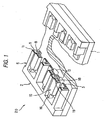
- FIG. 1 is a perspective view of a light modulation element with parts partially broken away according to a first embodiment of the invention
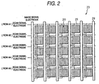
- FIG. 2 is a plan view of an array-type light modulation element comprising the light modulation elements in FIG. 1 arranged like a two-dimensional matrix.
- a grid body 2 is placed on a transparent substrate 1 transparent for light having an insulation property to be modulated.
- the grid body 2 is formed with a plurality of grid walls 5 spaced from each other at given intervals, and a belt-like electric conductor (first fixed electrode) 8 is formed inside each grid wall 5. Further, the electric conductor 8 is covered on the surface with an insulator 9 and is insulated from an adjacent member.
- the grid wall 5 is formed on the upper end face with a shield film 11 for preventing light introduced from below the transparent substrate 1 from being emitted from the upper end face of the grid wall 5.
- the grid walls 5 can be used as a black matrix for improving the contrast ratio.
- the grid walls 5 each being formed with a shield-property conductive film 3 (second fixed electrode) adjoining the grid wall 5 on the transparent electrode 1 on both left and right sides of the grid wall 5 and those formed with nothing on both sides are place alternately.
- the shield-property conductive film 3 is a film body having a shield property and electric conductivity.
- the area in which the shield-property conductive film 3 is not formed between the adjacent grid walls 5 becomes a light modulation area 13 and the light introduced from below the transparent substrate 1 passes through the light modulation area 13 and is emitted to the top side of the transparent substrate 1.
- a needle 15 is disposed above the light modulation area 13. It comprises a narrow part 16 having a cross-sectional area lessened at both ends in the length direction of the needle, and the narrow parts 16 are connected to the grid body 2. Thus, the narrow parts 16 become weak parts and deformed, whereby the needle 15 can be moved in parallel and vertical directions to the transparent substrate 1.
- the needle 15 is formed with a belt-like electric conductor (charged body) 18 and a shield film 19.
- the electric conductor 18 and the shield film 19 may be formed of a shield-property conductive film in one piece.
- the needle 15 In a neutral state (when the electric conductors are at the same potential), the needle 15 is placed above the light modulation area 13 for preventing light passing through the light modulation area 13 from being emitted to the top side of the light modulation element 20.
- the described light modulation elements 20 can be used for an array-type light modulation element 23.
- the array-type light modulation element 23 comprises a plurality of scan signal electrodes 25 arranged in parallel and a plurality of image signal electrodes 29 arranged in parallel orthogonal to the scan signal electrodes 25 with the light modulation elements 20 being placed at the intersection parts of the scan signal electrodes 25 and the image signal electrodes 29.
- a common electrode exists, but is not shown in FIG. 2.
- FIGS. 3A and 3B are plan views to show one pixel area of the light modulation element; FIG. 3A shows the one pixel area in a neutral state (shield state) and FIG. 3B shows the one pixel area at the write scan time (light passing-through state).
- the shield-property conductive films 3 on the transparent substrate are connected to the scan signal electrode 25, the grid walls (fixed electrodes) 5a placed away from the needles 15 in the neutral state are connected to the image signal electrode 29, and the grid walls (fixed electrodes) 5b close to the needles 15 in the neutral state and the needles 15 are connected to the common electrode 27.
- the electrodes are at the same potential. If all potentials are set to 0 [V] as an example, the light modulation element enters the shield state.
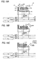
- FIGS. 4A to 4C are sectional views of the main part of the light modulation element 20 shown in FIG. 4A.
- the state shown in FIG. 4A is the initial state (neutral state), in which light from the transparent substrate 1 cannot pass through (shield state) and the voltages of all electrodes are 0 [V].
- the state shown in FIG. 4B is the state at the write scan time and voltage Va [V] responsive to image information is applied to the image signal electrode 29 so as to enter a desired light passing-through state, whereby an electrostatic force (first electromechanical force) occurs at the needles 15 and the needles 15 are sucked and moved in the horizontal direction.
- voltage of 0 [V] is applied to scan signal voltage Vg and the potential difference from the common electrode 27 is set to zero, thereby eliminating the electrostatic force in the vertical direction (second electromechanical force).
- voltage Vl [V] is applied to the scan signal electrode 25 as shown in FIG. 4C.
- an electrostatic force acts in the vertical direction as a latch force and the needles 15 are attracted to the shield-property conductive films 3.
- the latch force becomes larger because of the friction force of the attraction, but if a sufficient latch force is provided, attraction is not necessarily required and simply the suction force may be enough.
- the level of the voltage Vl [V] is set so that the latch force becomes sufficiently larger than the electrostatic force in the horizontal direction generated by the voltage applied to the image signal electrode 29 and the elastic force of the needles 15 in the horizontal direction.
- the voltage Vl [V] is determined in response to the material, shape, gap, etc., of each electrode; preferably, if the voltage Vl is low, a large electrostatic force in the vertical direction is generated by enlarging the area of the bottom face aggressively or lessening the gap from the transparent substrate 1 so that the electrostatic force works largely in the vertical direction of the needles 15.
- a desired light passing-through state is held (latched) at the end of the write scan over the light modulation element. Further, after this, if the scan line becomes a non-selection (non-write) period, the latched light passing-through state can be held with no change independently of the image signal voltage.
- write scan selective scan
- voltage 0 [V] is applied to the scan signal electrode 25 and the latch force is set to zero.
- FIG. 5 shows a drive sequence example of binary display with the light modulation elements.
- the scan signal voltage Vg of the scan row is set to 0 [V] for unlatching, then the image signal voltage Vd is applied to the corresponding column.
- voltage Vas [V] sufficient for the needles 15 to horizontally move is applied to the pixel to allow light to pass therethrough, and 0 [V] is applied to the pixel to shield light therein for placing the needles 15 in the neutral state.
- the scan signal voltage Vg is set to Vl [V] in a sufficient element response time and the needle 15 state (light passing-through state) for the row is latched. This period becomes the one-row write scan (selective scan) period and likewise, scan is executed over the next line. When scan is executed over all rows in the sequence, one screen is written.
- the light passing-through state can be held independently of the image signal voltage Vd and stable matrix drive can be executed independently of the hysteresis characteristic proper to the structure of the element.
- the move speed (displacement response speed) of each needle 15 is changed in response to the level of the applied voltage Vd and resultantly, the move distance is changed.
- the level of the applied voltage is adjusted, whereby the strength of the generated electrostatic suction force is controlled, the move distance of the needle is changed, the light transmission factor of the light modulation element is changed, and gradation drive can be executed.
- the applied voltage is controlled, whereby the move distance of the needle 15 can be changed and the light emitted from the light modulation element can be changed as desired.
- the modulation voltage may be frequency modulation for changing the pulse length, the number of pulses as well as amplitude modulation. Even in such a drive method, as described above, latch voltage is applied just after move of the needle 15 is complete at a desired position, and the needle 15 is held at the position.
- the drive method makes it possible to execute analog drive of moving the needle 15 to any desired position. Resultantly, multiple tone drive of analogically changing modulated light form the light modulation element 23. If latch voltage is applied at the position to which the needle 15 is moved, setup gradation can be provided with a memory property.
- FIG. 6 is a drawing to describe a drive sequence of multiple tone display of the light modulation element using analog voltage.
- An example of writing the following arbitrary light transmission factor states into a two-dimensional array-type light modulation element as shown in FIG. 2 will be discussed with reference to FIG. 6.
- the write scan (selective scan) period over each row consists of two times of t1 and t2.
- the scan signal voltage Vg is set to 0 [V] and latch is canceled.
- the image signal voltage Vd is set to 0 [V] and the needle 15 is once placed in the neutral state (shield state).
- any desired voltage is applied as the image signal voltage Vd.
- the displacement response speed of the needle varies with the applied voltage level. If the scan signal voltage Vg is set to V1 [V] and the state is -latched in one given time, the light transmission factor at the latch time becomes a different value as shown in a light transmission factor characteristic drawing of FIG. 7 in response to the displacement response speed of the needle. Using this light transmission factor characteristic, the following voltages are applied as the image signal voltage Vd of each pixel:
- the pixels are set to the target light transmission factors T1 to T4.
- any desired light transmission factor state can be written using analog voltage and the light transmission factor of each pixel can be set to any desired value.
- the needle 15 is once restored to the neutral state at t1, then is displaced in response to any desired image signal voltage, so that any needle can provide analog gradation with good reproducibility independently of the immediately preceding state.
- FIGS. 8A and 8B are sectional views of the main part to show the configuration of a light modulation element 30 in the first modified example.
- the light modulation element shown in FIGS. 4A to 4C comprises an alternating placement pattern of the needles 15 and the grid walls 5.
- FIGS. 8A and 8B only grid walls 5 placed away from needles 15 at the neutral position are placed and the grid wall between the close needles 15 is omitted and instead, shield films 3a are formed on a transparent substrate 1.
- Scan signal voltage Vg is set to 0 [V] for unlatching and Va -[V] is applied as image signal voltage Vd for moving the needle 15 to the grid wall 15 side. Then, the signal voltage Vg is set to V1 [V] and the needle 15 is latched at the position to which it is moved.
- FIG. 9 is a sectional view of the main part to show the configuration of a light modulation element in the second modified example.
- the shield film 3 is given electric conductivity and is connected to the scan signal electrode 25.
- a transparent conductive film 7 of ITO, etc- may be formed on a transparent substrate of the whole area where a needle 15 is moved, and a shield film 3b may be formed partially on the transparent conductive film 7.
- the electrostatic force in the vertical direction when the needle 15 is latched is constant and large regardless of the position of the needle, and it is made possible to latch the needle stably at low voltage.
- FIG. 10 is a sectional view of the main part to show the operation of a light modulation element in the third modified example.
- the neutral state becomes the shield state.
- a needle 15 and a shied film 3 on a transparent substrate may be placed so that a light passing-through state is entered with an opening made in the neutral state (initial state).
- the needle 15 is moved in a shielding direction.
- an image signal is directly input, whereby image information can be displayed negatively and a different display mode can be provided in response to the application of the light modulation element; in addition, to use the light modulation element for an application in which the frequency of placing the light modulation element in a light passing-through state is high, power consumption for drive is suppressed and the drive power can be reduced.
- the electric conductor 8 of the grid wall 5 is connected to the image signal electrode 29 and the shield-property conductive film 3 parallel to the substrate face on the transparent substrate 1 is connected to the scan signal electrode 25.
- the connection configuration may be reversed, namely, the electric conductor 8 may be connected to the scan signal electrode 25 and the conductive film 3 may be connected the image signal electrode 29.
- a configuration in which the light transmission factor changes as the needle 15 moves vertically to the transparent substrate 1 becomes necessary.
- the interference effect such as Fabry-Perot interference
- light modulation can be executed as the gap between the transparent substrate and the needle changes as the needle moves vertically.
- latching and unlatching based on horizontal move can also be controlled using the scan signal electrode.
- Light modulation using the proximity field optical effect that as a needle moves close to light totally reflected and guided in a transparent substrate, the light is coupled to the needle side can also be executed.
- further light modulation using the diffraction effect of Bragg diffraction, etc., the light deflection effect of light refraction, or the like is also possible.
- the electromechanical operation using the electrostatic force produced by an electric field is shown as an example.
- the needle 15 can also be driven by an electromagnetic force of an electromagnet, etc., or a force produced by the electrostrictive strain effect of a piezo-element, etc.
- FIG. 11 is a plan view of an array-type light modulation element 37 comprising light modulation elements 35 according to the second embodiment of the invention arranged like a two-dimensional matrix.
- the neutral state becomes the light passing-through state
- scan signal electrodes 25 and latch signal electrodes 28 are provided in a one-to-one correspondence with rows
- image signal electrodes are provided in a one-to-one correspondence with columns
- the light modulation elements 35 are placed at the intersection parts, forming the array-type light modulation element 37.
- FIGS. 12A and 12B are plan views to show one pixel area of the light modulation element 37 shown in FIG. 11.
- each grid wall 5b close to a needle 15 in a neutral state and the needles 15 are connected to the scan signal electrode 25.
- Transparent conductive films 7 on a transparent substrate 1 are connected the latch signal electrode 28.
- Each grid wall 5a placed away from the needle 15 in the neutral state is connected to the image signal electrode 29.
- the relationship between the transparent conductive films 7 on the transparent substrate 1 and shield-property conductive films 3 is similar to that previously described with reference to FIG. 9.
- the electrodes are at the same potential (0 [V]).
- the light modulation element of the embodiment enters the maximum light passing-through state.
- the scan signal electrode 25 and the latch signal electrode 28 are set to the same potential for eliminating the electrostatic force in the vertical direction and, for example, any desired voltage is applied between the scan signal electrode 25 and the image signal electrode 29, the needle 15 is moved horizontally toward the grid wall 5 placed away from the needle 15 for decreasing the opening area of a light modulation area 13, and finally a shield state is entered.
- FIGS. 13A to 13C are sectional views of the main part of the light modulation element shown in FIGS. 12A and 12B.
- the state shown in FIG. 13A is the neutral state, in which the three electrodes are at the same potential. As an example, all potentials are set to 0 [V]. At this time, the light modulation element enters the maximum light passing-through state.
- FIG. 13B shows a shield state provided by moving each needle 15 to the grid wall 5 opposed to the needle 15. At this time, the needle 15 is elastically urged by narrow parts 16 and a force for attempting to restore the needle to the neutral position acts on the needle.
- Vr [V] potential difference
- Vr [V] potential difference between the scan signal electrode 25 and the image signal electrode 29
- an electrostatic suction force over the elastic force of the needle 15 acts and the needle 15 is horizontally moved to the opposed grid wall 5, whereby the light modulation element enters the shield state.
- the scan signal electrode 25 and the latch signal electrode 28 are set to the same potential so as to prevent the electrostatic force in the vertical direction from occurring.
- the state becomes the state of "prereset scan” executed before write scan.
- image signal voltage Vd depends on the write voltage of another row, thus a voltage in the range of 0 [V] to Vr [V] is applied to the image signal electrode 29, thereby preventing the needle 15 from being released accidentally at the non-selection time.
- voltage of 2 Vr [V] is applied to the scan signal electrode 25.
- voltage of 2 Vr [V] is applied to set the latch signal electrode 28 to the same potential.
- FIG. 13C shows a state at the write scan start time, in which voltage of 0 [V] is applied the image signal electrode 29 and voltage of Vr [V] is applied to the scan signal electrode 25 and the latch signal electrode 28, whereby the scan signal electrode 25 and the latch signal electrode 28 are set to the same potential, the electrostatic force in the vertical direction does not act on the needle 15, and the voltage difference of Vr [V] is only applied between the scan signal electrode 25 and the image signal electrode 29, thus the same state as in FIG. 13B, namely, the shield state is held.
- FIG. 14A shows a state at the write scan time, in which the voltage Vd of the image signal electrode 29 is changed from 0 [V] to Vr [V] in needle release delay time tx after the state in FIG. 13C at the write scan start time, whereby all electrodes are placed in the same potential, the needle 15 is released from the grid wall 5 and is elastically restored in the direction of the neutral state, and the opening part of the light modulation area 13 grows gradually as the needle 15 is moved.
- FIG. 14B shows a state at the end of the write scan, in which latch signal voltage V1a [V] is applied to the latch signal electrode 28 and 0 [V] is applied to the scan signal electrode 25 and the image signal electrode 29 for latching.
- the voltage V1a [V] is applied between the needle 15 connected to the scan signal electrode 25 and the transparent conductive film 7 on the transparent substrate 1 connected to the latch signal electrode 28.
- the electrostatic force in the vertical direction produced by the voltage VIa is sufficiently larger than the elastic restoration force of the needle 15 and the needle 15 is attracted to the transparent conductive film 7 and is latched.
- the light transmission factor of the light modulation element is determined. According to this, as the release delay time tx is longer, releasing the needle 15 is delayed and the light transmission factor after latch lessens.
- FIG. 14C shows a state at the non-selective scan time, in which a voltage ranging from 0 [V] to Vr [V] is applied to the image signal electrode 29 depending on the write signal voltage of another row.
- a voltage of 0 [V] is applied to the scan signal electrode 25 and V1a [V]] is applied to the latch signal electrode 28.
- the voltage VIa [V] is applied between the needle 15 connected to the scan signal electrode 25 and the transparent conductive film 7 on the transparent substrate 1 connected to the latch signal electrode 28.
- the needle 15 holds the state at the write time independently of the value of the image signal voltage Vd (0 to Vr [V]).
- the prereset period in which the needle 15 is held at the position at which the needle 15 is forcibly urged is set overlapping the write time of another row, even the light modulation element whose response speed is low can be driven at high speed without wasting the time.
- FIG. 15 is a drawing to show a drive sequence example of continuous tone display by PWM (pulse width modulation) of the array-type light modulation element shown in FIG. 11.
- PWM pulse width modulation
- the needle 15 makes the transition to the shield state regardless of the immediately preceding state.
- the prereset period is set overlapping the write scan period over another row, whereby the redundant time is eliminated and fast write scan is enabled.
- the image signal Vd is changed from 0 [V] to Vr [V] to column (h+1) after the expiration of the release delay time t1 and to column (h+2) after the expiration of t2, whereby the needles 15 are released from the grid walls 5 with the time difference produced, and start a horizontal move in the direction of the neutral state.
- the voltage V1a [V] is applied as the latch signal voltage V1 and 0 [V] is applied as the scan signal voltage Vg and the image signal voltage Vd for latching the needle 15.
- the light transmission factor of each pixel is determined. In FIG. 15, the light transmission factor of the pixel in the column (h+1) becomes T1 and that of the pixel in the column (h+2) becomes T2.
- FIGS. 16 to 18 show the relationship between the needle release delay time at the write scan time, tx (time from write scan period start to needle release), and the light transmission factor at the latch time.
- FIG. 16A shows the elapsed time t when a needle is released from a reset (shield) position and is restored to a neutral position and displacement from the reset position
- FIG. 16B shows time response of light transmission factor.
- displacement starts at the point in time at which the needle is released, and the light transmission factor rises gradually with the displacement.
- FIG. 17 shows the time response characteristic of the light transmission factor with the delay time tx from write scan period start to release as a parameter. For long delay time t1, rising of the light transmission factor is delayed and the light transmission factor at the latch time becomes small; on the other hand, for short delay time t4, the light transmission factor at the latch time becomes large.
- FIG. 18 shows the relationship between the delay time tx and the light transmission factor at the latch time in FIG. 17. Release delay times (t1 to t4) corresponding to desired light transmission factors (T1 to T4) are set and PWM control is performed, whereby continuous gradation display is enabled.
- the needle is once reset, then is released, so that the reproducibility of the characteristic described above is good and stable display can be produced.
- the shield state is entered at the reset time, but in the second embodiment, light is shielded at the prereset time, so that contrast is little lowered.
- a light passing-through state may be entered at the reset time. Since the light passing-through state is entered at the prereset time, contrast is lowered, but if the number of scan lines is 500 or more, light leakage caused by prereset becomes 1/500 or less and the contrast lowering degree becomes small.
- the prereset period and the write scan period are set equal has been described so far, but the prereset period may be furthermore prolonged (for example, an integral multiple of the write scan period), whereby the reset operation is completed within the prereset period and it is made possible to drive even the light modulation element with a long operation time constant at high speed without losing the time.
- the needles 15 and the grid walls 5 are placed alternately, the grid walls 5 connected to the common electrode can be omitted as shown in FIGS. 8A and 8B, whereby the numerical aperture can be enlarged.
- the needles are at the same potential and thus can be brought close to each other as much as possible for manufacturing the element.
- the applied voltage system to each signal electrode, etc. may be any if the gist of the invention is followed.
- any desired light transmission factor can be written into any desired pixel fast and stably.
- the non-selection period it is made possible to stably hold the light transmission factor state at the write time independently of the write contents onto another row.
- the needle response speed is raised, whereby the number of scan lines, namely, the number of display lines can be increased and it is made possible to provide a large screen and produce high-contrast display with no crosstalk with other pixels.
- multiple tone drive of dividing a field period into a plurality of weighted subfields for scanning is proposed as means for providing multiple tone.
- Tw the time required for write scan
- the element structure and the manufacturing process are simpler in the embodiment, so that the costs can be reduced.
- FIGS. 19A to 19C are schematic representations of the operation of a light modulation element 40 of the third embodiment of the invention.
- a needle 15a different in structure from that in the above-described embodiments is moved in the vertical direction of a transparent substrate 1 in FIG. 19 for changing the light transmission factor of the light modulation element and is moved in the horizontal direction and is latched.
- a light modulation system using Fabry-Perot interference can be used. That is, as a needle is moved in the vertical direction, the gap between a transparent substrate and the needle changes and light modulation is executed in response to the gap change.
- FIGS. 19A to 19C show an example of the light modulation element 40 using the Fabry-Perot interference effect.
- a transparent substrate 1 is formed with a transparent conductive film 41 and a needle 15a supported movably up and down and from side to side via narrow parts (not shown) above the transparent conductive film 41.
- the needle 15a is formed with a transparent conductive film 43 surrounding a transparent insulator 42 and is formed on a face on the transparent substrate 1 side with one dielectric mirror 44a.
- the transparent conductive film 41 is formed on the top face with an opposite dielectric mirror 44b.
- An electric conductor 46 covered with an insulating film 45 is placed on the transparent substrate 1, forming a grid wall 47.
- the electric conductor 46 of the grid wall 47 is connected to a scan signal electrode 25; the transparent conductive film 41 on the transparent substrate 1 is connected to an image signal electrode 29, and the transparent insulator 42 of the needle 15a is connected to a common electrode 27.
- gap d off for incident light of wavelength ⁇ [nm] is set to 3 ⁇ /4, thus the incident light is reflected.
- the needle 15a is electrostatically sucked in the vertical direction, whereby gap d on becomes ⁇ /2 [nm], allowing incident light to pass through. With an intermediate gap value, the light transmission factor changes continuously in response to the gap value.
- a spacer (not shown) is placed on the transparent substrate 1 so that the gap d does not become shorter than ⁇ /2 [nm].
- Voltage Vl [V] is applied to the scan signal electrode 25 connected to the electric conductor 46 of the grid wall 47 as in a latch state shown in FIG. 19C, whereby the needle 15a is electrostatically sucked to the grid wall 47 and can be latched.
- the gap d in the neutral state may be set to ⁇ [nm] for setting a light passing-through state and the gap d by voltage application between the needle 15a and the transparent conductive film 41 may be set to ⁇ to 3 ⁇ /4 [nm] for setting a shield state, thereby controlling from light passing through to shield.
- FIG. 20 is a sectional view of the main part of a light modulation element 49 to show a modified example of the embodiment.
- the maximum light passing-through state is entered in contrast to the case shown in FIGS. 19A to 19C.
- An electric conductor 42 of a needle 15a is connected to a scan signal electrode 25
- an electric conductor 46 of a grid wall 47 is connected to a latch signal electrode 28, and a transparent conductive film 41 is connected to an image signal electrode 29.
- gap d changes from ⁇ [nm] to 3 ⁇ /4 [nm] and the state changes continuously from the maximum passing-through state to shield state.
- the configuration of the embodiment can also provide similar advantages to those in the first and second embodiments.
- the response time of the needle, Tw, is 16.7 [ ⁇ s] providing a margin
- the continuous tone is stable as compared with the continuous tone of weighting the field period in a simple matrix in the related art, and active matrix drive for enabling high-speed, high-definition display to be produced can be accomplished in a simple configuration without using TFTs, etc.
- a light modulation using the proximity field optical effect that as a needle moves close to light totally reflected and guided on a transparent substrate, the light is coupled to the needle side may be used, and a light modulation element using the diffraction effect may be used.
- any structure may be adopted if it is a structure following the gist of the invention wherein each needle is moved separately in at least two different directions.
- the scan signal electrode, the latch signal electrode, the image signal electrode, the common electrode, etc., and the element structure part may be connected in any combination. Applied voltages to the electrodes may be used in any combination if the gist of the invention is followed.
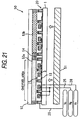
- FIG. 21 is a sectional view of the main part of a flat-panel display unit 50 of the embodiment.
- the light modulation elements 20 of the first embodiment are used as an example.
- An ultraviolet surface light source 51 used as an ultraviolet output section is disposed on the transparent substrate 1 side of the light modulation elements 20.
- a front panel 52 is placed above the light modulation elements 20 and fluorescent material 53a, 53b, ... are provided in a one-to-one correspondence with the light modulation elements on the light modulation element side of the front plate 52.
- a black matrix 54 is provided between the fluorescent material, improving the contrast of a display image.
- light from the ultraviolet surface light source 51 enters the transparent substrate 1 and is guided to the top face of the transparent substrate 1 in the light passing-through mode of the light modulation elements 20.
- the light from the light modulation elements 20 is applied to the fluorescent material 53a, 53b, ..., whereby the fluorescent material 53a, 53b, ... are excited for emitting light, forming any desired image.
- fluorescent material of the three primary colors may be placed in order for enabling a color image to be displayed or only single-color fluorescent material may be provided for displaying a monochrome image.
- the front plate is formed of glass, etc., but may be a fiber-like substrate or a diffusion film.
- the light modulation elements 20 of the flat-panel display unit 50 may be stabilized by deaerating the space between the transparent substrate 1 and the front panel 52 and then pouring a rare gas for sealing the whole for preventing the effect of disturbance.
- the needle 15 When the scan signal electrode 25 and the image signal electrode 29 are at the same potential, the needle 15 is positioned overlapping above the light modulation area (opening part) 13 and light from the surface light source is blocked by the needle 15 and the shield-property conductive film 3 and does not pass through to the top face of the transparent substrate 1.
- a latch voltage is applied to the latch signal electrode 28 at the end of the scan, whereby the needle 15 is latched to the shield-property conductive film 3 by an electrostatic suction force. Resultantly, when the pixel is not selected, if voltage of another pixel is applied, the transmission factor of the pixel is held intact and active matrix drive is enabled.
- the light emitted from the transparent substrate 1 side is directly applied to the fluorescent material for exciting the same, so that the light use efficiency can be improved.
- the fluorescent material emits scattered light, the viewing angle can be widened as compared with a liquid crystal display for allowing light to pass through by orientation control of liquid crystal molecules. Further, the fluorescent material can be easily put into an array, thus the manufacturing costs can be reduced.
- the needle 15 can be driven by the electromechanical operation, the drive voltage can be made low as compared with a plasma display, etc.; the drive voltage can also be made low by using a low elastic material, for example, a high polymer of polyimide, etc., as the material of the needle 15 or optimizing the shape of the needle 15.
- the light modulation elements 20 of the first embodiment are used as an example.
- the light modulation elements used with the flat-panel display unit 50 of the fourth embodiment are not limited to the light modulation elements 20; the light modulation elements 30, 35, 40 of the second and third embodiments can also be applied to the flat-panel display unit 50 of the fourth embodiment.
- the light modulation operation is performed by the first electromechanical force and the displacement state of the needle can be held or canceled in response to the second electromechanical force generated by the drive means.
- a memory property can be provided for the light transmission factor of the light modulation element and the element structure enabling active matrix drive can be provided.
- the array-type light modulation element comprises a plurality of parallel scan signal electrodes, a plurality of image signal electrodes orthogonal to the scan signal electrodes, and light modulation elements being placed at intersection points of the scan signal electrodes and the image signal electrodes, so that the displacement state of each needle is held or canceled by the signal of the scan signal electrode and the displacement state of each needle is changed by the signal of the image signal electrode.
- latch signal electrodes are provided, whereby the displacement state of each needle is held or canceled by the signal of the latch signal electrode, thus highly efficient and stable drive is enabled.
- the applied voltage or the voltage application timing is controlled, whereby the move distance of the needle can be changed and the light transmission factor of the light modulation element can be changed as desired.
- the modulated light by the light modulation element can be changed as binary gradation or in an analog manner for providing multiple levels of gray.
- the move state of the needle is held, whereby gradation can be provided with a memory property and active matrix drive can be provided.
- the flat-panel display unit uses the electrostatically driven light modulation elements, the light use efficiency can be improved and the viewing angle can be widened as compared with a liquid crystal display; moreover, the light modulation elements can be easily put into an array, thus the manufacturing costs can be reduced. Since the needle can be driven by the electromechanical operation, the drive voltage can be lowered. In addition, efficient matrix drive is enabled, so that high image quality can also be provided in a moving picture and matrix drive capable of performing the operation at high speed and producing high-contrast display is enabled.
Landscapes
- Physics & Mathematics (AREA)
- General Physics & Mathematics (AREA)
- Optics & Photonics (AREA)
- Mechanical Light Control Or Optical Switches (AREA)
Claims (25)
- Un élément de modulation de lumière de type réseau comprenant une multiplicité d'éléments de modulation de lumière, chaque élément de modulation de lumière ayant un substrat (1) incluant une zone de modulation de lumière (13), une aiguille (15) disposée verticalement au-dessus de la zone de modulation de lumière (13), et un moyen d'entraînement pour effectuer une opération électromécanique consistant à générer une première force électromécanique pour l'aiguille (15), afin de déplacer l'aiguille, pour changer ainsi un facteur de transmission de la lumière traversant la zone de modulation de lumière, cet élément de modulation de lumière comprenant :un moyen d'entraînement supplémentaire pour générer ou annuler une seconde force électromécanique pour l'aiguille (15) dans une direction différente de celle de la première force électromécanique, afin de maintenir ou d'annuler l'état de déplacement de l'aiguille (15), caractérisé en ce que l'élément comprend :une multiplicité d'électrodes de signal de balayage (25) parallèles, chaque électrode de signal de balayage recevant une tension de signal de balayage et générant ou annulant la seconde force électromécanique;une multiplicité d'électrodes de signal d'image (29) orthogonales aux électrodes de signal de balayage, chaque électrode de signal d'image recevant une tension de signal d'image et générant ou annulant la première force électromécanique; etles éléments de modulation de lumière étant placés à des points d'intersection des électrodes de signal de balayage et des électrodes de signal d'image, dans lequell'état de déplacement de chaque aiguille est maintenu ou annulé par un signal d'électrode de signal de balayage et l'état de déplacement de chaque aiguille est changé par un signal de l'électrode de signal d'image, et dans lequel les directions des première et seconde forces électromécaniques sont pratiquement orthogonales l'une à l'autre.
- L'élément de modulation de lumière de type réseau selon la revendication 1, comprenant
une multiplicité d'électrodes de signal de verrouillage qui sont placées côte à côte avec les électrodes de signal de balayage, chaque électrode de signal de verrouillage recevant une tension de signal de verrouillage et maintenant ou annulant la seconde force électromagnétique;
dans lequel la multiplicité d'électrodes de signal d'image sont orthogonales aux électrodes de signal de verrouillage, dans lequel
les éléments de modulation de lumière sont placés à des points d'intersection des électrodes de signal de balayage et des électrodes de signal de verrouillage et des électrodes de signal d'image, et dans lequel
l'état de déplacement de chaque aiguille est maintenu ou annulé par des signaux de l'électrode de signal de balayage et de l'électrode de signal de verrouillage. - L'élément de modulation de lumière selon la revendication 1 ou 2, dans lequel la force électromécanique est une force électrostatique produite par un champ électrique.
- L'élément de modulation de lumière selon la revendication 1 ou 2, dans lequel la force électromécanique est une force électromagnétique.
- L'élément de modulation de lumière selon la revendication 1, dans lequel la force électromécanique est une force produite par un effet de contrainte d'électrostriction.
- L'élément de modulation de lumière selon l'une quelconque des revendications 1 - 5, dans lequel la direction de la première force électromécanique est pratiquement horizontale et la direction de la seconde force électromécanique est pratiquement verticale.
- L'élément de modulation de lumière selon l'une quelconque des revendications 1 - 5, dans lequel la direction de la première force électromécanique est pratiquement verticale et la direction de la seconde force électromécanique est pratiquement horizontale.
- L'élément de modulation de lumière selon l'une quelconque des revendications 1 à 5, dans lequel l'aiguille est partiellement supportée du côté d'un substrat et a une conductivité électrique, et une première électrode fixée et une seconde électrode fixée sont placées face à l'aiguille, dans lequel l'aiguille est déplacée pratiquement horizontalement par rapport au substrat, sur la base d'une différence de potentiel occasionnée par l'application d'une tension à la première électrode fixée et à l'aiguille, ce qui change le facteur de transmission de lumière, et dans lequel l'état de déplacement de l'aiguille est maintenu ou annulé par l'application d'une tension à la seconde électrode fixée et à l'aiguille.
- L'élément de modulation de lumière selon l'une quelconque des revendications 1 à 5, dans lequel l'aiguille est partiellement supportée du côté d'un substrat et a une conductivité électrique, et une première électrode fixée et une seconde électrode fixée sont placées face à l'aiguille, dans lequel l'aiguille est déplacée pratiquement verticalement par rapport au substrat, sur la base d'une différence de potentiel occasionnée par l'application d'une tension à la première électrode fixée et à l'aiguille, ce qui a pour effet de changer le facteur de transmission de lumière, et dans lequel l'état de déplacement de l'aiguille est maintenu ou annulé par l'application d'une tension à la deuxième électrode fixée et à l'aiguille.
- L'élément de modulation de lumière selon l'une quelconque des revendications 1 à 5, dans lequel l'aiguille a une propriété d'arrêt de la lumière et est placée en un point intermédiaire sur un chemin de lumière, et le niveau d'arrêt de lumière dans le chemin de lumière est changé par un déplacement de l'aiguille.
- L'élément de modulation de lumière selon l'une quelconque des revendications 1 à 4, dans lequel le facteur de transmission de lumière de l'élément de modulation de lumière est changé sur la base de l'un quelconque d'un effet d'interférences, de l'effet optique de champ de proximité, de l'effet de diffraction ou de l'effet de déviation de lumière qui est produit lorsque l'aiguille est déplacée.
- L'élément de modulation de lumière selon l'une quelconque des revendications 1 à 5, dans lequel :l'aiguille est partiellement supportée sur un substrat transparent, qui est transparent vis-à-vis de la lumière à moduler, et elle a une propriété d'arrêt de lumière et une conductivité électrique;une première électrode fixée fait face à une première direction de l'aiguille et est établie comme une cloison sur un plan perpendiculaire au substrat transparent;une seconde électrode fixée fait face à une seconde direction de l'aiguille et est établie sur un plan parallèle au substrat transparent; etune pellicule d'arrêt de lumière est formée en laissant une ouverture en tant que zone de modulation de lumière, dans lequel
l'aiguille est déplacée dans la première direction par une force électrostatique produite par l'application d'une tension à l'aiguille et à la première électrode fixée, ce qui a pour effet de produire une modulation de lumière, et dans lequel l'aiguille est aspirée ou attirée dans la seconde direction par l'application d'une tension à l'aiguille et à la seconde électrode fixée, pour maintenir l'état de déplacement de l'aiguille, ou bien la force électrostatique est annulée pour annuler l'état de déplacement. - L'élément de modulation de lumière selon la revendication 13, dans lequel une multiplicité d'aiguilles et une multiplicité des premières électrodes fixées sont disposées sous la forme d'une grille.
- L'élément de modulation de lumière de type réseau selon l'une quelconque des revendications 1 à 13, dans lequel l'élément de modulation de lumière est dans un état d'arrêt de lumière lorsque l'aiguille n'est pas actionnée, et dans lequel un facteur de transmission de lumière augmente lorsque l'aiguille est déplacée par une force électrostatique, à partir de l'état d'arrêt de lumière.
- L'élément de modulation de lumière de type réseau selon l'une quelconque des revendications 1 à 13, dans lequel l'élément de modulation de lumière est dans un état de transmission complète de la lumière lorsque l'aiguille n'est pas actionnée, et dans lequel un facteur de transmission de lumière diminue lorsque l'aiguille est déplacée par une force électrostatique.
- Un procédé d'attaque d'un élément de modulation de lumière de type réseau selon l'une quelconque des revendications 1 à 15, ce procédé comprenant les étapes consistant à :dans une période de balayage d'écriture de l'élément de modulation de lumière, annuler le maintien de l'aiguille par un signal de balayage, ou un signal de balayage et un signal de verrouillage, et déplacer l'aiguille vers une position désirée quelconque, par un signal d'image; etdans une période de balayage de non-écriture, maintenir l'état de déplacement de l'aiguille par un signal de balayage, ou un signal de balayage et un signal de verrouillage.
- Le procédé d'attaque d'élément de modulation de lumière de type réseau selon la revendication 16, dans lequel l'aiguille est entraînée de manière binaire, avec deux positions en tant que destinations de déplacement.
- Le procédé d'attaque d'élément de modulation de lumière de type réseau selon la revendication 16, dans lequel l'aiguille est entraînée pour procurer de multiples niveaux de gris, avec des positions désirées quelconques en tant que destinations de déplacement.
- Le procédé d'attaque d'élément de modulation de lumière de type réseau selon la revendication 16, dans lequel la distance de déplacement de l'aiguille est fixée en réponse à un niveau de tension appliqué au signal d'image.
- Le procédé d'attaque d'élément de modulation de lumière de type réseau selon la revendication 18, dans lequel la distance de déplacement de l'aiguille est fixée en réponse au temps d'application de tension au signal d'image.
- Le procédé d'attaque d'élément de modulation de lumière de type réseau selon la revendication 19, dans lequel l'aiguille est entraînée avec une vitesse de réponse de déplacement, en réponse au niveau de tension appliqué au signal d'image.
- Le procédé d'attaque d'élément de modulation de lumière de type réseau selon la revendication 20, dans lequel l'aiguille est maintenue à une position à laquelle l'aiguille est sollicitée de façon élastique à l'instant de début de balayage d'écriture sur l'élément de modulation de lumière, dans lequel le maintien de l'aiguille est annulé après l'expiration d'un temps arbitraire, et dans lequel l'aiguille est à nouveau maintenue à la terminaison du balayage d'écriture.
- Le procédé d'attaque d'élément de modulation de lumière de type réseau selon la revendication 22, dans lequel la période au cours de laquelle l'aiguille est maintenue à la position à laquelle l'aiguille est sollicitée de façon élastique, est fixée de façon à être en chevauchement avec une période de balayage d'écriture sur une autre rangée.
- Une unité de visualisation à panneau plat, comprenant
l'élément de modulation de lumière de type réseau selon l'une quelconque des revendications 1 à 15,
une source de lumière de surface placée face à l'élément de modulation de lumière de type réseau, et
une substance fluorescente placée sur un côté opposé à la source de lumière de surface, avec l'élément de modulation de lumière de type réseau entre eux, dans laquelle :la lumière traversant l'élément de modulation de lumière de type réseau fait émettre de la lumière à la substance fluorescente pour produire une visualisation. - L'unité de visualisation à panneau plat selon la revendication 24, dans laquelle la lumière émise par la source de lumière est de la lumière ultraviolette.
Applications Claiming Priority (3)
| Application Number | Priority Date | Filing Date | Title |
|---|---|---|---|
| JP1204399 | 1999-01-20 | ||
| JP1204399A JPH11319809A (ja) | 1998-03-18 | 1999-01-20 | ダイオキシン類含有液の処理方法 |
| EP00101013A EP1022598B1 (fr) | 1999-01-20 | 2000-01-19 | Dispositif de modulation de la lumiére, sa méthode de commande, et dispositif d'affichage à panneau plat |
Related Parent Applications (1)
| Application Number | Title | Priority Date | Filing Date |
|---|---|---|---|
| EP00101013A Division EP1022598B1 (fr) | 1999-01-20 | 2000-01-19 | Dispositif de modulation de la lumiére, sa méthode de commande, et dispositif d'affichage à panneau plat |
Publications (2)
| Publication Number | Publication Date |
|---|---|
| EP1480068A1 EP1480068A1 (fr) | 2004-11-24 |
| EP1480068B1 true EP1480068B1 (fr) | 2006-05-03 |
Family
ID=36442001
Family Applications (1)
| Application Number | Title | Priority Date | Filing Date |
|---|---|---|---|
| EP04013886A Expired - Lifetime EP1480068B1 (fr) | 1999-01-20 | 2000-01-19 | Dispositif de modulation de la lumière du type réseau, sa méthode de commande, et dispositif d'affichage à panneau plat |
Country Status (2)
| Country | Link |
|---|---|
| EP (1) | EP1480068B1 (fr) |
| DE (1) | DE60027798T2 (fr) |
Family Cites Families (4)
| Publication number | Priority date | Publication date | Assignee | Title |
|---|---|---|---|---|
| EP0192702A1 (fr) * | 1984-08-21 | 1986-09-03 | SIMPSON, George, R. | Dispositifs binaires a volets, disposes en panneaux et actionnes electrostatiquement |
| US5062689A (en) * | 1990-08-21 | 1991-11-05 | Koehler Dale R | Electrostatically actuatable light modulating device |
| US6057814A (en) * | 1993-05-24 | 2000-05-02 | Display Science, Inc. | Electrostatic video display drive circuitry and displays incorporating same |
| AU5156198A (en) * | 1996-10-29 | 1998-05-22 | Xeotron Corporation | Optical device utilizing optical waveguides and mechanical light-switches |
-
2000
- 2000-01-19 DE DE2000627798 patent/DE60027798T2/de not_active Expired - Lifetime
- 2000-01-19 EP EP04013886A patent/EP1480068B1/fr not_active Expired - Lifetime
Also Published As
| Publication number | Publication date |
|---|---|
| DE60027798D1 (de) | 2006-06-08 |
| DE60027798T2 (de) | 2007-05-10 |
| EP1480068A1 (fr) | 2004-11-24 |
Similar Documents
| Publication | Publication Date | Title |
|---|---|---|
| EP1022598B1 (fr) | Dispositif de modulation de la lumiére, sa méthode de commande, et dispositif d'affichage à panneau plat | |
| US6288829B1 (en) | Light modulation element, array-type light modulation element, and flat-panel display unit | |
| US6239777B1 (en) | Display device | |
| JP3919954B2 (ja) | アレイ型光変調素子及び平面ディスプレイの駆動方法 | |
| JP3824290B2 (ja) | アレイ型光変調素子、アレイ型露光素子、及び平面型ディスプレイ、並びにアレイ型光変調素子の駆動方法 | |
| TWI253041B (en) | Area array modulation and lead reduction in interferometric modulators | |
| EP0545569B1 (fr) | Appareil pour adresser des éléments d'emmagasinage de données avec un gaz ionisable excité par une source AC d'énergie | |
| EP1055217B1 (fr) | Dispositif d'affichage comprenant un guide de lumiere dont les tensions d'electrode dependent des tensions d'electrodes precedemment appliquees | |
| JP2000098269A (ja) | アレイ型光変調素子及び平面ディスプレイの駆動方法 | |
| KR20040044975A (ko) | 유지 전극을 갖는 수직 스위칭 전기영동 디스플레이 | |
| HK1004350B (en) | Apparatus for addressing data storage elements with an ionizable gas excited by an ac energy source | |
| EP1647003A1 (fr) | Systeme de commande pour un affichage bistable a precision d'echelle de gris amelioree | |
| KR20070006727A (ko) | 전기 영동 디스플레이 패널 | |
| US20080165120A1 (en) | Passive Matrix Electrophoretic Display with Reset | |
| KR20090129760A (ko) | 전기영동 소자 | |
| JPH1195693A (ja) | 表示装置 | |
| JP2001201770A (ja) | 電気泳動表示装置およびその駆動方法 | |
| KR20090013786A (ko) | 개선된 디스플레이 디바이스 | |
| JP2002372701A (ja) | 画像表示装置 | |
| KR100412005B1 (ko) | 개선된dmd제어용다중바이어스레벨리셋파형을제공하는공간광변조기및그동작방법 | |
| KR101235627B1 (ko) | 디스플레이 장치 | |
| JP2001249366A (ja) | 電気泳動表示装置およびその駆動方法 | |
| KR101531379B1 (ko) | 입자들의 움직임을 사용하는 전자 디바이스 | |
| US8390546B2 (en) | Line-at-a-time foil display | |
| EP0614167B1 (fr) | Shunt d'électrodes dans un canal avec plasma |
Legal Events
| Date | Code | Title | Description |
|---|---|---|---|
| PUAI | Public reference made under article 153(3) epc to a published international application that has entered the european phase |
Free format text: ORIGINAL CODE: 0009012 |
|
| 17P | Request for examination filed |
Effective date: 20040614 |
|
| AC | Divisional application: reference to earlier application |
Ref document number: 1022598 Country of ref document: EP Kind code of ref document: P |
|
| AK | Designated contracting states |
Kind code of ref document: A1 Designated state(s): AT BE CH CY DE DK ES FI FR GB GR IE IT LI LU MC NL PT SE |
|
| AX | Request for extension of the european patent |
Extension state: AL LT LV MK |
|
| 17Q | First examination report despatched |
Effective date: 20050218 |
|
| AKX | Designation fees paid |
Designated state(s): DE FR GB |
|
| GRAP | Despatch of communication of intention to grant a patent |
Free format text: ORIGINAL CODE: EPIDOSNIGR1 |
|
| GRAS | Grant fee paid |
Free format text: ORIGINAL CODE: EPIDOSNIGR3 |
|
| GRAA | (expected) grant |
Free format text: ORIGINAL CODE: 0009210 |
|
| AC | Divisional application: reference to earlier application |
Ref document number: 1022598 Country of ref document: EP Kind code of ref document: P |
|
| AK | Designated contracting states |
Kind code of ref document: B1 Designated state(s): DE FR GB |
|
| REG | Reference to a national code |
Ref country code: GB Ref legal event code: FG4D |
|
| REF | Corresponds to: |
Ref document number: 60027798 Country of ref document: DE Date of ref document: 20060608 Kind code of ref document: P |
|
| ET | Fr: translation filed | ||
| PLBE | No opposition filed within time limit |
Free format text: ORIGINAL CODE: 0009261 |
|
| STAA | Information on the status of an ep patent application or granted ep patent |
Free format text: STATUS: NO OPPOSITION FILED WITHIN TIME LIMIT |
|
| RAP2 | Party data changed (patent owner data changed or rights of a patent transferred) |
Owner name: FUJIFILM CORPORATION |
|
| 26N | No opposition filed |
Effective date: 20070206 |
|
| REG | Reference to a national code |
Ref country code: GB Ref legal event code: 732E |
|
| REG | Reference to a national code |
Ref country code: FR Ref legal event code: TP Ref country code: FR Ref legal event code: CD |
|
| PGFP | Annual fee paid to national office [announced via postgrant information from national office to epo] |
Ref country code: DE Payment date: 20101222 Year of fee payment: 12 Ref country code: FR Payment date: 20110128 Year of fee payment: 12 |
|
| PGFP | Annual fee paid to national office [announced via postgrant information from national office to epo] |
Ref country code: GB Payment date: 20110119 Year of fee payment: 12 |
|
| GBPC | Gb: european patent ceased through non-payment of renewal fee |
Effective date: 20120119 |
|
| REG | Reference to a national code |
Ref country code: FR Ref legal event code: ST Effective date: 20120928 |
|
| PG25 | Lapsed in a contracting state [announced via postgrant information from national office to epo] |
Ref country code: GB Free format text: LAPSE BECAUSE OF NON-PAYMENT OF DUE FEES Effective date: 20120119 Ref country code: DE Free format text: LAPSE BECAUSE OF NON-PAYMENT OF DUE FEES Effective date: 20120801 |
|
| REG | Reference to a national code |
Ref country code: DE Ref legal event code: R119 Ref document number: 60027798 Country of ref document: DE Effective date: 20120801 |
|
| PG25 | Lapsed in a contracting state [announced via postgrant information from national office to epo] |
Ref country code: FR Free format text: LAPSE BECAUSE OF NON-PAYMENT OF DUE FEES Effective date: 20120131 |