JP3919954B2 - アレイ型光変調素子及び平面ディスプレイの駆動方法 - Google Patents
アレイ型光変調素子及び平面ディスプレイの駆動方法 Download PDFInfo
- Publication number
- JP3919954B2 JP3919954B2 JP29557098A JP29557098A JP3919954B2 JP 3919954 B2 JP3919954 B2 JP 3919954B2 JP 29557098 A JP29557098 A JP 29557098A JP 29557098 A JP29557098 A JP 29557098A JP 3919954 B2 JP3919954 B2 JP 3919954B2
- Authority
- JP
- Japan
- Prior art keywords
- electrode
- light
- light modulation
- modulation element
- voltage
- Prior art date
- Legal status (The legal status is an assumption and is not a legal conclusion. Google has not performed a legal analysis and makes no representation as to the accuracy of the status listed.)
- Expired - Fee Related
Links
Images










Classifications
-
- G—PHYSICS
- G09—EDUCATION; CRYPTOGRAPHY; DISPLAY; ADVERTISING; SEALS
- G09G—ARRANGEMENTS OR CIRCUITS FOR CONTROL OF INDICATING DEVICES USING STATIC MEANS TO PRESENT VARIABLE INFORMATION
- G09G3/00—Control arrangements or circuits, of interest only in connection with visual indicators other than cathode-ray tubes
- G09G3/20—Control arrangements or circuits, of interest only in connection with visual indicators other than cathode-ray tubes for presentation of an assembly of a number of characters, e.g. a page, by composing the assembly by combination of individual elements arranged in a matrix no fixed position being assigned to or needed to be assigned to the individual characters or partial characters
- G09G3/34—Control arrangements or circuits, of interest only in connection with visual indicators other than cathode-ray tubes for presentation of an assembly of a number of characters, e.g. a page, by composing the assembly by combination of individual elements arranged in a matrix no fixed position being assigned to or needed to be assigned to the individual characters or partial characters by control of light from an independent source
- G09G3/3433—Control arrangements or circuits, of interest only in connection with visual indicators other than cathode-ray tubes for presentation of an assembly of a number of characters, e.g. a page, by composing the assembly by combination of individual elements arranged in a matrix no fixed position being assigned to or needed to be assigned to the individual characters or partial characters by control of light from an independent source using light modulating elements actuated by an electric field and being other than liquid crystal devices and electrochromic devices
- G09G3/3466—Control arrangements or circuits, of interest only in connection with visual indicators other than cathode-ray tubes for presentation of an assembly of a number of characters, e.g. a page, by composing the assembly by combination of individual elements arranged in a matrix no fixed position being assigned to or needed to be assigned to the individual characters or partial characters by control of light from an independent source using light modulating elements actuated by an electric field and being other than liquid crystal devices and electrochromic devices based on interferometric effect
-
- G—PHYSICS
- G02—OPTICS
- G02B—OPTICAL ELEMENTS, SYSTEMS OR APPARATUS
- G02B26/00—Optical devices or arrangements for the control of light using movable or deformable optical elements
- G02B26/08—Optical devices or arrangements for the control of light using movable or deformable optical elements for controlling the direction of light
- G02B26/0875—Optical devices or arrangements for the control of light using movable or deformable optical elements for controlling the direction of light by means of one or more refracting elements
-
- G—PHYSICS
- G09—EDUCATION; CRYPTOGRAPHY; DISPLAY; ADVERTISING; SEALS
- G09G—ARRANGEMENTS OR CIRCUITS FOR CONTROL OF INDICATING DEVICES USING STATIC MEANS TO PRESENT VARIABLE INFORMATION
- G09G3/00—Control arrangements or circuits, of interest only in connection with visual indicators other than cathode-ray tubes
- G09G3/20—Control arrangements or circuits, of interest only in connection with visual indicators other than cathode-ray tubes for presentation of an assembly of a number of characters, e.g. a page, by composing the assembly by combination of individual elements arranged in a matrix no fixed position being assigned to or needed to be assigned to the individual characters or partial characters
- G09G3/34—Control arrangements or circuits, of interest only in connection with visual indicators other than cathode-ray tubes for presentation of an assembly of a number of characters, e.g. a page, by composing the assembly by combination of individual elements arranged in a matrix no fixed position being assigned to or needed to be assigned to the individual characters or partial characters by control of light from an independent source
- G09G3/3433—Control arrangements or circuits, of interest only in connection with visual indicators other than cathode-ray tubes for presentation of an assembly of a number of characters, e.g. a page, by composing the assembly by combination of individual elements arranged in a matrix no fixed position being assigned to or needed to be assigned to the individual characters or partial characters by control of light from an independent source using light modulating elements actuated by an electric field and being other than liquid crystal devices and electrochromic devices
-
- G—PHYSICS
- G09—EDUCATION; CRYPTOGRAPHY; DISPLAY; ADVERTISING; SEALS
- G09G—ARRANGEMENTS OR CIRCUITS FOR CONTROL OF INDICATING DEVICES USING STATIC MEANS TO PRESENT VARIABLE INFORMATION
- G09G3/00—Control arrangements or circuits, of interest only in connection with visual indicators other than cathode-ray tubes
- G09G3/20—Control arrangements or circuits, of interest only in connection with visual indicators other than cathode-ray tubes for presentation of an assembly of a number of characters, e.g. a page, by composing the assembly by combination of individual elements arranged in a matrix no fixed position being assigned to or needed to be assigned to the individual characters or partial characters
- G09G3/34—Control arrangements or circuits, of interest only in connection with visual indicators other than cathode-ray tubes for presentation of an assembly of a number of characters, e.g. a page, by composing the assembly by combination of individual elements arranged in a matrix no fixed position being assigned to or needed to be assigned to the individual characters or partial characters by control of light from an independent source
- G09G3/3433—Control arrangements or circuits, of interest only in connection with visual indicators other than cathode-ray tubes for presentation of an assembly of a number of characters, e.g. a page, by composing the assembly by combination of individual elements arranged in a matrix no fixed position being assigned to or needed to be assigned to the individual characters or partial characters by control of light from an independent source using light modulating elements actuated by an electric field and being other than liquid crystal devices and electrochromic devices
- G09G3/346—Control arrangements or circuits, of interest only in connection with visual indicators other than cathode-ray tubes for presentation of an assembly of a number of characters, e.g. a page, by composing the assembly by combination of individual elements arranged in a matrix no fixed position being assigned to or needed to be assigned to the individual characters or partial characters by control of light from an independent source using light modulating elements actuated by an electric field and being other than liquid crystal devices and electrochromic devices based on modulation of the reflection angle, e.g. micromirrors
-
- G—PHYSICS
- G09—EDUCATION; CRYPTOGRAPHY; DISPLAY; ADVERTISING; SEALS
- G09G—ARRANGEMENTS OR CIRCUITS FOR CONTROL OF INDICATING DEVICES USING STATIC MEANS TO PRESENT VARIABLE INFORMATION
- G09G3/00—Control arrangements or circuits, of interest only in connection with visual indicators other than cathode-ray tubes
- G09G3/20—Control arrangements or circuits, of interest only in connection with visual indicators other than cathode-ray tubes for presentation of an assembly of a number of characters, e.g. a page, by composing the assembly by combination of individual elements arranged in a matrix no fixed position being assigned to or needed to be assigned to the individual characters or partial characters
- G09G3/34—Control arrangements or circuits, of interest only in connection with visual indicators other than cathode-ray tubes for presentation of an assembly of a number of characters, e.g. a page, by composing the assembly by combination of individual elements arranged in a matrix no fixed position being assigned to or needed to be assigned to the individual characters or partial characters by control of light from an independent source
- G09G3/3433—Control arrangements or circuits, of interest only in connection with visual indicators other than cathode-ray tubes for presentation of an assembly of a number of characters, e.g. a page, by composing the assembly by combination of individual elements arranged in a matrix no fixed position being assigned to or needed to be assigned to the individual characters or partial characters by control of light from an independent source using light modulating elements actuated by an electric field and being other than liquid crystal devices and electrochromic devices
- G09G3/3473—Control arrangements or circuits, of interest only in connection with visual indicators other than cathode-ray tubes for presentation of an assembly of a number of characters, e.g. a page, by composing the assembly by combination of individual elements arranged in a matrix no fixed position being assigned to or needed to be assigned to the individual characters or partial characters by control of light from an independent source using light modulating elements actuated by an electric field and being other than liquid crystal devices and electrochromic devices based on light coupled out of a light guide, e.g. due to scattering, by contracting the light guide with external means
-
- G—PHYSICS
- G09—EDUCATION; CRYPTOGRAPHY; DISPLAY; ADVERTISING; SEALS
- G09G—ARRANGEMENTS OR CIRCUITS FOR CONTROL OF INDICATING DEVICES USING STATIC MEANS TO PRESENT VARIABLE INFORMATION
- G09G2300/00—Aspects of the constitution of display devices
- G09G2300/04—Structural and physical details of display devices
- G09G2300/0469—Details of the physics of pixel operation
- G09G2300/0473—Use of light emitting or modulating elements having two or more stable states when no power is applied
-
- G—PHYSICS
- G09—EDUCATION; CRYPTOGRAPHY; DISPLAY; ADVERTISING; SEALS
- G09G—ARRANGEMENTS OR CIRCUITS FOR CONTROL OF INDICATING DEVICES USING STATIC MEANS TO PRESENT VARIABLE INFORMATION
- G09G2300/00—Aspects of the constitution of display devices
- G09G2300/06—Passive matrix structure, i.e. with direct application of both column and row voltages to the light emitting or modulating elements, other than LCD or OLED
-
- G—PHYSICS
- G09—EDUCATION; CRYPTOGRAPHY; DISPLAY; ADVERTISING; SEALS
- G09G—ARRANGEMENTS OR CIRCUITS FOR CONTROL OF INDICATING DEVICES USING STATIC MEANS TO PRESENT VARIABLE INFORMATION
- G09G2300/00—Aspects of the constitution of display devices
- G09G2300/08—Active matrix structure, i.e. with use of active elements, inclusive of non-linear two terminal elements, in the pixels together with light emitting or modulating elements
-
- G—PHYSICS
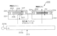
- G09—EDUCATION; CRYPTOGRAPHY; DISPLAY; ADVERTISING; SEALS
- G09G—ARRANGEMENTS OR CIRCUITS FOR CONTROL OF INDICATING DEVICES USING STATIC MEANS TO PRESENT VARIABLE INFORMATION
- G09G2310/00—Command of the display device
- G09G2310/02—Addressing, scanning or driving the display screen or processing steps related thereto
- G09G2310/0243—Details of the generation of driving signals
- G09G2310/0251—Precharge or discharge of pixel before applying new pixel voltage
-
- G—PHYSICS
- G09—EDUCATION; CRYPTOGRAPHY; DISPLAY; ADVERTISING; SEALS
- G09G—ARRANGEMENTS OR CIRCUITS FOR CONTROL OF INDICATING DEVICES USING STATIC MEANS TO PRESENT VARIABLE INFORMATION
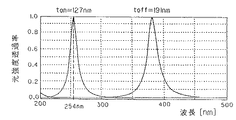
- G09G2310/00—Command of the display device
- G09G2310/02—Addressing, scanning or driving the display screen or processing steps related thereto
- G09G2310/0243—Details of the generation of driving signals
- G09G2310/0254—Control of polarity reversal in general, other than for liquid crystal displays
Landscapes
- Engineering & Computer Science (AREA)
- Physics & Mathematics (AREA)
- General Physics & Mathematics (AREA)
- Computer Hardware Design (AREA)
- Theoretical Computer Science (AREA)
- Optics & Photonics (AREA)
- Mechanical Light Control Or Optical Switches (AREA)
- Control Of Indicators Other Than Cathode Ray Tubes (AREA)
- Devices For Indicating Variable Information By Combining Individual Elements (AREA)
Description
【発明の属する技術分野】
本発明は、マイクロマシニングにより作製され、電気機械動作により光の透過率を変化させるアレイ型光変調素子、及び該アレイ型光変調素子を用いた平面ディスプレイの駆動方法に関し、特に、アレイ型光変調素子及び平面ディスプレイの交流駆動に関するものである。
【0002】
【従来の技術】
マイクロマシニングにより作製された可撓薄膜を、静電気力により機械的動作させることで光変調を行う電気機械的な光変調素子が知られている。この光変調素子としては、例えば、透明な電極とダイヤフラムからなる可撓薄膜を、支持部を介して導光板上の固定電極に架設したものがある。
この光変調素子では、両電極間に所定の電圧を印加することで電極間に静電気力を発生させ、可撓薄膜を固定電極に向かって撓ませる。これに伴って素子自体の光学的特性が変化して、光変調素子に光が透過する。一方、印加電圧をゼロにすることで可撓薄膜が弾性復帰し、光変調素子は光を遮光する。このようにして光変調が行なわれる。
【0003】
ところで、可撓薄膜を静電気力によって変形させたり弾性復帰させる場合、印加電圧Vgsと可撓薄膜の変位の関係はヒステリシス特性を示す。従って、印加電圧Vgsと光透過率Tとの関係も図30に示すようにヒステリシス特性を示すことになる。
このヒステリシス特性によれば、光変調要素がOFF(光遮蔽)状態の状態では、VgsがVth(L)以下ではOFF状態を維持し、VgsがVth(H)以上になるとON状態を維持する。そして、光変調要素は、VgsがVth(H)以上ではON状態を維持したままとなり、Vs(L)以下となるとOFF状態に飽和する。尚、Vgsの極性が負の場合は、正極性の縦軸対称の特性となる。
【0004】
【発明が解決しようとする課題】
しかしながら、上記従来例においては、以上のような特性を利用して変調要素を2次元に配置して、マトリクス駆動を行うことにより2次元の光変調素子を構成できるが、マトリクス駆動には単純マトリクスとアクティブマトリクス駆動があって、何れの駆動方法においても先述の変調要素の特性から、変調要素に印加する電圧は片方の極性で駆動可能であり、変調要素には直流電圧成分が印加される。
ところが、直流成分が加わる駆動では、可撓薄膜の内部を絶縁体で構成すると、電極−絶縁体−電極構造という構造において、絶縁体のマイグレーションによる絶縁不良、あるいは空間電荷の発生/トラップにより寄生の内部電界等が発生して動作が不安定になる可能性がある。液晶等では直流成分が加わる駆動の不安定さを避けるために交流駆動方式が行われているが、特に、絶縁体が高分子等で構成する場合に不安定な状態になる可能性が大きいという問題があった。
【0005】
本発明は、このような従来の問題点に鑑みてなされたもので、変調要素への印加電圧波形を交流駆動による駆動波形とすることによって、絶縁体のマイグレーションによる絶縁不良や空間電荷の発生を防止して、安定動作可能なアレイ型光変調素子及び平面ディスプレイの駆動方法を提供することを目的としている。
【0006】
【課題を解決するための手段】
上記目的を達成するため、請求項1記載のアレイ型光変調素子の駆動方法は、静電気力による可撓部の変位動作と、該可撓部の弾性復帰動作により光変調を行う電気機械的な光変調素子を2次元の単純マトリクス構造状に配列して走査電極信号に従い各画素を選択し、画素電極にデータ信号を与えて駆動するアレイ型光変調素子の駆動方法において、前記光変調素子は、前記可撓部側の電極と固定側の電極とが絶縁体部材を介して当接するものであり、前記光変調素子の電極に直流成分を含まない交流信号を印加して、単純マトリクス駆動に基づく交流駆動を行うに際し、前記走査駆動信号の基本周期を奇数フレームと偶数フレームに分割し、前記奇数フレームと偶数フレームでは、前記走査電極および信号電極に印加される電圧を同じ極性として駆動信号の極性を反転するとともに、前記偶数フレームの走査電極および信号電極に印加される電圧V even を、前記光変調素子のON状態、OFF状態を維持するために最小限必要な印加電圧V max と奇数フレームの走査電極および信号電極に印加される電圧V odd との差に設定することを特徴とする。
【0007】
このアレイ型光変調素子の駆動方法では、直流成分を含まない交流駆動とすることで、直流成分が加わる駆動に付随する絶縁体のマイグレーションによる絶縁不良、内部電界の発生による動作の不安定さを解消することができる。そして、単純マトリクス駆動で、n行×m列の単純マトリクス構成の光変調素子を交流駆動することができる。
また、奇数フレームの駆動信号を、例えば、正極性とし、偶数フレームの駆動信号を負極性とすれば、1フレーム周期のトータルで変調素子への印加電圧は交流駆動となり平衡性を保持することができる。
そして、1周期間の奇数フレームの駆動電圧に対して、偶数フレームの駆動電圧の極性を反転させて交流駆動を行うことができる。
【0018】
請求項2記載の平面ディスプレイの駆動方法は、前記アレイ型光変調素子と、該アレイ型光変調素子に対向配置した平面光源と、アレイ型光変調素子を挟み前記平面光源の反対側に配設した蛍光体と、を備え、前記アレイ型光変調素子を請求項1記載の駆動方法により、前記アレイ型光変調素子から出射される光によって蛍光体を発光表示させることを特徴とする。
【0019】
この平面ディスプレイの駆動方法では、電気機械的なアレイ型光変調素子を交流駆動として、アレイ型光変調素子を通過した光源光により蛍光体を発光表示させる構成としているので、平面ディスプレイを安定、高精細に駆動することが可能になる。
【0020】
請求項3記載の平面ディスプレイの駆動方法は、前記平面光源が、前記蛍光体を励起させる紫外線出射光源であることを特徴とする。
【0021】
この平面ディスプレイの駆動方法では、平面光源からの出射紫外線光を光変調素子で透過、遮光して蛍光体を発光励起させることができる。
【0022】
【発明の実施の形態】
以下、本発明の実施の形態について図を参照して説明する。
図1は本発明の第1実施形態に係る光変調素子の構成図で、図2は図1に示す光変調素子の印加電圧と光透過率の特性を示す図で、図3は図1に示す光変調素子を2次元配列したアレイ型光変調素子の平面図である。
【0023】
可撓薄膜を電気機械動作させて光変調させる動作原理としては、可撓薄膜と透明な信号電極とを離反又は接触させることによる導光拡散作用(以下、導光拡散と称する。)を利用することができる。導光拡散では、空隙を光の透過抵抗として、空隙が形成されている際には、信号電極からの出射光を遮断もしくは減衰させる一方、可撓薄膜を信号電極に接触させた時のみに、信号電極からの出射光を可撓薄膜へ導光(モード結合)させ、その光を可撓薄膜において拡散させることで、可撓薄膜からの出射光の強度を制御する(光変調する)。
【0024】
図1に示すように、導光板1上には、紫外線に対して透明な一方の電極(信号電極)2を形成してある。この例としては、電子密度の高いITO等の金属酸化物、非常に薄い金属薄膜(アルミ等)、金属微粒子を透明絶縁体に分散した薄膜、又は高濃度ドープしたワイドハンドギャップ半導体等が好適である。
【0025】
電極2の上には、絶縁性の支持部3を形成してある。支持部3には、例えばシリコン酸化物、シリコン窒化物、セラミック、樹脂等を用いることができる。支持部3の上端面には、ダイヤフラム4を形成してある。電極2とダイヤフラム4との間には、空隙(キャビティ)5が形成されている。このダイヤフラム4には、ポリシリコン等の半導体、絶縁性のシリコン酸化物、シリコン窒化物、セラミック、樹脂等を用いることができる。また、ダイヤフラム4の屈折率は、導光板1の屈折率と同等かそれ以上が好ましい。
【0026】
ダイヤフラム4の上には、光拡散層6、例えば、無機、有機透明材料の表面に凹凸を形成したもの、マイクロプリズム、マイクロレンズを形成したものや、無機、有機多孔質材料、又は屈折率の異なる微粒子を透明基材に分散したもの等を形成してある。
【0027】
光拡散層6の上には、紫外線に対して透明な他方の電極(走査電極)7を形成してある。例として電極2と同様の材料のものを用いることができる。これらダイヤフラム4、光拡散層6、電極7は、可撓部としての可撓薄膜8を構成している。
【0028】
導光板1とダイヤフラム4との間には空隙5が存在するが、この空隙5は支持部3の高さで略決定される。空隙5の高さは、例えば、0.1μmから10μm程度が好ましい。この空隙5は、通常、犠牲層のエッチングにより形成される。
【0029】
また、上述の構成例の他に、ダイヤフラム4と光拡散層6とを同一の材料で構成しても良い。例えば、窒化シリコン膜でダイヤフラム4を構成し、上面側の表面に凹凸を形成することによって、拡散機能を持たせることができる。
【0030】
次に、このように構成した光変調素子10の動作原理を説明する。
電圧OFF時、両電極2、7の電圧がゼロで、ダイヤフラム4と導光板1との間に空隙5(例:空気)が存在する場合、導光板1の屈折率をnwとすると、空気との界面における全反射臨界角θcは
θc=sin-1(nw)
となる。従って、紫外線は、界面への入射角θが、θ>θcのとき、図1(a)に示すように、導光板1内を全反射しながら進む。
【0031】
電圧ON時、両電極2、7に電圧を印加し、ダイヤフラム4と導光板1表面とを接触又は十分な距離に近づけた場合、図1(b)に示すように、紫外線は、ダイヤフラム4側に伝搬透過し、更に、光拡散層6により拡散されて表面側に出射する。
【0032】
この実施形態による光変調素子10によれば、電圧印加によるダイヤフラム4の位置制御により、光変調を行うことができる。
尚、導光板1とダイヤフラム4の間には紫外線に対して透明な電極2が存在するが、通常使用される薄膜の厚さ(2000Å)程度であれば、上述の動作上問題の生ずることはない。
【0033】
また、可撓薄膜8を静電気応力により変形/弾性復帰させる場合、印加電圧Vgsと可撓薄膜の変位の関係はヒステリシス特性を示す。従って、印加電圧Vgsと光透過率Tの関係も図2に示すようなヒステリシス特性を示す。
【0034】
ヒステリシス特性は、変調要素(光変調素子)がOFF(光遮蔽)状態では、Vgsが0V〜Vth(L)ではOFF状態を維持する。VgsがVs(H)以上になるとON状態に飽和する。その後、VgsがVth(H)以上ではON状態を維持する。さらに、Vgsが0V〜Vs(L)となるとOFF状態に飽和する。
尚、このヒステリシス特性はVgsの極性に対して縦軸対称の特性となる。本実施形態では、Vgsの極性が負の場合には図2の左側のヒステリシスループとなり、正の場合には右側のヒステリシスループとなるため、左側のヒステリシスループを偶数フレーム用のヒステリシス特性、右側のヒステリシスループを奇数フレーム用のヒステリシス特性として用いている。また、この逆であっても良い。
【0035】
以上、詳述した導光板による光変調部以外にも、後述のような薄膜を静電気力により変形、移動させて光変調を行う型等あっても同様なヒステリシス特性となり、同様に極性の正負を偶数フレーム、奇数フレームに対応させて用いることができる。
【0036】
本実施の形態では、図3に示すように、光変調素子10がn行×m列の2次元マトリクス状に配列される。即ち、マトリクスの各交点Tr(1,1)、Tr(1,2)、Tr(2,1)、Tr(2,2)には光変調素子10がそれぞれ配置され、アレイ型光変調素子50を構成する。
各光変調素子10は、一画素の領域に対応させてある。尚、ここではマトリクスの一部である図3の2行2列のマトリクスに着目して説明することにする。
尚、このアレイ型光変調素子50は、単純マトリクス駆動により動作する。
【0037】
同じ行に配列された光変調素子10の一方のそれぞれの電極は、共通に接続して走査電極7としてある。この走査電極には電位Vgが印加される。又、同じ行に配列された光変調素子10のそれぞれの電極は、共通に接続して信号電極2としてある。この信号電極には電位Vbが印加される。従って、各光変調素子10に印加される電極間電圧VgsはVb−Vgとなる。
【0038】
アレイ型光変調素子50を駆動するには、走査信号に従って、行順次に走査電極7を走査し、これと同期させて、走査された電極7に対応するデータ信号を信号電極2に印加する。
【0039】
ここで、走査電極7には、リセット信号、選択信号、非選択信号の三種類の信号(電圧)が与えられる。
リセット信号は、光変調素子10の以前の状態や信号電極電圧に拘わらず、その行の光変調素子10をOFF(光遮蔽)にする。この時の走査電極の電圧をVg(r)とする。
【0040】
選択信号は、その行にデータを書き込むための信号(書き込み動作用の信号)である。この信号と同時に、信号電極に印加された電圧に従い、光変調素子10の状態がON(光透過)又はOFF(光遮蔽)に決定される。この時の走査電極の電圧をVg(s)とする。
【0041】
非選択信号は、選択がなされないときの信号である。この時、信号電極の電圧に拘わることなく光変調素子10の状態は変わらず、前の状態が維持される。この時の走査電極の電圧をVg(ns) とする。
【0042】
一方、信号電極2には、ON信号、OFF信号の二種類の信号(電圧)が与えられる。
ON信号は、選択された行の光変調素子10に対し、光変調素子10の状態をON(光透過)にする。この時の信号電極2の電圧をVb(on) とする。
【0043】
OFF信号は、選択された行の光変調素子10に対し、光変調素子10の状態をOFF(光遮蔽)にする。但し、実際には、直前で光変調素子10がリセットされることを想定しているので、光変調素子10の状態をOFF(光遮蔽)にする場合は、前の状態(OFF状態)を維持する信号でよい。この時の信号電極2の電圧をVb(off)とする。
【0044】
以上の走査電極電圧、信号電極電圧の組み合わせにより、光変調素子10の電極間電圧Vgsは、以下の6種類の電圧に分けられる。また、電極間電圧Vgsと透過率のヒステリシス特性により、特定の条件が与えられることになる。
【0045】
Vgs(r-on) =Vb(on) −Vg(r) ≦ Vs(L)
Vgs(r-off) =Vb(off)−Vg(r) ≦ Vs(L)
Vgs(s-on) =Vb(on) −Vg(s) ≧ Vs(H)
Vgs(s-off) =Vb(off)−Vg(s) ≦ Vth(L)
Vgs(ns-on) =Vb(on) −Vg(ns) ≦ Vth(L)
Vgs(ns-off)=Vb(off)−Vg(ns) ≧ Vth(H)
【0046】
以上の条件をまとめると、図4の奇数フレーム相当の図に示す通りになる。 例えば、走査電極電圧Vg がリセットVg(r)で、信号電極電圧Vb がON即ちVb(on) の場合にはVs(H)より大きい値の信号電極電圧Vb (図中太実線61)から、Vs(H)とVth(L) との間の値の走査電極電圧Vg (図中太実線63)が減算され、その値(図中太実線65)がVs(L)より小さくなる。即ち、
Vgs(r-on)≦Vs(L)
となる。その他同様にして、6種類の電圧が定まることになる。
また、基本周期(1フレーム)毎に変調要素の電極間電圧Vgsの交流化を行うために、図5には反転極性の偶数フレームの場合を示し、それぞれ図4、図5の表には奇数フレームの場合と偶数フレームの場合の2通りを示している。
偶数フレームについては、電極間印加電圧Vgsの極性を反転させるために、奇数フレームのVgとVbによる印加電圧Voddは、偶数フレームのVgとVbによる印加電圧Vevenに対して、各々次式となるようにする。
Veven=Vmax−Vodd
ここで、Vmaxは印加電圧の最大値である。
【0047】
次に、このような電極間電圧Vgsと透過率との関係を利用して、光変調素子10を2次元に配置したマトリクスにデータを書き込む方法を説明する。
マトリクスとして図3に示した2行2列のマトリクスを用い、データの書き込みを行う。マトリクスの各光変調素子10には、以下のON、OFFデータを書き込むものとする。
Tr(1,1) → ON Tr(1,2) → OFF
Tr(2,1) → OFF Tr(2,2) → ON
【0048】
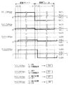
マトリクスには、図6に示すような波形の電圧を印加する。
例えば、奇数フレーム、偶数フレームの1行目Vg(1)には、
t1:リセット電圧 t2:選択電圧
t3:非選択電圧 t4:非選択電圧
を印加する。
1列目Vb(1)には、
t1:don't care t2:ON電圧
t3:OFF電圧 t4:don't care
を印加する。
これにより、図7に示すように、各光変調素子10に所望のデータが行順次で書き込まれる。
そして、光変調素子のリセット走査の後に、該素子の変位動作又は状態維持を選択する書き込み走査を行うことで、素子のヒステリシス特性により書き込み走査前の状態が次の動作に影響を及ぼすことが防止され、安定した書き込み走査を行うことができる。また、素子のヒステリシス特性により、単純マトリクス構成の二次元光変調アレイを矛盾なく、即ち、非選択走査ライン上の画素が書き込み走査時に設定されたON/OFF状態を確実に維持されるように駆動することが可能となる。
【0049】
例えば上述の1行1列目のマトリクスTr(1,1)の場合では、
Vgs=Vb(1)−Vg(1)であるから、奇数フレーム、偶数フレームで、
t1:リセット電圧(OFF) t2:ON
t3:状態維持 t4:状態維持
となる。
【0050】
従って、t2におけるONの状態が維持(メモリー)され、その結果、マトリクスTr(1,1)は光変調素子10が「ON」の状態となる。その他、同様にして、他のマトリクスTr(1,2)は「OFF」、Tr(2,1)は「OFF」、Tr(2,2)は「ON」の状態となる。
【0051】
以上の動作により、図6に示す奇数フレーム及び偶数フレームのVg、Vb印加電圧により、変調要素の印加電圧Vgsは、図7に示すように、1フレーム(基本周期)毎に奇数フレームと偶数フレームは0Vを中心に交流化され、直流成分が無くなり、単純マトリクスの交流駆動が行われ、確実な動作を実現しつつアレイ型光変調素子の大型化、高精細化を図ることができる。
【0052】
次に、本発明の第2実施形態について図面を参照して詳細に説明する。
本実施形態は、アクティブマトリクス構造に対し交流駆動を取り入れたものである。
まず、アレイ型光変調素子を半導体スイッチによりアクティブ駆動させる場合を説明する。
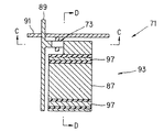
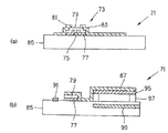
図8は本実施形態の光変調部の平面図で、図9は図8のC−C及びD−D断面図で、図10は図8に示した画素部の等価回路図である。
【0053】
図8〜図10に示すように、アレイ型光変調素子71は、画素毎に能動素子(例として、TFT)73を設けてある。TFT73は図9(a)及び図10に示すようにゲート電極75、絶縁膜77、a−Si:H層79、ドレイン電極81、ソース電極83から構成される。また、このTFT73は、基板85上に形成される。
【0054】
TFT73のソース電極83には図9(b)及び図10に示すように、画素電極87が接続される。ドレイン電極81には、列毎の画像信号ライン89が接続される。ゲート電極75には、行毎の走査信号ライン91が接続される。
【0055】
画素電極87は、光変調部93にある可撓薄膜95の上部に積層される。可撓薄膜95は、支柱97に架橋される。また、画素電極87と対向して、基板85には共通電極99が設けられ、電位Vcomが印加される。
【0056】
このように構成されたアレイ型光変調素子71の動作について説明する。
図10は半導体トランジスタによる画素部の等価回路図であり、光変調部93では、ゲート電極75に接続された走査信号ライン91にTFT73を導通させる電圧Vg-onが印加される。そして、ドレイン電極81に接続された画像信号ライン89に所望の画像信号電圧Vb が印加されると、ドレイン電極81とソース電極83とが導通する。従って、画像信号電圧が、画素電極87に印加されることになる。これにより、共通電極99の電位Vcom と画素電極87の電位との電圧Vgs=(Vb −Vcom )により静電気応力が働き、所望の光変調を行う。
この後に他の行の走査のため、TFT73が非導通となっても上述の光変調状態は維持され、複数の行のマトリクス変調が可能となる。
【0057】
図11に示すn行×m列のアクティブマトリクスの構成例では、走査信号ライン91に順次走査電圧を印加し、これに接続されているTFT73を一斉にオン状態とする。同時に、画像信号ライン89から画像信号電圧Vb を印加し、TFT73を通して各画素の静電容量に電荷を蓄積する。1行の走査が終了すると、TFT73はオフ状態となり、画素容量に蓄積された電荷はそのまま保持されることになる。
【0058】
次に、本実施形態のアクティブマトリクス素子を機械的導電スイッチ型で構成した例を示す。
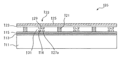
図12は図11で示した半導体スイッチを機械的導電スイッチで構成したアクティブマトリクス素子の平面図であり、図13は図12のA−A断面図、図14は図12のB−B断面図である。
【0059】
基板111上には、ストライプ状の複数の平行な走査信号共通電極113(第1走査電極)を形成してある。基板111上には、少なくともこの走査信号共通電極113を覆う絶縁層115を形成してある。また、基板111上には、走査信号共通電極113に直交するストライプ状の複数の平行なデータ信号電極116を形成してある。基板111上の走査信号共通電極113とデータ信号電極116とに包囲された四角形状の領域には、画素部共通電極117及び光機能素子119を順次積層してある。
【0060】
走査信号共通電極113に沿ってストライプ状に形成された絶縁層115上には、複数の支持部121を絶縁層115の長手方向に沿って、等間隔で設けてある。支持部121の上端部には、ストライプ状の可撓薄膜123及び走査信号電極125(第2走査電極)を順次積層して架設してある。可撓薄膜123は、絶縁材料からなる。この可撓薄膜123と走査信号電極125とは、支持部121に架設されることで、間隙を挟んで、絶縁層115に被覆された走査信号共通電極113と対向している。走査信号電極125とデータ信号電極116とは、複数の交差部126(図12参照)を有するマトリクス状に配設されている。
尚、支持部121は、上記のように個別に設けることなく、例えば中空薄膜の端部を固定する等の他の形成方法により構成してもよい。
【0061】
光機能素子119の上面には、画素部共通電極117とで光機能素子119を挟む画素電極127を形成してある。絶縁層115上のデータ信号電極116の近傍には、この画素電極127の一部分127a(図12を参照)を延設してある。データ信号電極116と、この画素電極127の一部分127aとは、図13に示すように同一高さで、且つ間隙を隔てて平行に配設してある。つまり、非導通状態に配設されている。
【0062】
可撓薄膜123の下面には、金属等からなる導電膜129を形成してある。導電膜129は、アルミ、銅、銀、金等を用いることができる。導電膜129は、データ信号電極116及び画素電極127に空隙131を介して対向している。可撓薄膜123、データ信号電極116、画素電極127、導電膜129は、マトリクス駆動手段である機械的導電スイッチ133を構成している。機械的導電スイッチ133は、マトリクス状に配設されたデータ信号電極116と走査信号電極125との各交差部126に設けられている。
【0063】
図15は図12に示すアクティブマトリクス素子の動作状態を示す説明図である。
このように構成されたアクティブマトリクス素子135では、図15(a)に示すように、走査信号共通電極113に対して、走査信号電極125が同電位であると、可撓薄膜123は静電気力を受けず撓まない。従って、データ信号電極116と画素電極127aとは、電気的に接触することなく非導通状態を保つ。
【0064】
一方、図15(b)に示すように、走査信号共通電極113に対して、走査信号電極125に電圧を印加すると、可撓薄膜123が静電気力によって基板111側に撓み、可撓薄膜123の下方に位置するデータ信号電極116及び画素電極127aに導電膜129が電気的に接触する。これにより、データ信号電極116と画素電極127aとの電位が等しくなる。
【0065】
また、走査信号電極125の電圧をゼロにすると、可撓薄膜123は弾性力により元の位置に復帰して、データ信号電極116及び画素電極127aから離れる。これにより、図15(a)に示す状態となって、データ信号電極116と画素電極127とは、再び非導通状態となる。
【0066】
図16は図12に示すアクティブマトリクス素子のマトリクス動作の説明図である。
図16に示すマトリクスの場合では、可撓薄膜123を撓める電圧Vg-onを印加した走査信号電極125の画素電極127が、データ信号電極116と導通する。これにより、データ信号電極116と画素電極127との電位が等しくなる。また、その他の走査信号電極の画素電極は、それぞれ電気的に独立の電位で保持されることになる。
【0067】
図17は機械的スイッチによるアクティブマトリクス素子の等価回路図である。
図17も第2実施形態を構成するn行×m列のアクティブマトリクスに対する機械的スイッチによる構成例である。
この動作は図16の場合と同様に、走査信号VgのON/OFFに同期して、機械的スイッチを介して画素信号Vbが電極間に印加され駆動される。
【0068】
図18は以上のアクティブマトリクスにおける可撓薄膜のスイッチ特性を示すヒステリシス線図である。
走査信号共通電極113に対する走査信号電極125の電圧をVg とすると、可撓薄膜123によるスイッチ特性は、図18に示すようなヒステリシス特性を有する。即ち、Vg がVg-on以上になると導通(ON)し、Vg-off 以下になると非導通(OFF)になる。
【0069】
次に、上記アクティブマトリクス構成による交流駆動の動作を説明する。
図19は半導体スイッチ、機械スイッチ等によるn行×m列のアクティブマトリクス構成を示す図である。
図19において、各画素電極の電位をVp、共通電極の電位をVcomとすると、光変調素子の印加電圧Vgsは、Vgs=Vp−Vcom、となる。
【0070】
いま、図19のような2行2列の各画素に対し、以下の2値のデータを書き込む場合のアクティブマトリクス構成の交流駆動に付いて説明する。
Tr(1、1)→ON Tr(1、2)→OFF
Tr(2、1)→OFF Tr(2、2)→ON
図20は図19に示すアクティブマトリクス構成の交流駆動の電圧Vg、Vbを示す図である。
【0071】
この場合の印加電圧は、図20に示すように、奇数フレーム、偶数フレーム共に、
1行目Vg
t1:走査ON (導通)
t2:走査OFF(非導通)
2行目Vg
t1:走査OFF(非導通)
t2:走査ON (導通)
1列目Vb
t1:Tr(1、1)へON (透過)電圧印加
t2:Tr(2、1)へOFF(遮光)電圧印加
2列目Vb
t1:Tr(1、2)へOFF(遮光)電圧印加
t2:Tr(2、2)へON (透過)電圧印加
となる。
【0072】
このように走査ゲート電極を行順次でVg−onによりON(導通)にし、それと同期させてデータ信号電極からON(透過)又はOFF(遮光)の電位を供給する。その後、走査ゲート電極をOFF(非導通)にしても、画素電位の電位は保持される。
【0073】
また、走査ゲート電極からの供給される電圧はVg−onとVg−offだけであるが、データ信号電極から供給される電圧(Vp又はVb)は図20に示すように、
奇数フレーム時、ON の場合はV1
OFFの場合はV2
偶数フレーム時、ON の場合はV3
OFFの場合はV4
とする。ただし、
V1=Vcom+Vs(H)
V2=Vcom+Vs(L)
V3=Vcom−Vs(L)
V4=Vcom−Vs(H)
である。
【0074】
図21は図20に示すアクティブマトリクス構成の交流駆動により光変調素子に印加される電圧Vgsを示す図である。
先の図20に示した電圧印加による各画素のVgsは、図21に示すように、例えば、Tr(1、1)の奇数フレームの場合のVgsは、先のVgs=Vp−Vcom、の式よりVpにV
1を代入すると、Vsg=Vs(H)、となる。
この結果、t1:ON、t2:状態維持で、画素Tr(1、1)の状態の結果は「ON」となる。
【0075】
これら図21の結果は、それぞれ、Tr(1、1)は「ON」、Tr(1、2)は「OFF」、Tr(2、1)は「OFF」、Tr(2、2)は「ON」となる。
これにより、図19で意図した書き込み動作が予定通り実行されたことになる。
【0076】
図21に示すように、各光変調要素の印加電圧Vgs=Vp−Vcom、は奇数フレームと偶数フレームで交流化され直流成分はゼロになる。ここで、厳密には素子に寄生する静電容量等により、直流成分が発生する場合があるが、共通電極電位を調整すれば補正することが可能である。
【0077】
尚、ここまではフレーム(基本周期)毎の極性反転による交流駆動の例について説明したが、これに限定されるものではなく、同等な効果の得られる他の同様な方式であっても良い。
【0078】
また、前例では画素共通電極Vcomの電位を一定としたため、データ信号電極電圧に高い電位を必要としたが、共通電極電位を極性反転時に変化させて、Vgsを交流化することも可能である。これによれば、データ信号電極電圧を低く抑えることが可能になる。
【0079】
さらに、奇数フレーム偶数フレームの極性反転時にVgsの極性が非対称となった場合、2次元光変調素子を表示装置とする場合はフリッカを生じることがある。これに対しては、フリッカを軽減する目的で、行毎、又は列毎、或いは隣接画素毎に走査周期又はフレーム周期と同期をかけながら極性反転を行うことも可能である。何れにせよ、MEM光変調素子に印加される駆動電圧を交流化することで、絶縁体のマイグレーションや空間電荷の発生が防止され、安定した駆動が得られる。
【0080】
以上説明したように、上記各実施形態では、図1に示す導光拡散作用を利用した光変調素子を用いて説明したが、本発明による駆動方式はこれに限定されることなく、導光反射による光変調素子にも適用できる。これは、ダイヤフラム上に適度に傾斜したアルミ等の反射膜を設けて、これを可撓薄膜とした構成であり、電圧ON時に可撓薄膜へ導光された光を反射膜により導光板側に反射させて出射する光変調素子である。この他、以下に示す光変調素子に対しても良好に適用できる。
【0081】
まず、可撓薄膜を電気機械動作させて光変調する動作原理として、ファブリペロー干渉を利用した例を説明する。ファブリペロー干渉では、二枚の平面が向かい合わせに平行に配置された状態において、入射光線は、反射と透過を繰り返して多数の光線に分割され、これらは互いに平行となる。透過光線は、無限遠において重なり合い干渉する。面の垂線入射光線とのなす角をiとすれば、隣り合う光線間の光路差は、x=nt・cosi、で与えられる。但し、nは二面間の屈折率、tは間隔である。光路差xが波長λの整数倍であれば透過線は互いに強め合い、半波長の奇数倍であれば互いに打ち消し合う。即ち、反射の際の位相変化がなければ、
2nt・cosi=mλ で透過光最大となり、
2nt・cosi=(2m+1)λ/2 で透過光最小となる。
但し、mは正整数である。
【0082】
即ち、光路差xが所定の値となるように、可撓薄膜を移動させることにより、透明基板から出射される光を、光変調して可撓薄膜から出射させることが可能となる。
【0083】
このようなファブリペロー干渉を利用した光変調素子を平面光源と組み合わせて平面ディスプレイとした具体的な構成を以下に説明する。
図22は本発明の他の実施の形態に係る光変調素子及び平面光源の概略断面図である。光変調素子220は、紫外線に対して透明な基板221上に設けられた図示しない基板上電極及びダイヤフラム222上に設けられた図示しないダイヤフラム上電極への電圧印加によってダイヤフラム222を変位させ、多層膜干渉効果を生じさせることにより、平面光源223からの紫外線を光変調する。
【0084】
平面光源223は、平板状の平面光源ユニット223a、及び、平面光源ユニット223aの側方に設けられたブラックライト用紫外線ランプ(低圧水銀ランプ)223bからなる。平面光源223は、ブラックライト用低圧水銀ランプ223bからの紫外線を、平面光源ユニット223aの側面から入射させて上面から出射させる。
低圧水銀ランプ223bの内壁にブラックライト用の蛍光物質(例えば、BaSi2 O5 :Pb2+) を塗布した場合、発光紫外線の分光特性としては、図23に示すように、360nm付近に中心波長λ0を有する。この紫外線をバックライト光として使用する。
【0085】
図示しない基板上電極は、基板221上に図22の紙面垂直方向に所定の間隔をあけて一対設けられる。基板221上における各基板上電極の間には、誘電体多層膜ミラー225,226が設けられる。
【0086】
ダイヤフラム222は、両端部が基板221上に形成された支持部224に懸架され、基板221と所定の間隔をあけて設けられる。ダイヤフラム222の下面には、誘電体多層膜ミラー225が、基板21上の誘電体多層膜ミラー226と所定の間隙tをあけて対向して設けられる。
【0087】
このように構成される光変調素子220において、各電極への印加電圧OFFのときの空隙227の間隔をtoffとする(図22の左側の状態)。また、電圧を印加したとき静電気力により空隙227の間隔が短くなるが、これをtonとする(図22の右側に示す状態)。tonは、各電極への電圧印加に伴ってダイヤフラム222に作用する静電気力と、ダイヤフラム222の変形に伴って生じる復元力をバランスさせることで適切に設定する。
【0088】
より安定な制御を行うには、スペーサ(図示しない)を電極上に設け、スペーサによってダイヤフラム222の変位を物理的に規制することにより、ダイヤフラム222の変位量が一定となるように構成する。スペーサを絶縁体とした場合は、その比誘電率(1以上)により、各電極への印加電圧を低減する効果を生じる。また、スペーサが導電性の場合は更にこの効果は大きくなる。尚、スペーサは各電極と同一材料で形成しても良い。
【0089】
ここで、ton、toff を下記のように設定する。(m=1)
ton =1/2×λ0=180nm (λ0:紫外線の中心波長)
toff =3/4×λ0=270nm
【0090】
また、各誘電体多層膜ミラー225,226はそれぞれ、光強度反射率をR=0.85とする。また、空隙227は空気又は希ガスとし、その屈折率はn=1とする。紫外線はコリメートされているので、光変調素子220に入射する入射角i(誘電体多層膜ミラー面の垂線と入射光線のなす角)は略ゼロである。このときの光変調素子220の光強度透過率は図24に示すようになる。
【0091】
従って、各電極に電圧を印加しないときはtoff =270nmであり、光変調素子220は紫外線を殆ど透過させない。
一方、各電極に電圧を印加してton=180nmとすると、光変調素子220は紫外線を透過させる。
【0092】
尚、干渉の条件を満たせば、空隙227の間隔t、屈折率n、各誘電体多層膜ミラー225,226の光強度反射率R等はいずれの組合せでも良い。
また電圧値により、間隙tを連続的に変化させると、透過スペクトルの中心波長を任意に変化させることが可能である。これにより、透過光量を連続的に制御することも可能である。つまり、各電極間の印加電圧の変更による階調制御が可能である。
【0093】
また、上記光変調素子220の変形例として、ブラックライト用水銀ランプ223bに代えて、低圧水銀ランプによるバックライトを用いることもできる。
即ち、254nmの線スペクトルを主成分とする低圧水銀ランプを光源とし、石英ガラス等からなる透明基板と組み合わせることにより、バックライトユニットを構成する。他の波長は、フィルター等によりカットする。このときの紫外線バックライトの分光特性は図25に示すようになる。
また、この光変調素子においては有効画素エリアの構成材料(ダイヤフラム、誘電体多層膜ミラー、基板等)は、254nmの紫外線を透過する材料とする。
【0094】
ここで、ton、toff を下記のように設定する。(m=1)。
ton =1/2×λ0=127nm (λ0:紫外線の中心波長)
toff =3/4×λ0=191nm
【0095】
その他の条件は、上述の例と同様に、R=0.85、n=1、i=0とする。このときの光変調素子の光強度透過率は図26に示すようになる。
従って、各電極に電圧を印加しないときはtoff =191nmであって、光変調素子は紫外線を殆ど透過させず、電圧を印加したときはton=127nmになり、光変調素子は紫外線を透過させる。
【0096】
特にこの変形例の場合、紫外線が線スペクトルなので、非常に高いエネルギー透過率を示し、高効率でコントラストの高い変調が可能となる。
また、この変形例においても、干渉の条件を満たせば、空隙227の間隔t、屈折率n、各誘電体多層膜ミラー225,226の光強度反射率R等はいずれの組合せでも良い。
【0097】
さらに、各電極に印加する電圧値を変更することにより、間隙tを連続的に変化させると、透過スペクトルの中心波長を任意に変化させることが可能である。これにより透過光量を連続的に制御することも可能である。つまり、各電極への印加電圧の変更による階調制御が可能となる。
【0098】
次に、光変調素子の他の変形例を図27を用いて説明する。
図27は本発明の他の実施の形態に係る変形型の光変調素子及び平面光源の概略断面図である。光変調素子230は、遮光板231及び透明電極232への電圧印加に伴う静電気応力によって遮光板231を変形させ、平面光源233からの紫外線の進路を変更することにより光変調を行う。平面光源233の構成は、図22に示す平面光源223と同様である。
【0099】
透明電極232は、紫外線を透過する基板234上に設けられており、紫外線を透過させる。基板234上の透明電極232以外の部位には、絶縁性の遮光膜235が設けられる。透明電極232及び遮光膜235の上面には、絶縁膜236が積層される。
【0100】
遮光板231は、基板234上に立設された支柱237を介して、基板234の上方に基板234と所定の間隔をあけて片持ち梁構造として設けられる。遮光板231の形状は、対向する基板234上の透明電極232の形状に対応しており、透明電極232よりも若干大きくしてある。
【0101】
遮光板231は、導電性を有する可撓薄膜からなり、例えば紫外線を吸収、若しくは反射する材料からなる単一の導電性薄膜、又は複数の導電性薄膜で構成される。
具体的には、紫外線を反射するアルミ、クロム等の金属薄膜、紫外線を吸収するポリシリコン等の半導体による単体構成が挙げられる。また、シリコン酸化物、シリコン窒化物等の絶縁膜、ポリシリコン等の半導体薄膜に金属を蒸着した構成、又は誘電体多層膜等のフィルタを蒸着した複合構成とすることもできる。
【0102】
このように構成された光変調素子230は、次のように動作する。光変調素子230において、遮光板231及び透明電極232間に電圧を印加しない状態では、遮光板231は透明電極232と対向しており、透明電極232を透過した紫外線は遮光板231によって吸収又は反射される(図27の左側の状態)。
【0103】
一方、遮光板231及び透明電極232間に電圧を印加すると、両者間に作用する静電気力により、遮光板231が捩じれながら透明電極232側に変形する(図27の右側の状態)。これにより、平面光源233から透明電極232を透過した紫外線は、遮光板231に遮蔽されることなく、上方に出射される。
そして、再び遮光板231、及び透明電極232間への印加電圧をゼロにすると、遮光板231は、遮光板231自体及び支柱237の弾性によって初期位置に戻る。
【0104】
次に、光変調素子の他の変形例を図28,29を用いて説明する。
図28は本発明の他の実施の形態に係る移動型の光変調素子の概略構成図であり、図28(a)は平面図、図28(b)は図28(a)のB−B断面図である。
【0105】
光変調素子240は、対向電極241,242及び電極遮光板243への電圧印加に伴う静電気力によって、電極遮光板243を図28で左右方向に変位させることにより、図示しない平面光源からの光を遮光させ、又は透過させる。
【0106】
この対向電極241,242は、紫外線を透過する基板244上で所定の間隔をあけて対向して対をなし、図28(a)において、並列に計2対設けられる。また、基板244上における図28右側の対向電極242間には、遮光膜245が設けられる。
【0107】
電極遮光板243は、対向電極241,242間で基板244から図28(b)の上方に所定の間隔をあけた位置に、左右方向に変位可能に設けられる。即ち、電極遮光板243の左右両側は、折れ線バネ246等の可撓部材を介して支持部247に支持されている。電極遮光板243は、対向電極241,242への電圧印加に伴う静電気力によって、折れ線バネ246を弾性変形させつつ、図28の左右方向に変位する。電極遮光板243の左右方向の寸法は、支持部247間の左右方向に沿う距離の略半分である。
【0108】
このように構成された光変調素子240は、次のように動作する。即ち、光変調素子240において、電極遮光板243に電圧ゼロを印加した状態で、図28の左側の対向電極241のみに電圧を印加すると、電極遮光板243は、静電気力によって図28の左側の対向電極241間に移動する(図28に示す状態)。これにより、平面光源から出射され、遮光膜245で遮光されずに基板244を透過した光は、電極遮光板243によって遮光される。
【0109】
一方、電極遮光板243に+Vの電圧を印加した状態で、図29の左側の対向電極241のみに電圧を印加すると、電極遮光板243は、静電気力によって図29の右側の対向電極242間に移動する(図29に示す状態)。これにより、平面光源から出射され遮光膜245で遮光されずに基板244を透過した光は、電極遮光板243によっても遮光されることなく、図29(b)の上方に出射される。
そして、再び印加電圧をゼロにすると、電極遮光板243は、折れ線バネ246の弾性力及び静電気力によって初期位置に戻る。
このように、各種光変調素子の構成が適用可能であり、又、これら以外でも同等の機能を有するものであれば他の如何なる構成のものであっても良い。
【0110】
【発明の効果】
以上説明したように、本発明によれば、静電気力による可撓部の変位動作と、可撓部の弾性復帰動作により光変調を行う電気機械的な光変調素子を2次元の単純マトリクス構造状に配列して走査電極信号に従い各画素を選択し、画素電極にデータ信号を与えて駆動するアレイ型光変調素子の駆動方法であって、
可撓部側の電極と固定側の電極とが絶縁体部材を介して当接する構造の光変調素子の電極に直流成分を含まない交流信号を印加して、単純マトリクス駆動に基づく交流駆動を行う際に、走査駆動信号の基本周期を奇数フレームと偶数フレームに分割し、前記奇数フレームと偶数フレームでは、前記走査電極および信号電極に印加される電圧を同じ極性として駆動信号の極性を反転するとともに、前記偶数フレームの走査電極および信号電極に印加される電圧V even を、前記光変調素子のON状態、OFF状態を維持するために最小限必要な印加電圧V max と奇数フレームの走査電極および信号電極に印加される電圧V odd との差に設定することで、単純マトリクス構成による光変調素子の直流駆動に付随する動作の不安定さを解消して、光変調素子の安定駆動と高精細な表示が可能な表示装置の駆動方法を実現できる。
【図面の簡単な説明】
【図1】本発明の第1実施形態に係る光変調素子の構成図である。
【図2】図1に示す光変調素子の印加電圧と光透過率の特性を示す図である。
【図3】図1に示す光変調素子を2次元配列したアレイ型光変調素子の平面図である。
【図4】図1に示す光変調素子の奇数フレームにおける電極間電圧と印加電圧との関係を示す説明図である。
【図5】図1に示す光変調素子の偶数フレームにおける電極間電圧と印加電圧との関係を示す説明図である。
【図6】図3に示す単純マトリクス構成の交流駆動の電圧Vg及びVbを示す図である。
【図7】図6に示す単純マトリクス構成の交流駆動により光変調素子に印加される電圧Vgsを示す図である。
【図8】本発明の第2実施形態に係る光変調部の平面図である。
【図9】図8のC−C及びD−D断面図である。
【図10】図8に示す画素部の等価回路図である。
【図11】図8に示す画素部の半導体トランジスタによるアクティブマトリクスの等価回路図である。
【図12】図11に示す半導体スイッチを機械的導電スイッチで構成したアクティブマトリクス素子の平面図である。
【図13】図12のA−A断面図である。
【図14】図12のB−B断面図である。
【図15】図12に示すアクティブマトリクス素子の動作状態の説明図である。
【図16】図12に示すアクティブマトリクス素子のマトリクス動作の説明図である。
【図17】図11に示す半導体スイッチを機械的スイッチにより構成したアクティブマトリクス素子の等価回路図である。
【図18】図12に示すアクティブマトリクスにおける可撓薄膜のスイッチ特性を示すヒステリシス線図である。
【図19】半導体スイッチ、機械的スイッチ等によるn行、m列のアクティブマトリクスの構成例を示す図である。
【図20】図19に示すアクティブマトリクス構成の交流駆動の電圧Vg、Vbを示す図である。
【図21】図20に示すアクティブマトリクス構成の交流駆動により光変調素子に印加される電圧Vgsを示す図である。
【図22】本発明の他の実施の形態に係る多層膜干渉効果を利用した光変調素子の動作説明図である。
【図23】図22に示す低圧水銀ランプによるバックライトの分光特性を示す図である。
【図24】図23に示す特性のバックライトを用いた場合の光変調素子の光強度透過率を示す図である。
【図25】図22に示すバックライトに紫外線バックライトを用いた場合の特性を示す図である。
【図26】図25に示す光変調素子の光強度透過率を示す図である。
【図27】本発明の他の実施の形態に係る変形型光変調素子及び平面光源の概略構成図である。
【図28】本発明の他の実施の形態に係る移動型光変調素子の遮光動作の説明図である。
【図29】図28に示す光変調素子の導光状態を説明する図である。
【図30】従来の光変調素子のヒステリシス特性を示す図である。
【符号の説明】
1 導光板
2 信号電極
3 支柱
4 ダイヤフラム
5 キャビティ
6 拡散層
7 信号電極
8 可撓薄膜
10 光変調素子
50、71 アレイ型光変調素子
133 機械的導電スイッチ
135 アクティブマトリクス素子
Claims (3)
- 静電気力による可撓部の変位動作と、該可撓部の弾性復帰動作により光変調を行う電気機械的な光変調素子を2次元の単純マトリクス構造状に配列して走査電極信号に従い各画素を選択し、画素電極にデータ信号を与えて駆動するアレイ型光変調素子の駆動方法において、
前記光変調素子は、前記可撓部側の電極と固定側の電極とが絶縁体部材を介して当接するものであり、
前記光変調素子の電極に直流成分を含まない交流信号を印加して、単純マトリクス駆動に基づく交流駆動を行うに際し、
前記走査駆動信号の基本周期を奇数フレームと偶数フレームに分割し、前記奇数フレームと偶数フレームでは、前記走査電極および信号電極に印加される電圧を同じ極性として駆動信号の極性を反転するとともに、
前記偶数フレームの走査電極および信号電極に印加される電圧V even を、前記光変調素子のON状態、OFF状態を維持するために最小限必要な印加電圧V max と奇数フレームの走査電極および信号電極に印加される電圧V odd との差に設定することを特徴とするアレイ型光変調素子の駆動方法。 - 前記アレイ型光変調素子と、該アレイ型光変調素子に対向配置した平面光源と、アレイ型光変調素子を挟み前記平面光源の反対側に配設した蛍光体と、を備え、前記アレイ型光変調素子を請求項1記載の駆動方法により、前記アレイ型光変調素子から出射される光によって蛍光体を発光表示させることを特徴とする平面ディスプレイの駆動方法。
- 前記平面光源は、前記蛍光体を励起させる紫外線出射光源であることを特徴とする請求項2記載の平面ディスプレイの駆動方法。
Priority Applications (2)
| Application Number | Priority Date | Filing Date | Title |
|---|---|---|---|
| JP29557098A JP3919954B2 (ja) | 1998-10-16 | 1998-10-16 | アレイ型光変調素子及び平面ディスプレイの駆動方法 |
| US09/421,316 US6327071B1 (en) | 1998-10-16 | 1999-10-18 | Drive methods of array-type light modulation element and flat-panel display |
Applications Claiming Priority (1)
| Application Number | Priority Date | Filing Date | Title |
|---|---|---|---|
| JP29557098A JP3919954B2 (ja) | 1998-10-16 | 1998-10-16 | アレイ型光変調素子及び平面ディスプレイの駆動方法 |
Publications (2)
| Publication Number | Publication Date |
|---|---|
| JP2000121970A JP2000121970A (ja) | 2000-04-28 |
| JP3919954B2 true JP3919954B2 (ja) | 2007-05-30 |
Family
ID=17822357
Family Applications (1)
| Application Number | Title | Priority Date | Filing Date |
|---|---|---|---|
| JP29557098A Expired - Fee Related JP3919954B2 (ja) | 1998-10-16 | 1998-10-16 | アレイ型光変調素子及び平面ディスプレイの駆動方法 |
Country Status (2)
| Country | Link |
|---|---|
| US (1) | US6327071B1 (ja) |
| JP (1) | JP3919954B2 (ja) |
Families Citing this family (231)
| Publication number | Priority date | Publication date | Assignee | Title |
|---|---|---|---|---|
| US7297471B1 (en) | 2003-04-15 | 2007-11-20 | Idc, Llc | Method for manufacturing an array of interferometric modulators |
| US7550794B2 (en) | 2002-09-20 | 2009-06-23 | Idc, Llc | Micromechanical systems device comprising a displaceable electrode and a charge-trapping layer |
| US7123216B1 (en) | 1994-05-05 | 2006-10-17 | Idc, Llc | Photonic MEMS and structures |
| US7471444B2 (en) | 1996-12-19 | 2008-12-30 | Idc, Llc | Interferometric modulation of radiation |
| KR100703140B1 (ko) | 1998-04-08 | 2007-04-05 | 이리다임 디스플레이 코포레이션 | 간섭 변조기 및 그 제조 방법 |
| US7532377B2 (en) | 1998-04-08 | 2009-05-12 | Idc, Llc | Movable micro-electromechanical device |
| US6303986B1 (en) | 1998-07-29 | 2001-10-16 | Silicon Light Machines | Method of and apparatus for sealing an hermetic lid to a semiconductor die |
| US6872984B1 (en) | 1998-07-29 | 2005-03-29 | Silicon Light Machines Corporation | Method of sealing a hermetic lid to a semiconductor die at an angle |
| JP2000214804A (ja) * | 1999-01-20 | 2000-08-04 | Fuji Photo Film Co Ltd | 光変調素子及び露光装置並びに平面表示装置 |
| WO2003007049A1 (en) | 1999-10-05 | 2003-01-23 | Iridigm Display Corporation | Photonic mems and structures |
| US6956878B1 (en) | 2000-02-07 | 2005-10-18 | Silicon Light Machines Corporation | Method and apparatus for reducing laser speckle using polarization averaging |
| US7177081B2 (en) | 2001-03-08 | 2007-02-13 | Silicon Light Machines Corporation | High contrast grating light valve type device |
| US6707591B2 (en) | 2001-04-10 | 2004-03-16 | Silicon Light Machines | Angled illumination for a single order light modulator based projection system |
| US6865346B1 (en) | 2001-06-05 | 2005-03-08 | Silicon Light Machines Corporation | Fiber optic transceiver |
| US6747781B2 (en) | 2001-06-25 | 2004-06-08 | Silicon Light Machines, Inc. | Method, apparatus, and diffuser for reducing laser speckle |
| US6782205B2 (en) | 2001-06-25 | 2004-08-24 | Silicon Light Machines | Method and apparatus for dynamic equalization in wavelength division multiplexing |
| JP2003045642A (ja) * | 2001-07-27 | 2003-02-14 | Sony Corp | 表示素子とその製造方法 |
| US6829092B2 (en) | 2001-08-15 | 2004-12-07 | Silicon Light Machines, Inc. | Blazed grating light valve |
| US6930364B2 (en) | 2001-09-13 | 2005-08-16 | Silicon Light Machines Corporation | Microelectronic mechanical system and methods |
| US6956995B1 (en) | 2001-11-09 | 2005-10-18 | Silicon Light Machines Corporation | Optical communication arrangement |
| US6525866B1 (en) * | 2002-01-16 | 2003-02-25 | Xerox Corporation | Electrophoretic displays, display fluids for use therein, and methods of displaying images |
| US6794119B2 (en) | 2002-02-12 | 2004-09-21 | Iridigm Display Corporation | Method for fabricating a structure for a microelectromechanical systems (MEMS) device |
| US6574033B1 (en) | 2002-02-27 | 2003-06-03 | Iridigm Display Corporation | Microelectromechanical systems device and method for fabricating same |
| US7054515B1 (en) | 2002-05-30 | 2006-05-30 | Silicon Light Machines Corporation | Diffractive light modulator-based dynamic equalizer with integrated spectral monitor |
| US6822797B1 (en) | 2002-05-31 | 2004-11-23 | Silicon Light Machines, Inc. | Light modulator structure for producing high-contrast operation using zero-order light |
| US6813059B2 (en) * | 2002-06-28 | 2004-11-02 | Silicon Light Machines, Inc. | Reduced formation of asperities in contact micro-structures |
| US6714337B1 (en) | 2002-06-28 | 2004-03-30 | Silicon Light Machines | Method and device for modulating a light beam and having an improved gamma response |
| US6908201B2 (en) | 2002-06-28 | 2005-06-21 | Silicon Light Machines Corporation | Micro-support structures |
| US7057795B2 (en) | 2002-08-20 | 2006-06-06 | Silicon Light Machines Corporation | Micro-structures with individually addressable ribbon pairs |
| US6801354B1 (en) | 2002-08-20 | 2004-10-05 | Silicon Light Machines, Inc. | 2-D diffraction grating for substantially eliminating polarization dependent losses |
| US7781850B2 (en) | 2002-09-20 | 2010-08-24 | Qualcomm Mems Technologies, Inc. | Controlling electromechanical behavior of structures within a microelectromechanical systems device |
| US6928207B1 (en) | 2002-12-12 | 2005-08-09 | Silicon Light Machines Corporation | Apparatus for selectively blocking WDM channels |
| US6987600B1 (en) | 2002-12-17 | 2006-01-17 | Silicon Light Machines Corporation | Arbitrary phase profile for better equalization in dynamic gain equalizer |
| US7057819B1 (en) | 2002-12-17 | 2006-06-06 | Silicon Light Machines Corporation | High contrast tilting ribbon blazed grating |
| US6927891B1 (en) | 2002-12-23 | 2005-08-09 | Silicon Light Machines Corporation | Tilt-able grating plane for improved crosstalk in 1×N blaze switches |
| US7233029B2 (en) * | 2003-01-17 | 2007-06-19 | Fujifilm Corporation | Optical functional film, method of forming the same, and spatial light modulator, spatial light modulator array, image forming device and flat panel display using the same |
| US7068372B1 (en) | 2003-01-28 | 2006-06-27 | Silicon Light Machines Corporation | MEMS interferometer-based reconfigurable optical add-and-drop multiplexor |
| US7286764B1 (en) | 2003-02-03 | 2007-10-23 | Silicon Light Machines Corporation | Reconfigurable modulator-based optical add-and-drop multiplexer |
| US6947613B1 (en) | 2003-02-11 | 2005-09-20 | Silicon Light Machines Corporation | Wavelength selective switch and equalizer |
| US6922272B1 (en) | 2003-02-14 | 2005-07-26 | Silicon Light Machines Corporation | Method and apparatus for leveling thermal stress variations in multi-layer MEMS devices |
| US7046420B1 (en) * | 2003-02-28 | 2006-05-16 | Silicon Light Machines Corporation | MEM micro-structures and methods of making the same |
| US6829077B1 (en) | 2003-02-28 | 2004-12-07 | Silicon Light Machines, Inc. | Diffractive light modulator with dynamically rotatable diffraction plane |
| US7391973B1 (en) | 2003-02-28 | 2008-06-24 | Silicon Light Machines Corporation | Two-stage gain equalizer |
| US6922273B1 (en) | 2003-02-28 | 2005-07-26 | Silicon Light Machines Corporation | PDL mitigation structure for diffractive MEMS and gratings |
| US7027202B1 (en) | 2003-02-28 | 2006-04-11 | Silicon Light Machines Corp | Silicon substrate as a light modulator sacrificial layer |
| US6806997B1 (en) | 2003-02-28 | 2004-10-19 | Silicon Light Machines, Inc. | Patterned diffractive light modulator ribbon for PDL reduction |
| US7042611B1 (en) | 2003-03-03 | 2006-05-09 | Silicon Light Machines Corporation | Pre-deflected bias ribbons |
| TW567355B (en) * | 2003-04-21 | 2003-12-21 | Prime View Int Co Ltd | An interference display cell and fabrication method thereof |
| KR100528697B1 (ko) * | 2003-05-06 | 2005-11-16 | 엘지.필립스 엘시디 주식회사 | 액정표시장치의 검사방법 및 장치 |
| TW570896B (en) * | 2003-05-26 | 2004-01-11 | Prime View Int Co Ltd | A method for fabricating an interference display cell |
| US7221495B2 (en) * | 2003-06-24 | 2007-05-22 | Idc Llc | Thin film precursor stack for MEMS manufacturing |
| TWI231865B (en) | 2003-08-26 | 2005-05-01 | Prime View Int Co Ltd | An interference display cell and fabrication method thereof |
| CN1323311C (zh) * | 2003-08-27 | 2007-06-27 | 高通Mems科技公司 | 光干涉式显示面板的可变色像素单元 |
| US7047468B2 (en) * | 2003-09-25 | 2006-05-16 | International Business Machines Corporation | Method and apparatus for low overhead circuit scan |
| TW593126B (en) | 2003-09-30 | 2004-06-21 | Prime View Int Co Ltd | A structure of a micro electro mechanical system and manufacturing the same |
| US7142346B2 (en) | 2003-12-09 | 2006-11-28 | Idc, Llc | System and method for addressing a MEMS display |
| US7161728B2 (en) * | 2003-12-09 | 2007-01-09 | Idc, Llc | Area array modulation and lead reduction in interferometric modulators |
| US7476327B2 (en) | 2004-05-04 | 2009-01-13 | Idc, Llc | Method of manufacture for microelectromechanical devices |
| EP1779173A1 (en) | 2004-07-29 | 2007-05-02 | Idc, Llc | System and method for micro-electromechanical operating of an interferometric modulator |
| US7499208B2 (en) | 2004-08-27 | 2009-03-03 | Udc, Llc | Current mode display driver circuit realization feature |
| US7551159B2 (en) | 2004-08-27 | 2009-06-23 | Idc, Llc | System and method of sensing actuation and release voltages of an interferometric modulator |
| US7515147B2 (en) | 2004-08-27 | 2009-04-07 | Idc, Llc | Staggered column drive circuit systems and methods |
| CN101010714B (zh) * | 2004-08-27 | 2010-08-18 | 高通Mems科技公司 | 激活微机电系统显示元件的系统和方法 |
| US7889163B2 (en) | 2004-08-27 | 2011-02-15 | Qualcomm Mems Technologies, Inc. | Drive method for MEMS devices |
| US7560299B2 (en) * | 2004-08-27 | 2009-07-14 | Idc, Llc | Systems and methods of actuating MEMS display elements |
| US7602375B2 (en) * | 2004-09-27 | 2009-10-13 | Idc, Llc | Method and system for writing data to MEMS display elements |
| US7161730B2 (en) * | 2004-09-27 | 2007-01-09 | Idc, Llc | System and method for providing thermal compensation for an interferometric modulator display |
| TW200628833A (en) | 2004-09-27 | 2006-08-16 | Idc Llc | Method and device for multistate interferometric light modulation |
| US7532195B2 (en) * | 2004-09-27 | 2009-05-12 | Idc, Llc | Method and system for reducing power consumption in a display |
| US7545550B2 (en) | 2004-09-27 | 2009-06-09 | Idc, Llc | Systems and methods of actuating MEMS display elements |
| US7684104B2 (en) | 2004-09-27 | 2010-03-23 | Idc, Llc | MEMS using filler material and method |
| US7429334B2 (en) | 2004-09-27 | 2008-09-30 | Idc, Llc | Methods of fabricating interferometric modulators by selectively removing a material |
| US8310441B2 (en) | 2004-09-27 | 2012-11-13 | Qualcomm Mems Technologies, Inc. | Method and system for writing data to MEMS display elements |
| US8878825B2 (en) | 2004-09-27 | 2014-11-04 | Qualcomm Mems Technologies, Inc. | System and method for providing a variable refresh rate of an interferometric modulator display |
| US7302157B2 (en) | 2004-09-27 | 2007-11-27 | Idc, Llc | System and method for multi-level brightness in interferometric modulation |
| US7345805B2 (en) * | 2004-09-27 | 2008-03-18 | Idc, Llc | Interferometric modulator array with integrated MEMS electrical switches |
| US7372613B2 (en) | 2004-09-27 | 2008-05-13 | Idc, Llc | Method and device for multistate interferometric light modulation |
| US7843410B2 (en) | 2004-09-27 | 2010-11-30 | Qualcomm Mems Technologies, Inc. | Method and device for electrically programmable display |
| US7554714B2 (en) | 2004-09-27 | 2009-06-30 | Idc, Llc | Device and method for manipulation of thermal response in a modulator |
| US7612932B2 (en) | 2004-09-27 | 2009-11-03 | Idc, Llc | Microelectromechanical device with optical function separated from mechanical and electrical function |
| US7679627B2 (en) | 2004-09-27 | 2010-03-16 | Qualcomm Mems Technologies, Inc. | Controller and driver features for bi-stable display |
| US7304784B2 (en) | 2004-09-27 | 2007-12-04 | Idc, Llc | Reflective display device having viewable display on both sides |
| US7373026B2 (en) | 2004-09-27 | 2008-05-13 | Idc, Llc | MEMS device fabricated on a pre-patterned substrate |
| US7417783B2 (en) | 2004-09-27 | 2008-08-26 | Idc, Llc | Mirror and mirror layer for optical modulator and method |
| US7944599B2 (en) | 2004-09-27 | 2011-05-17 | Qualcomm Mems Technologies, Inc. | Electromechanical device with optical function separated from mechanical and electrical function |
| US7893919B2 (en) | 2004-09-27 | 2011-02-22 | Qualcomm Mems Technologies, Inc. | Display region architectures |
| US7405861B2 (en) | 2004-09-27 | 2008-07-29 | Idc, Llc | Method and device for protecting interferometric modulators from electrostatic discharge |
| US7527995B2 (en) | 2004-09-27 | 2009-05-05 | Qualcomm Mems Technologies, Inc. | Method of making prestructure for MEMS systems |
| US7936497B2 (en) | 2004-09-27 | 2011-05-03 | Qualcomm Mems Technologies, Inc. | MEMS device having deformable membrane characterized by mechanical persistence |
| US7564612B2 (en) | 2004-09-27 | 2009-07-21 | Idc, Llc | Photonic MEMS and structures |
| US7553684B2 (en) | 2004-09-27 | 2009-06-30 | Idc, Llc | Method of fabricating interferometric devices using lift-off processing techniques |
| US7349136B2 (en) | 2004-09-27 | 2008-03-25 | Idc, Llc | Method and device for a display having transparent components integrated therein |
| US7630119B2 (en) | 2004-09-27 | 2009-12-08 | Qualcomm Mems Technologies, Inc. | Apparatus and method for reducing slippage between structures in an interferometric modulator |
| US8514169B2 (en) | 2004-09-27 | 2013-08-20 | Qualcomm Mems Technologies, Inc. | Apparatus and system for writing data to electromechanical display elements |
| US7719500B2 (en) | 2004-09-27 | 2010-05-18 | Qualcomm Mems Technologies, Inc. | Reflective display pixels arranged in non-rectangular arrays |
| US7626581B2 (en) | 2004-09-27 | 2009-12-01 | Idc, Llc | Device and method for display memory using manipulation of mechanical response |
| US7583429B2 (en) | 2004-09-27 | 2009-09-01 | Idc, Llc | Ornamental display device |
| US7130104B2 (en) | 2004-09-27 | 2006-10-31 | Idc, Llc | Methods and devices for inhibiting tilting of a mirror in an interferometric modulator |
| US7327510B2 (en) | 2004-09-27 | 2008-02-05 | Idc, Llc | Process for modifying offset voltage characteristics of an interferometric modulator |
| US7321456B2 (en) | 2004-09-27 | 2008-01-22 | Idc, Llc | Method and device for corner interferometric modulation |
| US7492502B2 (en) | 2004-09-27 | 2009-02-17 | Idc, Llc | Method of fabricating a free-standing microstructure |
| US7724993B2 (en) | 2004-09-27 | 2010-05-25 | Qualcomm Mems Technologies, Inc. | MEMS switches with deforming membranes |
| US7310179B2 (en) * | 2004-09-27 | 2007-12-18 | Idc, Llc | Method and device for selective adjustment of hysteresis window |
| US8008736B2 (en) | 2004-09-27 | 2011-08-30 | Qualcomm Mems Technologies, Inc. | Analog interferometric modulator device |
| US7136213B2 (en) | 2004-09-27 | 2006-11-14 | Idc, Llc | Interferometric modulators having charge persistence |
| US7420725B2 (en) | 2004-09-27 | 2008-09-02 | Idc, Llc | Device having a conductive light absorbing mask and method for fabricating same |
| US7289259B2 (en) | 2004-09-27 | 2007-10-30 | Idc, Llc | Conductive bus structure for interferometric modulator array |
| US7446927B2 (en) | 2004-09-27 | 2008-11-04 | Idc, Llc | MEMS switch with set and latch electrodes |
| US7369296B2 (en) | 2004-09-27 | 2008-05-06 | Idc, Llc | Device and method for modifying actuation voltage thresholds of a deformable membrane in an interferometric modulator |
| US7675669B2 (en) | 2004-09-27 | 2010-03-09 | Qualcomm Mems Technologies, Inc. | Method and system for driving interferometric modulators |
| TW200628877A (en) | 2005-02-04 | 2006-08-16 | Prime View Int Co Ltd | Method of manufacturing optical interference type color display |
| US9082353B2 (en) | 2010-01-05 | 2015-07-14 | Pixtronix, Inc. | Circuits for controlling display apparatus |
| US8310442B2 (en) | 2005-02-23 | 2012-11-13 | Pixtronix, Inc. | Circuits for controlling display apparatus |
| US8159428B2 (en) | 2005-02-23 | 2012-04-17 | Pixtronix, Inc. | Display methods and apparatus |
| US8519945B2 (en) | 2006-01-06 | 2013-08-27 | Pixtronix, Inc. | Circuits for controlling display apparatus |
| EP1859310B1 (en) * | 2005-02-23 | 2013-04-10 | Pixtronix Inc. | Display methods and apparatus |
| US9158106B2 (en) | 2005-02-23 | 2015-10-13 | Pixtronix, Inc. | Display methods and apparatus |
| US8482496B2 (en) | 2006-01-06 | 2013-07-09 | Pixtronix, Inc. | Circuits for controlling MEMS display apparatus on a transparent substrate |
| US7999994B2 (en) | 2005-02-23 | 2011-08-16 | Pixtronix, Inc. | Display apparatus and methods for manufacture thereof |
| US9261694B2 (en) | 2005-02-23 | 2016-02-16 | Pixtronix, Inc. | Display apparatus and methods for manufacture thereof |
| US9229222B2 (en) | 2005-02-23 | 2016-01-05 | Pixtronix, Inc. | Alignment methods in fluid-filled MEMS displays |
| US20070205969A1 (en) | 2005-02-23 | 2007-09-06 | Pixtronix, Incorporated | Direct-view MEMS display devices and methods for generating images thereon |
| US7920136B2 (en) | 2005-05-05 | 2011-04-05 | Qualcomm Mems Technologies, Inc. | System and method of driving a MEMS display device |
| CA2607807A1 (en) | 2005-05-05 | 2006-11-16 | Qualcomm Incorporated | Dynamic driver ic and display panel configuration |
| US7948457B2 (en) | 2005-05-05 | 2011-05-24 | Qualcomm Mems Technologies, Inc. | Systems and methods of actuating MEMS display elements |
| US7884989B2 (en) | 2005-05-27 | 2011-02-08 | Qualcomm Mems Technologies, Inc. | White interferometric modulators and methods for forming the same |
| US7460292B2 (en) * | 2005-06-03 | 2008-12-02 | Qualcomm Mems Technologies, Inc. | Interferometric modulator with internal polarization and drive method |
| EP2495212A3 (en) | 2005-07-22 | 2012-10-31 | QUALCOMM MEMS Technologies, Inc. | Mems devices having support structures and methods of fabricating the same |
| JP2009503564A (ja) | 2005-07-22 | 2009-01-29 | クアルコム,インコーポレイテッド | Memsデバイスのための支持構造、およびその方法 |
| BRPI0612997A2 (pt) | 2005-07-22 | 2010-12-14 | Qualcomm Incorporated | dispositivos mems e respectivos mÉtodos de fabrico |
| US7355779B2 (en) | 2005-09-02 | 2008-04-08 | Idc, Llc | Method and system for driving MEMS display elements |
| JP2009509786A (ja) | 2005-09-30 | 2009-03-12 | クォルコム・メムズ・テクノロジーズ・インコーポレーテッド | Mems装置及びmems装置における相互接続 |
| US7630114B2 (en) | 2005-10-28 | 2009-12-08 | Idc, Llc | Diffusion barrier layer for MEMS devices |
| US20070126673A1 (en) * | 2005-12-07 | 2007-06-07 | Kostadin Djordjev | Method and system for writing data to MEMS display elements |
| US8391630B2 (en) | 2005-12-22 | 2013-03-05 | Qualcomm Mems Technologies, Inc. | System and method for power reduction when decompressing video streams for interferometric modulator displays |
| US7795061B2 (en) | 2005-12-29 | 2010-09-14 | Qualcomm Mems Technologies, Inc. | Method of creating MEMS device cavities by a non-etching process |
| US7916980B2 (en) | 2006-01-13 | 2011-03-29 | Qualcomm Mems Technologies, Inc. | Interconnect structure for MEMS device |
| US7382515B2 (en) | 2006-01-18 | 2008-06-03 | Qualcomm Mems Technologies, Inc. | Silicon-rich silicon nitrides as etch stops in MEMS manufacture |
| US7486854B2 (en) | 2006-01-24 | 2009-02-03 | Uni-Pixel Displays, Inc. | Optical microstructures for light extraction and control |
| US7652814B2 (en) | 2006-01-27 | 2010-01-26 | Qualcomm Mems Technologies, Inc. | MEMS device with integrated optical element |
| US8194056B2 (en) | 2006-02-09 | 2012-06-05 | Qualcomm Mems Technologies Inc. | Method and system for writing data to MEMS display elements |
| US7547568B2 (en) | 2006-02-22 | 2009-06-16 | Qualcomm Mems Technologies, Inc. | Electrical conditioning of MEMS device and insulating layer thereof |
| US8526096B2 (en) | 2006-02-23 | 2013-09-03 | Pixtronix, Inc. | Mechanical light modulators with stressed beams |
| US7550810B2 (en) | 2006-02-23 | 2009-06-23 | Qualcomm Mems Technologies, Inc. | MEMS device having a layer movable at asymmetric rates |
| US7450295B2 (en) | 2006-03-02 | 2008-11-11 | Qualcomm Mems Technologies, Inc. | Methods for producing MEMS with protective coatings using multi-component sacrificial layers |
| US7643203B2 (en) | 2006-04-10 | 2010-01-05 | Qualcomm Mems Technologies, Inc. | Interferometric optical display system with broadband characteristics |
| US7623287B2 (en) | 2006-04-19 | 2009-11-24 | Qualcomm Mems Technologies, Inc. | Non-planar surface structures and process for microelectromechanical systems |
| US7711239B2 (en) | 2006-04-19 | 2010-05-04 | Qualcomm Mems Technologies, Inc. | Microelectromechanical device and method utilizing nanoparticles |
| US7527996B2 (en) | 2006-04-19 | 2009-05-05 | Qualcomm Mems Technologies, Inc. | Non-planar surface structures and process for microelectromechanical systems |
| US7417784B2 (en) | 2006-04-19 | 2008-08-26 | Qualcomm Mems Technologies, Inc. | Microelectromechanical device and method utilizing a porous surface |
| US8049713B2 (en) | 2006-04-24 | 2011-11-01 | Qualcomm Mems Technologies, Inc. | Power consumption optimized display update |
| US7369292B2 (en) | 2006-05-03 | 2008-05-06 | Qualcomm Mems Technologies, Inc. | Electrode and interconnect materials for MEMS devices |
| US20070268201A1 (en) * | 2006-05-22 | 2007-11-22 | Sampsell Jeffrey B | Back-to-back displays |
| US7649671B2 (en) | 2006-06-01 | 2010-01-19 | Qualcomm Mems Technologies, Inc. | Analog interferometric modulator device with electrostatic actuation and release |
| US7405863B2 (en) | 2006-06-01 | 2008-07-29 | Qualcomm Mems Technologies, Inc. | Patterning of mechanical layer in MEMS to reduce stresses at supports |
| US7321457B2 (en) * | 2006-06-01 | 2008-01-22 | Qualcomm Incorporated | Process and structure for fabrication of MEMS device having isolated edge posts |
| US7471442B2 (en) | 2006-06-15 | 2008-12-30 | Qualcomm Mems Technologies, Inc. | Method and apparatus for low range bit depth enhancements for MEMS display architectures |
| US7702192B2 (en) | 2006-06-21 | 2010-04-20 | Qualcomm Mems Technologies, Inc. | Systems and methods for driving MEMS display |
| US7835061B2 (en) | 2006-06-28 | 2010-11-16 | Qualcomm Mems Technologies, Inc. | Support structures for free-standing electromechanical devices |
| US7385744B2 (en) | 2006-06-28 | 2008-06-10 | Qualcomm Mems Technologies, Inc. | Support structure for free-standing MEMS device and methods for forming the same |
| US7777715B2 (en) | 2006-06-29 | 2010-08-17 | Qualcomm Mems Technologies, Inc. | Passive circuits for de-multiplexing display inputs |
| US7527998B2 (en) | 2006-06-30 | 2009-05-05 | Qualcomm Mems Technologies, Inc. | Method of manufacturing MEMS devices providing air gap control |
| US7763546B2 (en) | 2006-08-02 | 2010-07-27 | Qualcomm Mems Technologies, Inc. | Methods for reducing surface charges during the manufacture of microelectromechanical systems devices |
| US7566664B2 (en) | 2006-08-02 | 2009-07-28 | Qualcomm Mems Technologies, Inc. | Selective etching of MEMS using gaseous halides and reactive co-etchants |
| US7629197B2 (en) | 2006-10-18 | 2009-12-08 | Qualcomm Mems Technologies, Inc. | Spatial light modulator |
| US7545552B2 (en) | 2006-10-19 | 2009-06-09 | Qualcomm Mems Technologies, Inc. | Sacrificial spacer process and resultant structure for MEMS support structure |
| US7706042B2 (en) | 2006-12-20 | 2010-04-27 | Qualcomm Mems Technologies, Inc. | MEMS device and interconnects for same |
| US7535621B2 (en) | 2006-12-27 | 2009-05-19 | Qualcomm Mems Technologies, Inc. | Aluminum fluoride films for microelectromechanical system applications |
| WO2008091339A2 (en) * | 2007-01-19 | 2008-07-31 | Pixtronix, Inc. | Mems display apparatus |
| US9176318B2 (en) | 2007-05-18 | 2015-11-03 | Pixtronix, Inc. | Methods for manufacturing fluid-filled MEMS displays |
| US7957589B2 (en) * | 2007-01-25 | 2011-06-07 | Qualcomm Mems Technologies, Inc. | Arbitrary power function using logarithm lookup table |
| US8115987B2 (en) | 2007-02-01 | 2012-02-14 | Qualcomm Mems Technologies, Inc. | Modulating the intensity of light from an interferometric reflector |
| US7733552B2 (en) | 2007-03-21 | 2010-06-08 | Qualcomm Mems Technologies, Inc | MEMS cavity-coating layers and methods |
| US7742220B2 (en) | 2007-03-28 | 2010-06-22 | Qualcomm Mems Technologies, Inc. | Microelectromechanical device and method utilizing conducting layers separated by stops |
| US7643202B2 (en) | 2007-05-09 | 2010-01-05 | Qualcomm Mems Technologies, Inc. | Microelectromechanical system having a dielectric movable membrane and a mirror |
| US7715085B2 (en) | 2007-05-09 | 2010-05-11 | Qualcomm Mems Technologies, Inc. | Electromechanical system having a dielectric movable membrane and a mirror |
| US7719752B2 (en) | 2007-05-11 | 2010-05-18 | Qualcomm Mems Technologies, Inc. | MEMS structures, methods of fabricating MEMS components on separate substrates and assembly of same |
| US7625825B2 (en) | 2007-06-14 | 2009-12-01 | Qualcomm Mems Technologies, Inc. | Method of patterning mechanical layer for MEMS structures |
| US7643199B2 (en) * | 2007-06-19 | 2010-01-05 | Qualcomm Mems Technologies, Inc. | High aperture-ratio top-reflective AM-iMod displays |
| US7782517B2 (en) | 2007-06-21 | 2010-08-24 | Qualcomm Mems Technologies, Inc. | Infrared and dual mode displays |
| US7630121B2 (en) | 2007-07-02 | 2009-12-08 | Qualcomm Mems Technologies, Inc. | Electromechanical device with optical function separated from mechanical and electrical function |
| US8068268B2 (en) | 2007-07-03 | 2011-11-29 | Qualcomm Mems Technologies, Inc. | MEMS devices having improved uniformity and methods for making them |
| JP2010538306A (ja) | 2007-07-31 | 2010-12-09 | クォルコム・メムズ・テクノロジーズ・インコーポレーテッド | 干渉変調器の色ずれを高めるためのデバイス |
| US7570415B2 (en) | 2007-08-07 | 2009-08-04 | Qualcomm Mems Technologies, Inc. | MEMS device and interconnects for same |
| US8072402B2 (en) | 2007-08-29 | 2011-12-06 | Qualcomm Mems Technologies, Inc. | Interferometric optical modulator with broadband reflection characteristics |
| US7773286B2 (en) | 2007-09-14 | 2010-08-10 | Qualcomm Mems Technologies, Inc. | Periodic dimple array |
| US7847999B2 (en) | 2007-09-14 | 2010-12-07 | Qualcomm Mems Technologies, Inc. | Interferometric modulator display devices |
| US8058549B2 (en) | 2007-10-19 | 2011-11-15 | Qualcomm Mems Technologies, Inc. | Photovoltaic devices with integrated color interferometric film stacks |
| JP5209727B2 (ja) | 2007-10-19 | 2013-06-12 | クォルコム・メムズ・テクノロジーズ・インコーポレーテッド | 一体型光起電力デバイスを有するディスプレイ |
| JP2011504243A (ja) | 2007-10-23 | 2011-02-03 | クォルコム・メムズ・テクノロジーズ・インコーポレーテッド | 調節可能透過型memsベースの装置 |
| US8941631B2 (en) | 2007-11-16 | 2015-01-27 | Qualcomm Mems Technologies, Inc. | Simultaneous light collection and illumination on an active display |
| US7715079B2 (en) | 2007-12-07 | 2010-05-11 | Qualcomm Mems Technologies, Inc. | MEMS devices requiring no mechanical support |
| US7863079B2 (en) | 2008-02-05 | 2011-01-04 | Qualcomm Mems Technologies, Inc. | Methods of reducing CD loss in a microelectromechanical device |
| US8164821B2 (en) | 2008-02-22 | 2012-04-24 | Qualcomm Mems Technologies, Inc. | Microelectromechanical device with thermal expansion balancing layer or stiffening layer |
| US7944604B2 (en) | 2008-03-07 | 2011-05-17 | Qualcomm Mems Technologies, Inc. | Interferometric modulator in transmission mode |
| US7612933B2 (en) | 2008-03-27 | 2009-11-03 | Qualcomm Mems Technologies, Inc. | Microelectromechanical device with spacing layer |
| US7898723B2 (en) | 2008-04-02 | 2011-03-01 | Qualcomm Mems Technologies, Inc. | Microelectromechanical systems display element with photovoltaic structure |
| US7969638B2 (en) | 2008-04-10 | 2011-06-28 | Qualcomm Mems Technologies, Inc. | Device having thin black mask and method of fabricating the same |
| US8023167B2 (en) | 2008-06-25 | 2011-09-20 | Qualcomm Mems Technologies, Inc. | Backlight displays |
| US7768690B2 (en) * | 2008-06-25 | 2010-08-03 | Qualcomm Mems Technologies, Inc. | Backlight displays |
| US7746539B2 (en) | 2008-06-25 | 2010-06-29 | Qualcomm Mems Technologies, Inc. | Method for packing a display device and the device obtained thereof |
| US7859740B2 (en) | 2008-07-11 | 2010-12-28 | Qualcomm Mems Technologies, Inc. | Stiction mitigation with integrated mech micro-cantilevers through vertical stress gradient control |
| US7855826B2 (en) | 2008-08-12 | 2010-12-21 | Qualcomm Mems Technologies, Inc. | Method and apparatus to reduce or eliminate stiction and image retention in interferometric modulator devices |
| US8358266B2 (en) | 2008-09-02 | 2013-01-22 | Qualcomm Mems Technologies, Inc. | Light turning device with prismatic light turning features |
| US8169679B2 (en) | 2008-10-27 | 2012-05-01 | Pixtronix, Inc. | MEMS anchors |
| US8270056B2 (en) | 2009-03-23 | 2012-09-18 | Qualcomm Mems Technologies, Inc. | Display device with openings between sub-pixels and method of making same |
| US8736590B2 (en) * | 2009-03-27 | 2014-05-27 | Qualcomm Mems Technologies, Inc. | Low voltage driver scheme for interferometric modulators |
| US8405649B2 (en) * | 2009-03-27 | 2013-03-26 | Qualcomm Mems Technologies, Inc. | Low voltage driver scheme for interferometric modulators |
| US20100302218A1 (en) | 2009-05-29 | 2010-12-02 | Qualcomm Mems Technologies, Inc. | Illumination devices and methods of fabrication thereof |
| US8270062B2 (en) | 2009-09-17 | 2012-09-18 | Qualcomm Mems Technologies, Inc. | Display device with at least one movable stop element |
| US8488228B2 (en) | 2009-09-28 | 2013-07-16 | Qualcomm Mems Technologies, Inc. | Interferometric display with interferometric reflector |
| US20110109615A1 (en) * | 2009-11-12 | 2011-05-12 | Qualcomm Mems Technologies, Inc. | Energy saving driving sequence for a display |
| US8884940B2 (en) * | 2010-01-06 | 2014-11-11 | Qualcomm Mems Technologies, Inc. | Charge pump for producing display driver output |
| EP2531881A2 (en) | 2010-02-02 | 2012-12-12 | Pixtronix Inc. | Methods for manufacturing cold seal fluid-filled display apparatus |
| BR112012019383A2 (pt) | 2010-02-02 | 2017-09-12 | Pixtronix Inc | Circuitos para controlar aparelho de exibição |
| JP2013524287A (ja) | 2010-04-09 | 2013-06-17 | クォルコム・メムズ・テクノロジーズ・インコーポレーテッド | 電気機械デバイスの機械層及びその形成方法 |
| US20110316832A1 (en) * | 2010-06-24 | 2011-12-29 | Qualcomm Mems Technologies, Inc. | Pixel drive scheme having improved release characteristics |
| JP2013544370A (ja) | 2010-08-17 | 2013-12-12 | クォルコム・メムズ・テクノロジーズ・インコーポレーテッド | 干渉ディスプレイデバイスの電荷中性電極の作動及び較正 |
| US9057872B2 (en) | 2010-08-31 | 2015-06-16 | Qualcomm Mems Technologies, Inc. | Dielectric enhanced mirror for IMOD display |
| WO2012118920A2 (en) | 2011-03-01 | 2012-09-07 | Zip Zester Llc | Device for extracting zest from a fruit, and related extraction methods |
| US20120235968A1 (en) * | 2011-03-15 | 2012-09-20 | Qualcomm Mems Technologies, Inc. | Method and apparatus for line time reduction |
| US8963159B2 (en) | 2011-04-04 | 2015-02-24 | Qualcomm Mems Technologies, Inc. | Pixel via and methods of forming the same |
| US9134527B2 (en) | 2011-04-04 | 2015-09-15 | Qualcomm Mems Technologies, Inc. | Pixel via and methods of forming the same |
| US8659816B2 (en) | 2011-04-25 | 2014-02-25 | Qualcomm Mems Technologies, Inc. | Mechanical layer and methods of making the same |
| US8988409B2 (en) | 2011-07-22 | 2015-03-24 | Qualcomm Mems Technologies, Inc. | Methods and devices for voltage reduction for active matrix displays using variability of pixel device capacitance |
| US20130021309A1 (en) * | 2011-07-22 | 2013-01-24 | Qualcomm Mems Technologies, Inc. | Methods and devices for driving a display using both an active matrix addressing scheme and a passive matrix addressing scheme |
| US8836681B2 (en) | 2011-10-21 | 2014-09-16 | Qualcomm Mems Technologies, Inc. | Method and device for reducing effect of polarity inversion in driving display |
| US20130100109A1 (en) * | 2011-10-21 | 2013-04-25 | Qualcomm Mems Technologies, Inc. | Method and device for reducing effect of polarity inversion in driving display |
| US8736939B2 (en) | 2011-11-04 | 2014-05-27 | Qualcomm Mems Technologies, Inc. | Matching layer thin-films for an electromechanical systems reflective display device |
| US9135843B2 (en) | 2012-05-31 | 2015-09-15 | Qualcomm Mems Technologies, Inc. | Charge pump for producing display driver output |
| US9134552B2 (en) | 2013-03-13 | 2015-09-15 | Pixtronix, Inc. | Display apparatus with narrow gap electrostatic actuators |
Family Cites Families (6)
| Publication number | Priority date | Publication date | Assignee | Title |
|---|---|---|---|---|
| CH682523A5 (fr) * | 1990-04-20 | 1993-09-30 | Suisse Electronique Microtech | Dispositif de modulation de lumière à adressage matriciel. |
| US5212582A (en) * | 1992-03-04 | 1993-05-18 | Texas Instruments Incorporated | Electrostatically controlled beam steering device and method |
| US5708521A (en) * | 1993-05-04 | 1998-01-13 | Daewoo Electronics Co., Ltd. | Actuated mirror array for use in optical projection system |
| US5629794A (en) * | 1995-05-31 | 1997-05-13 | Texas Instruments Incorporated | Spatial light modulator having an analog beam for steering light |
| JP3799092B2 (ja) * | 1995-12-29 | 2006-07-19 | アジレント・テクノロジーズ・インク | 光変調装置及びディスプレイ装置 |
| US5710656A (en) * | 1996-07-30 | 1998-01-20 | Lucent Technologies Inc. | Micromechanical optical modulator having a reduced-mass composite membrane |
-
1998
- 1998-10-16 JP JP29557098A patent/JP3919954B2/ja not_active Expired - Fee Related
-
1999
- 1999-10-18 US US09/421,316 patent/US6327071B1/en not_active Expired - Fee Related
Also Published As
| Publication number | Publication date |
|---|---|
| JP2000121970A (ja) | 2000-04-28 |
| US6327071B1 (en) | 2001-12-04 |
Similar Documents
| Publication | Publication Date | Title |
|---|---|---|
| US6327071B1 (en) | Drive methods of array-type light modulation element and flat-panel display | |
| JP4074714B2 (ja) | アレイ型光変調素子及び平面ディスプレイの駆動方法 | |
| JP3865942B2 (ja) | アクティブマトリクス素子、及びアクティブマトリクス素子を用いた発光素子、光変調素子、光検出素子、露光素子、表示装置 | |
| JP2004212638A (ja) | 光変調素子及び平面表示素子 | |
| US5745281A (en) | Electrostatically-driven light modulator and display | |
| JP2000028933A (ja) | アレイ型光変調素子、アレイ型露光素子、及び平面型ディスプレイ、並びにアレイ型光変調素子の駆動方法 | |
| JP4392970B2 (ja) | 干渉性変調素子を用いる表示素子 | |
| US6195196B1 (en) | Array-type exposing device and flat type display incorporating light modulator and driving method thereof | |
| US7158278B2 (en) | Display device based on bistable electrostatic shutter | |
| JP2002341267A (ja) | 光学多層構造体の駆動方法および表示装置の駆動方法ならびに表示装置 | |
| JP2000028938A (ja) | アレイ型光変調素子、アレイ型露光素子、及び平面型ディスプレイの駆動方法 | |
| JP3912760B2 (ja) | アレイ型光変調素子の駆動方法、並びに平面表示装置 | |
| US11841515B2 (en) | Lens array and display device | |
| JP2005043726A (ja) | 表示素子及びこれを用いた携帯用機器 | |
| JP4363916B2 (ja) | 光偏向装置の駆動方法、光偏向装置、光偏向アレー、画像形成装置および画像投影表示装置 | |
| JP5491490B2 (ja) | プラズマアドレスマイクロ−ミラーディスプレイ | |
| JPH08288062A (ja) | 平面表示装置 | |
| JPH0289029A (ja) | 記憶装置および液晶表示装置 | |
| JP2004212637A (ja) | 光変調素子及び平面表示素子 | |
| JPH09113928A (ja) | 投影型画像表示装置 | |
| JPH08184824A (ja) | 液晶表示装置 | |
| EP1480068B1 (en) | Array-type light modulation element, drive method thereof, and flat-panel display unit | |
| JP2025132575A (ja) | 液晶装置および電子機器 | |
| JPH0210955B2 (ja) | ||
| JPS6040618B2 (ja) | 画像表示装置 |
Legal Events
| Date | Code | Title | Description |
|---|---|---|---|
| A621 | Written request for application examination |
Free format text: JAPANESE INTERMEDIATE CODE: A621 Effective date: 20040302 |
|
| A977 | Report on retrieval |
Free format text: JAPANESE INTERMEDIATE CODE: A971007 Effective date: 20060323 |
|
| RD04 | Notification of resignation of power of attorney |
Free format text: JAPANESE INTERMEDIATE CODE: A7424 Effective date: 20060324 |
|
| A131 | Notification of reasons for refusal |
Free format text: JAPANESE INTERMEDIATE CODE: A131 Effective date: 20060419 |
|
| A521 | Request for written amendment filed |
Free format text: JAPANESE INTERMEDIATE CODE: A523 Effective date: 20060619 |
|
| A131 | Notification of reasons for refusal |
Free format text: JAPANESE INTERMEDIATE CODE: A131 Effective date: 20061011 |
|
| A711 | Notification of change in applicant |
Free format text: JAPANESE INTERMEDIATE CODE: A712 Effective date: 20061124 |
|
| A521 | Request for written amendment filed |
Free format text: JAPANESE INTERMEDIATE CODE: A523 Effective date: 20061206 |
|
| TRDD | Decision of grant or rejection written | ||
| A01 | Written decision to grant a patent or to grant a registration (utility model) |
Free format text: JAPANESE INTERMEDIATE CODE: A01 Effective date: 20070207 |
|
| A61 | First payment of annual fees (during grant procedure) |
Free format text: JAPANESE INTERMEDIATE CODE: A61 Effective date: 20070214 |
|
| R150 | Certificate of patent or registration of utility model |
Free format text: JAPANESE INTERMEDIATE CODE: R150 |
|
| FPAY | Renewal fee payment (event date is renewal date of database) |
Free format text: PAYMENT UNTIL: 20100223 Year of fee payment: 3 |
|
| FPAY | Renewal fee payment (event date is renewal date of database) |
Free format text: PAYMENT UNTIL: 20110223 Year of fee payment: 4 |
|
| FPAY | Renewal fee payment (event date is renewal date of database) |
Free format text: PAYMENT UNTIL: 20120223 Year of fee payment: 5 |
|
| LAPS | Cancellation because of no payment of annual fees |