EP1480281A2 - Dispositif d'affichage électroluminescent - Google Patents
Dispositif d'affichage électroluminescent Download PDFInfo
- Publication number
- EP1480281A2 EP1480281A2 EP04090192A EP04090192A EP1480281A2 EP 1480281 A2 EP1480281 A2 EP 1480281A2 EP 04090192 A EP04090192 A EP 04090192A EP 04090192 A EP04090192 A EP 04090192A EP 1480281 A2 EP1480281 A2 EP 1480281A2
- Authority
- EP
- European Patent Office
- Prior art keywords
- intermediate layer
- organic
- layer
- substrate
- comparative example
- Prior art date
- Legal status (The legal status is an assumption and is not a legal conclusion. Google has not performed a legal analysis and makes no representation as to the accuracy of the status listed.)
- Withdrawn
Links
Images


Classifications
-
- H—ELECTRICITY
- H05—ELECTRIC TECHNIQUES NOT OTHERWISE PROVIDED FOR
- H05B—ELECTRIC HEATING; ELECTRIC LIGHT SOURCES NOT OTHERWISE PROVIDED FOR; CIRCUIT ARRANGEMENTS FOR ELECTRIC LIGHT SOURCES, IN GENERAL
- H05B33/00—Electroluminescent light sources
- H05B33/12—Light sources with substantially two-dimensional [2D] radiating surfaces
- H05B33/22—Light sources with substantially two-dimensional [2D] radiating surfaces characterised by the chemical or physical composition or the arrangement of auxiliary dielectric or reflective layers
-
- H—ELECTRICITY
- H10—SEMICONDUCTOR DEVICES; ELECTRIC SOLID-STATE DEVICES NOT OTHERWISE PROVIDED FOR
- H10K—ORGANIC ELECTRIC SOLID-STATE DEVICES
- H10K59/00—Integrated devices, or assemblies of multiple devices, comprising at least one organic light-emitting element covered by group H10K50/00
- H10K59/80—Constructional details
- H10K59/875—Arrangements for extracting light from the devices
- H10K59/877—Arrangements for extracting light from the devices comprising scattering means
-
- H—ELECTRICITY
- H10—SEMICONDUCTOR DEVICES; ELECTRIC SOLID-STATE DEVICES NOT OTHERWISE PROVIDED FOR
- H10K—ORGANIC ELECTRIC SOLID-STATE DEVICES
- H10K50/00—Organic light-emitting devices
- H10K50/80—Constructional details
- H10K50/85—Arrangements for extracting light from the devices
-
- H—ELECTRICITY
- H10—SEMICONDUCTOR DEVICES; ELECTRIC SOLID-STATE DEVICES NOT OTHERWISE PROVIDED FOR
- H10K—ORGANIC ELECTRIC SOLID-STATE DEVICES
- H10K50/00—Organic light-emitting devices
- H10K50/80—Constructional details
- H10K50/85—Arrangements for extracting light from the devices
- H10K50/854—Arrangements for extracting light from the devices comprising scattering means
-
- H—ELECTRICITY
- H10—SEMICONDUCTOR DEVICES; ELECTRIC SOLID-STATE DEVICES NOT OTHERWISE PROVIDED FOR
- H10K—ORGANIC ELECTRIC SOLID-STATE DEVICES
- H10K50/00—Organic light-emitting devices
- H10K50/80—Constructional details
- H10K50/85—Arrangements for extracting light from the devices
- H10K50/858—Arrangements for extracting light from the devices comprising refractive means, e.g. lenses
-
- H—ELECTRICITY
- H10—SEMICONDUCTOR DEVICES; ELECTRIC SOLID-STATE DEVICES NOT OTHERWISE PROVIDED FOR
- H10K—ORGANIC ELECTRIC SOLID-STATE DEVICES
- H10K59/00—Integrated devices, or assemblies of multiple devices, comprising at least one organic light-emitting element covered by group H10K50/00
- H10K59/80—Constructional details
- H10K59/875—Arrangements for extracting light from the devices
- H10K59/879—Arrangements for extracting light from the devices comprising refractive means, e.g. lenses
Definitions
- the present invention relates to an organic electroluminescent device having a good luminescent state and excellent luminous efficiency.
- organic electroluminescent device is an emissive device using a principle in which a fluorescent material emits light using recombination energy of holes injected from an anode and electrons injected from a cathode by electric field application.
- a representative example of a study on this organic EL device includes a low voltage driving organic EL device using a stacked device, which has been reported by C. W. Tang et al (e.g., see C. W. Tang, S. A. VanSlyke, Applied Physics Letters), Vol. 51, p913, 1987, etc.). With the development of this stacked device, the luminescence property of the organic EL device was significantly enhanced. And, as this high performance organic EL device has been developed, in recent, study and development on the organic EL device have been actively made to practically use it.
- a two-layer structure by Tang et al. uses tris(8-quinolinol)aluminum (AIQ) for an emitting layer, and a triphenyldiamine derivative (TDP) for a hole transporting layer.
- AIQ tris(8-quinolinol)aluminum
- TDP triphenyldiamine derivative
- This two-layer structure exhibits excellent characteristics because it has high efficiency in hole injection into the emitting layer, it further has high production efficiency of excitons formed through recombination by blocking the electrons injected from the cathode, and the formed excitons can be sealed in the emitting layer.
- a three-layer structure of a hole transporting (injecting) layer, an emitting layer, and an electron transporting (injecting) layer has been reported.
- This three-layer structure has been known as a representative structure of an organic EL device along with the above-stated two-layer structure of the hole transporting (injecting) layer and the electron transportable emitting layer. Furthermore, what is needed in such a stacked device is to enhance the recombination efficiency of holes and electrons. To meet this need, numerous studies have been made.
- the organic EL device has a high response time and is an self-emissive device, the organic EL device is expected to be practically used as a high definition display for a portable terminal or a television set, but it is considered that it is necessarily required to enhance the light-emitting efficiency of an organic EL luminous body to realize a high definition organic EL display into products. Accordingly, a need to enhance the light-emitting efficiency of the organic EL device will be hereinafter described in detail.
- the refractive index of the fluorescent substance is 1.6, only 20% of the total amount of emitted light is effective. Further, a summed production ratio of the above-stated singlet (production efficiency: 25%) becomes about 5% of the total, and the light-extraction efficiency of the organic EL device is significantly degraded (for example, see ⁇ The phenomenon and trend of an organic electroluminescence ⁇ ) by Tetsuo Tsutsui: Monthly Display, Vol. 1, No. 3, p 11, Sep. 1995). For this reason, it is necessarily required to enhance the light-extraction efficiency. Otherwise, such fatal degradation may be caused in the organic EL device.
- an organic EL device sequentially comprising a substrate, a color filter layer, a barrier layer, a hole injecting electrode, an organic emitting layer, and an electron injecting electrode, wherein silicon oxide is normally used for the barrier layer.
- an organic EL device comprising an underlying layer of SiO 2 and the like formed over an entire surface of miniature lens, and an ITO film formed on the underlying layer.
- the methods listed herein is usable for a large sized substrate, while it has a problem that, in a high definition display configured to have a very small pixel area, it is difficult to manufacture lens having a light focusing capability or to form a reflecting surface that is a side surface. And, in an organic EL device comprising an emitting layer with a thickness of several microns or less, it is very difficult to form a reflecting mirror on a side surface of the device even with a super fine processing technique, and the reflecting mirror may be formed but manufacturing cost significantly increases, which greatly obstructs a practical use.
- an object of the present invention is to provide an organic electroluminescent device having a good luminescence property and high luminous efficiency.
- organic electroluminescent device (hereinafter, referred to as organic EL device) can be stably fabricated with a good luminescence state and high luminous efficiency by disposing at least one organic layer including an emitting layer between an anode and a cathode via an intermediate layer over a substrate having an optical element thereon, the optical element being one of a diffraction grating, a scattering portion, a grating, and a polarizing filter.
- the organic EL device of the present invention comprises an intermediate layer over a substrate having an optical element thereon, the optical element being one of a diffraction grating, a scattering portion, a grating, and a polarizing filter; and at least one organic layer including an emitting layer between an anode and a cathode.
- the optical element is an element that quantitatively and stably affects diffraction, scatter, reflection, and refraction phenomenon of the light generated from an organic EL luminous body.
- An example of this optical element may include a diffraction grating, a scattering structure, a grating, lens, a color filter, a polarizing filter and the like.
- the diffraction grating is a device that obtains spectrum using the diffraction of light.
- the diffraction grating is an optical structure that has grooves dug periodically and uses a diffraction image caused by interference of lights reflected from a smooth surface between the grooves.
- the scattering structure is an optical structure that causes a scatter phenomenon, namely, a phenomenon that, when a wave (light) advancing in one direction reaches an obstacle, the light is expanded about the obstacle in several directions.
- the scattering structure can be formed by enabling particles, protrusions, or the like of materials with a different refraction index to be dispersed in a randomized form.
- the lens is an isotropic homogeneous transparent body having one curved surface.
- the polarizing filter is an optical structure that causes a polarization phenomenon, namely, a phenomenon that components vibrating in mutually vertical directions in a plane perpendicular to a progress direction are mixed.
- a commercially available polarizing film or the like may be used as the polarizing filter.
- the optical element is preferably the diffraction grating. It is possible to obtain an organic EL device having higher luminous efficiency by using a substrate with the diffraction grating and by adjusting the diffraction pitch of the diffraction grating of the substrate in a degree identical to that of visible light.
- the organic EL device of the present invention it is preferable to dispose an intermediate layer on the optical element within a thickness of 50nm from the optical element.
- the film thickness of the intermediate layer preferably is in a range between 10nm and 200nm.
- the refractive index of the material forming the intermediate layer is smaller than that of the electrode material formed on the intermediate layer, there is a problem that it is difficult to form a flat electrode on the intermediate layer and also the lifetime of the device is significantly shortened at the film thickness of the intermediate layer less than 10nm.
- the refractive index of the intermediate layer is smaller than that of the electrode material, there is a problem that the luminous efficiency is significantly degraded because the total reflection in the intermediate layer cannot be suppressed at the film thickness of the intermediate layer exceeding 200nm.
- the film thickness of the intermediate layer is preferably 300nm or less. If the film thickness of the intermediate layer exceeds 300nm in spite of this condition, there is a problem that the transmittance of the substrate including the intermediate layer is greatly degraded, which causes the luminous efficiency of the device to be significantly degraded.
- the material forming the intermediate layer may be equal to a material constituting the optical element, and be different from a material constituting the optical element.
- the transmittance of the material forming the intermediate layer is 70% or more.
- any materials may be adopted as the material for the intermediate layer as long as they have the transmittance meeting the above defined transmittance condition regardless of the material of the substrate.
- this transmittance is a transmittance at a wavelength of 630nm in quartz glass with the material of the intermediate layer formed in a thickness of 200nm.
- the intermediate layer material can be formed by a sputtering method, a vacuum deposition method, a spin coating method, a CVD method, or the like. Further, a commercially available spectrophotometer (Shimazu UV4000, etc.) may be used to measure the transmittance.
- the material forming the intermediate layer preferably, is any one of silicon oxide (SiO 2 ), titanium oxide (TiO 2 ), indium tin oxide (ITO), indium zinc oxide (IZO), zinc oxide (ZnO 2 ), zirconium dioxide (ZrO 2 ), tantalum pentoxide (Ta 2 O 5 ), alumina (Al 2 O 3 ), and thin film diamond.
- the materials listed herein have the high transmittance as well as can form a stably homogeneous film on the substrate. Accordingly, it becomes possible to easily fabricate an organic EL device by using the above-stated material as the intermediate layer material.
- the spin coating method in the present invention is a method in which so-called sol-gel coating liquid with the intermediate layer material dispersed in solvent is spin-coated on the substrate and then a hard film is formed by a baking process.
- any methods may be used only if they are film-forming methods using coating liquid and the present invention is not especially limited to them.
- a representative example of this spin coating method may include a spin-on-glass method (SOG method) using a sol-gel glass as a coating material.
- the organic EL device of the present invention it is preferable to carry out a planarization process on the substrate surface over which the intermediate layer is adhered. That is, a surface planarization process is carried out to adhere the intermediate layer, which makes it possible to form an intermediate layer having no deviation in a film thickness and a film quality within the substrate surface, and in turn to stack an organic EL layer with a good characteristic on the intermediate layer.
- the planarization process to the substrate surface over which the intermediate layer is adhered is preferably either a polishing process or a reactive ion etching (hereinafter, referred to as RIE) process.
- RIE reactive ion etching
- CMP chemical mechanical polishing
- This CMP method is a polishing manner in which mechanical polishing and chemical etching are carried out simultaneously, wherein polishing slurry in which particles such as silica or the like are suspended in alkali solution is used. And, in this polishing process, the polishing can be realized by promoting slidable connection between a polishing platen to which a polishing pad is attached and a substrate in a polishing slurry dropping condition. Particles are in charge of the mechanical polishing and alkali liquid is in charge of the etching process. Further, a commercially available apparatus may be used as the polisher. There is a NF3000 (produced by NANOFACTOR) as a representative apparatus.
- polishing pad a commercially available polishing pad may be used, and examples of the polishing pad include IC1000, Suba400 and the like but the pad is not especially limited to them.
- silica powder or diamond powder may be used as a particle component, and solution or the like suspended in chemical material solution such as alkali metal system, ammonia system, amine system and the like may be used.
- the RIE process reactive ion etching process is an etching method using a fron gas containing halogen compound, or the like, which makes it possible to reproduce a several ten times a higher etching rate as compared to a typical sputter etching using argon gas.
- RIE apparatus used in a typical production line may be utilized, and an optimal material gas may be used depending on the type of a material to be etched, namely, a material forming the intermediate layer.
- the material gas may include a halogen containing atomic gas such as CF 4 , CHF 3 and the like, but the material gas is not especially limited to them.
- the optical element is formed from two types of materials having a different refractive index, wherein the difference between the refractive indexes of the two types of materials is 0.3 or more.
- the difference between the refractive indexes of materials constituting the optical element it is possible to fabricate an optical element by combination of a material with a low refractive index and a material with a high refractive index and to significantly improve optical characteristic efficiency.
- the diffraction efficiency is expected to be highly improved by enlarging the difference between the refractive indexes of two types of materials.
- improving the optical characteristic efficiency of the optical element enables the luminous efficiency of the organic EL device to be notably enhanced.
- the structure of the organic EL device of the present invention is a structure in which one organic layer or two or more organic layers are stacked between an anode and a cathode.
- the basic structure of the device includes a structure in which an anode, an emission layer, and a cathode are stacked in this order, a structure in which an anode, a hole transporting layer, an emitting layer, an electron transporting layer, and a cathode are stacked in this order, a structure in which an anode, a hole transporting layer, an emitting layer, and a cathode are stacked in this order, a structure in which an anode, an emitting layer, an electron transporting layer, and a cathode are stacked in this order, or the like.
- a hole transporting agent according to the present invention may be any material used as a typical hole transporting material.
- the agent may include a triphenyldiamine class such as bis(di(P-trile)aminophenyl)-1,1-cyclohexane(1), N-N'-diphenyl-N-N'-bis(3-methylphenyl)-1-1'-biphenyl-4-4'-diamine(2), and N-N'-diphenyl-N-N-bis(1-naphthyl-1,1'-biphenyl)-4,4'-diamine(3), starburst molecules ((04) ⁇ (06)), and the like, but the agent is not especially limited to them.
- a triphenyldiamine class such as bis(di(P-trile)aminophenyl)-1,1-cyclohexane(1), N-N'-diphenyl-N-N'-bis(3-methylpheny
- a charge transporting material according to the present invention may be any material only if it is a typically used charge transporting material.
- Representative examples of the charge transporting material may include an oxadiazole derivative ((09), (10)) such as 2-(4-biphenyl)-5-(4-t-butylphenyl)-1,3,4-oxadiazole (07), and bis ⁇ 2-84-t-butylphenyl ⁇ -1,3,4-oxadiazole ⁇ -m-phenylene (08), a triazole derivative, a quinolinol metal complex ((11) ⁇ (14)), and the like, but the charge transporting material is not especially limited to them.
- An organic EL material used in the organic EL device of the present invention may be any material only if it is a normally used light-emitting material.
- Representative examples of the organic EL material include a distirylaryllene derivative, a coumarin derivative, a dicyanomethyllenepyran derivative, a perillene derivative, an aromatic material disclosed in Japanese Patent Laid-open Nos. Hei 8-298186 and Hei 9-268284, an anthracene material disclosed in Japanese Patent Laid-open Nos. Hei 9-157643 and Hei 9-268283, a quinacridone derivative disclosed in Japanese Patent Laid-open No. Hei 5-70773, and the like, but the organic EL material is not especially limited to them.
- the anode used in the organic EL device of the present invention has a function of injecting holes into a hole transporting material or a light-emitting material and preferably has a work function of 4.5eV or more.
- a work function of 4.5eV or more There is a problem in that, if an anode with a work function less than 4.5eV is used in the organic EL device, a sufficient hole injection characteristic cannot be obtained and sufficient luminous efficiency cannot be obtained.
- representative anode materials include an indium tin oxide alloy (ITO), an indium zinc oxide alloy (IZO), oxide, gold, silver, platinum, copper, and the like but the anode material is not especially limited to them.
- the cathode used in the organic EL device of the present invention aims at injecting electrons into the charge carrier body or the light-emitting material. It is preferable to use a material with a small work function for the cathode. Using a material with a large work function for the cathode makes it to difficult to obtain a good luminescence property.
- representative cathode materials may include indium, aluminum, magnesium, magnesium-indium alloy, magnesium-aluminum alloy, aluminum-lithium alloy, aluminum-scandium-lithium alloy, magnesium-silver alloy, and the like, but the cathode material is not especially limited to them.
- the respective layers of the organic EL device of the present invention may be formed by known methods.
- Representative methods may include a vacuum deposition method, a molecular beam epitaxy method (MBE method), a deeping method which is a method of melting a layer-forming material in solvent and carrying out coating using the solution, a spin coating method, a casting method, a bar coating method, a roll coating method, and the like, but the method is not especially limited to them.
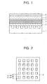
- Embodiment 1 The structure of Embodiment 1 is shown in FIG. 1.
- a diffraction grating shown in FIG. 2 was made on a glass substrate of 50mmx50mm (NA45 by HOYA, 1.1mm thick).
- an i-ray resist (THMR-iP1700 by TOKYO OHKA KOGYO CO.) was formed in a thickness of 2 ⁇ m on the glass substrate 1 by a spin coating method, and a pattern was formed with a width of 0.1 ⁇ m and a space of 0.1 ⁇ m using an i-ray stepper.
- the substrate 1 having the pattern formed therein was immersed in hydrofluoric acid solution and a groove having a depth of 100nm was formed, and thereafter the remaining resist was eliminated by a dedicated stripper liquid to thus obtain a diffraction grating 2.
- a Si 3 N 4 film was formed with a thickness of 300nm by a sputtering method using silicon nitride (Si 3 N 4 ) as a target.
- a silicon oxide (SiO 2 ) layer as an intermediate layer 3 was formed in a thickness of 50nm on the Si 3 N 4 film by the sputtering method, and then an anode 4, an organic EL layer 5, and a cathode 6 was stacked in this order on the intermediate layer 3 to make the organic EL device.
- SiO 2 silicon oxide
- a method for forming the organic EL layer 5 (a layer in which an anode 4, a hole injecting layer 8, an emitting layer 9, and a cathode 6 have been stacked in this order, as shown in FIG. 3) is as follows.
- An indium tin oxide alloy (ITO) was formed as the anode 4 on the substrate 1 by a sputtering method.
- the film thickness of the ITO presented herein was 100nm and the sheet resistance was 20 ⁇ / ⁇ .
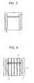
- the formed ITO was patterned using a metal mask to be a stripe of 2mm ⁇ 50mm. Further, five stripes of 2mm ⁇ 50mm were made on the substrate 1 as shown in an ITO pattern portion 11 of FIG. 4.
- a vacuum deposition apparatus used to form this organic EL layer 5 comprises a molybdenum boat filled with an evaporating material, the boat being positioned at a distance of 250mm below the substrate, placed at a upper portion of a vacuum chamber, and at an incident angle to the substrate of 38°. The substrate was rotated at 30 revolutions per minute.
- the deposition was initiated at a point of time when pressure reaches 5 ⁇ 10 -7 Torr, and a deposition rate was controlled by a crystal oscillator type film thickness control device longitudinally mounted on the substrate. Further, the deposition rate was set to 0.15nm/s.
- N,N'-diphenyl-N-N-bis(1-naphthyl)-1,1'-biphenyl)-4,4'-diamine (hereinafter, referred to as ⁇ -NMP) of 50nm as the hole injecting layer, tris(8-quinolinol)aluminum (hereinafter, referred to as ALQ) of 70nm as the light-emitting material, and magnesium-silver alloy of 150nm as the cathode were sequentially formed at a deposition rate ratio of 10:1 by co-deposition, to fabricate an organic EL device. Further, a pattern (cathode pattern 12) shown in FIG. 5 was formed using a metal mask. As a result, in the organic EL device of this embodiment, five organic EL portions 13 each having a size of 2mm ⁇ 2mm were formed on the substrate 1 in the pattern shape of the cathode 4 and the anode 6, as shown in FIG. 6.
- Embodiment 2 is the same as Embodiment 1 except that, in the structure and fabricating process, only the pitch of the diffraction grating 2 was changed to a width of 0.05 ⁇ m, a space of 0.05 ⁇ m, and a depth of 100nm.
- Embodiment 3 is the same as Embodiment 1 except that, in the structure and fabricating process, a glass substrate (NA45 by HOYA, 1.1 mm thick) of 50mm ⁇ 50mm was immersed in standard hydrofluoric acid liquid and the substrate surface was made to be coarse to form a scattering portion.
- a glass substrate NA45 by HOYA, 1.1 mm thick
- this scattering portion was buried, the intermediate layer 3 was formed, and the organic EL layer 5 was formed in the same condition as in Embodiment 1 to fabricate the organic EL device.
- Embodiment 4 is the same as Embodiment 1 except that, in the structure and fabricating process, the surface of a glass substrate (NA45 by HOYA, 1.1 mm thick) of 50mm ⁇ 50mm was rubbed with sandpaper #300, making the substrate surface to be coarse. As a result, a scattering portion was obtained.
- this scattering portion was buried, the intermediate layer 3 was formed, and the organic EL layer 5 was formed in the same condition as in Embodiment 1 to fabricate the organic EL device.
- the structure of the organic EL device of Embodiment 5 is shown in FIG. 7.
- a diffraction grating was made in the same condition as in Embodiment 1 and was buried.
- the Si 3 N 4 film was subject to a planarization process. This planarization process was made by a mechanical polishing method.
- the Si 3 N 4 film was cut out to have the residue of the film within 10nm from the diffraction grating 2 of the Si 3 N 4 film.
- a SiO 2 film as the intermediate layer 3 was formed on the Si 3 N 4 film to be a thickness of 50nm in the same condition as in Embodiment 1, and the anode 4, the organic layer 5, and the cathode 6 were formed in this order on the SiO 2 film, as shown in FIG. 7 to fabricate the organic EL device.
- the organic layer 5 is a layer obtained by stacking the hole injecting layer 8, the emitting layer 9, and the cathode 6 in this order on the anode 4.
- Embodiment 6 is the same as Embodiment 5 except that, in the structure and fabricating process, the film thickness of the SiO 2 film as the intermediate layer 3 was changed to 20nm.
- Embodiment 7 is the same as Embodiment 5 except that, in the structure and fabricating process, the film thickness of the SiO 2 film as the intermediate layer 3 was changed to 200nm.
- Embodiment 8 is the same as Embodiment 5 except that, in the structure and fabricating process, a silicon nitride (Si 3 N 4 ) film is used for the material of the intermediate layer 3. Further, the film thickness of the Si 3 N 4 film was changed to 50nm.
- Si 3 N 4 silicon nitride
- Embodiment 9 is the same as Embodiment 8 except that, in the structure and fabricating process, the film thickness of the Si 3 N 4 film as the intermediate layer 3 was changed to 100nm.
- Embodiment 10 is the same as Embodiment 8 except that, in the structure and fabricating process, the film thickness of the Si 3 N 4 film as the intermediate layer 3 was changed to 300nm.
- Embodiment 11 is the same as Embodiment 5 except that, in the structure and fabricating process, a titanium oxide (TiO 2 ) film was used for the material of the intermediate layer 3. Further, the film thickness of the TiO 2 film was 50nm.
- TiO 2 titanium oxide
- Embodiment 12 is the same as Embodiment 5 except that, in the structure and fabricating process, a zirconium dioxide (ZrO 2 ) film was used for the material of the intermediate layer 3. Further, the film thickness of the ZrO 2 film was 50nm.
- ZrO 2 zirconium dioxide
- Embodiment 13 is the same as Embodiment 5 except that, in the structure and fabricating process, a tantalum pentoxide (Ta 2 O 5 ) film was used for the material of the intermediate layer 3. Further, the film thickness of the Ta 2 O 5 film was 50nm.
- a tantalum pentoxide (Ta 2 O 5 ) film was used for the material of the intermediate layer 3. Further, the film thickness of the Ta 2 O 5 film was 50nm.
- Embodiment 14 is the same as Embodiment 5 except that, in the structure and fabricating process, an indium tin oxide (ITO) film was used for the material of the intermediate layer 3. Further, the film thickness of the ITO film was 50nm.
- ITO indium tin oxide
- Embodiment 15 is the same as Embodiment 5 except that, in the structure and fabricating process, only the method of forming the intermediate layer was changed.
- the intermediate layer (SiO 2 ) was formed by the spin coating method using sol-gel coating liquid (Si-05S by High Pure Chemical Research Institute) used to form the SiO 2 film. Further, the spin coating was carried out at the revolutions of 2000 to 5000rpm, and the baking of the sol-gel coating liquid was carried out at 500°C for 4 hours. In addition, the thickness of the SiO 2 film was 50nm.
- Embodiment 16 is the same as Embodiment 11 except that, in the structure and fabricating process, only the method of forming the intermediate layer 3 was changed.
- the intermediate layer (TiO 2 ) was formed by the spin coating method using organic metal decomposing method coating liquid (Ti-05S by High Pure Chemical Research Institute) used to form the TiO 2 film. Further, the spin coating was carried out at a revolution of 2000 to 5000rpm, and the baking of the sol-gel coating liquid was carried out at 400°C for 2 hours. In addition, the film thickness of the TiO 2 was 50nm.
- Embodiment 17 is the same as Embodiment 12 except that, in the structure and fabricating process, only the method of forming the intermediate layer was changed.
- the intermediate layer (ZrO 2 ) was formed by a spin coating method using organic metal decomposing method coating liquid (Zr-05-P by High Pure Chemical Research Institute) used to form a ZrO 2 film. Further, the spin coating was carried out at revolutions of 2000 to 5000rpm, and baking the coating liquid was carried out at 400°C for 2 hour. In addition, the thickness of the ZrO 2 film was 50nm.
- Embodiment 18 is the same as Embodiment 5 except that, in the structure and fabricating process, only the planarization process for the intermediate layer 3 was changed, in which a CMP (Chemical Mechanical Polishing) process was used to flatten a groove processing film (Si 3 N 4 ).
- CMP Chemical Mechanical Polishing
- Suba400 was used for the polishing pad
- colloidal silica polishing liquid having a particle diameter of 200nm was used for the polishing slurry.
- a commercially available CMP apparatus was used for the polisher.
- Embodiment 19 is the same as Embodiment 5 except that, in the structure and fabricating process, only the planarization process for the intermediate layer 3 was changed to a reactive ion etching process (hereinafter, referred to as RIE process).
- RIE process was carried out with a tetrafluoromethane (CF 4 ) gas for the material gas, using a commercially available RIE apparatus.
- CF 4 tetrafluoromethane
- Embodiment 20 is the same as Embodiment 5 except that, in the structure and fabricating process, only the material for the groove processing film for the diffraction grating 2 was changed, an indium tin oxide (ITO) film being used as the groove processing film. Further, the ITO film was formed by the sputtering method with the film thickness being 200nm and the refractive index being 1.83.
- ITO indium tin oxide
- Embodiment 21 is the same as Embodiment 5 except that, in the structure and fabricating process, only the material of the groove processing film for the diffraction grating was changed, a titanium oxide (TiO 2 ) film being used as the burying film. Further, the TiO 2 film was formed by the sputtering method with the film thickness being 200nm and the refractive index being 2.1.
- Embodiment 22 is the same as Embodiment 5 except that, in the structure and fabricating process, only the material of the groove processing film for the diffraction grating was changed, a zirconium dioxide (ZrO 2 ) film being used as the burying film. Further, the ZrO 2 film was formed by the sputtering method with the film thickness being 200nm and the refractive index being 2.04.
- FIG. 8 is a structure view of Comparative example 1.
- the device was configured by stacking a glass substrate 31, an anode (ITO) 32, a hole injecting layer ( ⁇ -NMP) 33, an emitting layer (AIQ) 34, and a cathode (MgAg) 35 in this order.
- ITO anode
- ⁇ -NMP hole injecting layer
- AIQ emitting layer
- MgAg cathode
- ITO indium tin oxide alloy
- the hole injecting layer 33, the emitting layer 34 and the cathode 35 were each stacked in this order on the ITO layer of the anode 32. Further, the organic layers (the hole injecting layer 33 and the emitting layer 34) and the cathode 35 were formed using a resistance-heating vacuum deposition method.
- a film-forming sequence by a vacuum deposition method will be hereinafter explained in detail.
- a molybdenum boat filled with a deposition material was disposed at a distance of 250nm downwardly from this substrate and was positioned to have an incident angle to the substrate of 38°.
- the substrate was rotated at 30 revolutions per minute.
- the deposition was initiated at a time point when pressure reaches 5 ⁇ 10 -7 Torr and a deposition rate was controlled by a crystal oscillator type film thickness control device mounted longitudinally on the substrate.
- the organic EL device was fabricated at a deposition rate of 0.15nm/s, sequentially stacking N,N'-diphenyl-N-N-bis(1-naphthyl)-1,1'-biphenyl)-4,4'-diamine (hereinafter, referred to as ⁇ -NMP) of 50nm as the hole injecting layer, tris(8-quinolinol)aluminum (hereinafter, referred to as ALQ) of 70nm as the light-emitting material, and a magnesium-silver alloy of 150nm as the cathode at a deposition rate ratio 10:1 by co-deposition.
- ⁇ -NMP N,N'-diphenyl-N-N-bis(1-naphthyl)-1,1'-biphenyl)-4,4'-diamine
- ALQ tris(8-quinolinol)aluminum
- An organic EL device was fabricated by sequentially stacking an anode, a hole injecting layer, an emitting layer, and a cathode on a quartz glass (1.1mm thick). Further, processes following the anode formation process were carried out in the same condition as Comparative example 1.
- Comparative example 3 is the same as Embodiment 1 except that only the intermediate layer was eliminated from the structure and fabricating process.
- Comparative example 4 is the same as Embodiment 2 except that only the intermediate layer was eliminated from the structure and fabricating process.
- Comparative example 5 is the same as Embodiment 3 except that only the intermediate layer was excluded from the structure and fabricating process.
- Comparative example 6 is the same as Embodiment 4 except that only the intermediate layer was eliminated from the structure and fabricating process.
- Comparative example 7 is the same as Embodiment 5 except that only the intermediate layer was eliminated from the structure and fabricating process.
- Comparative example 8 is the same as Embodiment 18 except that only the intermediate layer was eliminated from the structure and fabricating process.
- Comparative example 9 is the same as Embodiment 19 except that only the intermediate layer was eliminated from the structure and fabricating process.
- Comparative example 10 is the same as Embodiment 20 except that only the intermediate layer was eliminated from the structure and fabricating process.
- Comparative example 11 is the same as Embodiment 21 except that only the intermediate layer was eliminated from the structure and fabricating process.
- Comparative example 12 is the same as Embodiment 22 except that only the intermediate layer was eliminated from the structure and fabricating process.
- the organic EL devices of Embodiments 1 to 22 and Comparative examples 1 to 12 were subject to the characteristic evaluation of Evaluations 1 to 6. Further, the substrate of the embodiments and the comparative examples has five emission portions having a size of 2mm ⁇ 2mm (at positions A, B, C, D, and E) on the substrate 1, as shown in FIG. 9.
- the luminescence state of the emission portion was observed after applying a voltage of 10V to the organic EL device. This observation was carried out by eyes and the luminescence property was determined by the following index. Further, this evaluation was carried out four emitting portions (positions A, B, C and D) on each substrate. ⁇ : all the emitting portions exhibit good luminescence over entire surfaces. ⁇ : non-luminescence is locally observed. ⁇ : an emitting portion that does not emit light is observed.
- the lifetime was measured after a direct current of 5mA/cm 2 has been applied to the organic EL device for 100 hours.
- a change rate (Ea/Eb) between the luminous efficiency (Ea) when 100 hours has elapsed after the current application and the luminous efficiency (Eb) within 2 minutes after the current application was calculated and lifetime performance was determined by the following index. Further, this lifetime was measured at the emitting portion E.
- the deviation of the luminous efficiency on the substrate surface in each of the embodiments and the comparative examples was evaluated.
- the luminous efficiency was measured at four emitting portions (positions A, B, C and D) on each substrate, and the deviation was determined using the following determination index, where a maximum value in the four emitting portions is Emax and a minimum value is Emin. Further, the evaluation of the luminous efficiency was made by measuring the luminous efficiency upon applying a voltage of 10V as in Evaluation 1.
- ⁇ : Emin/Emax is more than 0.90 ⁇ : Emin/Emax is more than 0.80 and less than 0.90 ⁇ : Emin/Emax is less than 0.80
- Three substrates as illustrated in the embodiments and three substrates as illustrated in the comparative examples were made in the same fabrication condition, and production stability (confirmation of good luminescence reproductivity) was evaluated. This evaluation was made by observing the luminescence state of the devices on the three substrates fabricated to confirm the production reproductivity by eyes, and by using the following indexes. Further, for this evaluation, four emitting portions (positions A, B, C and D) on each of the three substrates was observed, and at totally twelve emitting portions. ⁇ : all emission portions exhibit good luminescence over entire surfaces. ⁇ : non-luminescence is locally observed. ⁇ : an emitting portion that does not emit light is observed.
- the organic electroluminescent device of the present invention has a good luminescence property and high luminous efficiency.
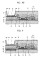
- FIG. 10 Illustrates an example of an active matrix organic light emitting display as an organic light emitting display that uses the organic light emitting element of FIG. 1.
- a buffer layer 91 is formed on a transparent substrate 90.
- the buffer layer 91 is greatly separated into a pixel region 200, which has each pixel and a transparent electrode 92 for forming the pixel, and a driving region 300 where a thin film transistor and a capacitor are formed.
- the driving region includes a gate electrode layer 94 and a first insulating film 95 burying the gate electrode layer 94, which correspond to an n or p type semiconductor layer 92 arranged in a given pattern on the buffer layer 91, present on a gate insulating layer 93 that buries the semiconductor layer 92; a thin film transistor having a drain electrode 96 and a source electrode 97 each connected to both sides of the semiconductor layer 92 via contact holes 96a and 97a formed in the first insulating film 95 and the gate insulating layer 93, and formed on a upper portion of the first insulating film 95; and a capacitor 110 composed of a first auxiliary electrode 111 connected to the source electrode 97 and formed on the first insulating layer 95, and a second auxiliary electrode 112 opposing to the first electrode and buried by the first insulting layer 95.
- a second insulating layer 98 formed on the first insulting layer 95, and a planarization film 99 with an opening 99a formed in the pixel-forming region are formed.
- a first electrode layer 100 is formed at the bottom of the opening in the planarization film 99 and is electrically connected to the drain electrode 96.
- the planarization film 99 has grooves 80 formed in the pixel-forming region. A diffraction grating is formed by the grooves 80.
- an SiO2 film as the intermediate layer 3 is formed on the planarization having the grooves in the pixel-forming region.
- An organic layer 70 is stacked on the first electrode layer 100.
- a second electrode layer 101 is formed on the organic layer and the planarization film 99.
- the grooves 80 of a diffraction grating is formed in a given pattern on the second insulating layer 98 between the transparent electrode 100 and the second insulating layer 98.
- the grooves 80 has the same configuration as in the above-stated embodiment.
- the position where the grooves 80 is to be formed is not limited to the embodiment and may be between layers with high refractive index.
- the grooves layer 80 may be formed on the substrate 90 between the substrate 90 and the buffer layer 91, as shown in FIGs. 11 and 12.
- the organic electroluminescent device it is possible to stably fabricate an organic electroluminescent device having a good luminescence property and high luminous efficiency by disposing at least one organic layer including an emitting layer between an anode and an cathode via an intermediate layer on a substrate having an optical element which is a diffraction grating, a scattering portion, a grating, or a polarizing filter.
Landscapes
- Physics & Mathematics (AREA)
- Optics & Photonics (AREA)
- Electroluminescent Light Sources (AREA)
- Diffracting Gratings Or Hologram Optical Elements (AREA)
Applications Claiming Priority (2)
| Application Number | Priority Date | Filing Date | Title |
|---|---|---|---|
| JP2003144769A JP4220305B2 (ja) | 2003-05-22 | 2003-05-22 | 有機エレクトロルミネセンス素子 |
| JP2003144769 | 2003-05-22 |
Publications (2)
| Publication Number | Publication Date |
|---|---|
| EP1480281A2 true EP1480281A2 (fr) | 2004-11-24 |
| EP1480281A3 EP1480281A3 (fr) | 2007-08-08 |
Family
ID=33095458
Family Applications (1)
| Application Number | Title | Priority Date | Filing Date |
|---|---|---|---|
| EP04090192A Withdrawn EP1480281A3 (fr) | 2003-05-22 | 2004-05-14 | Dispositif d'affichage électroluminescent |
Country Status (5)
| Country | Link |
|---|---|
| US (1) | US7619357B2 (fr) |
| EP (1) | EP1480281A3 (fr) |
| JP (1) | JP4220305B2 (fr) |
| KR (1) | KR100894625B1 (fr) |
| CN (1) | CN100459211C (fr) |
Cited By (6)
| Publication number | Priority date | Publication date | Assignee | Title |
|---|---|---|---|---|
| EP1670293A3 (fr) * | 2004-12-11 | 2007-10-24 | Samsung SDI Co., Ltd. | Dispositif d'affichage électroluminescent et méthode de fabrication |
| WO2007119954A1 (fr) * | 2006-04-14 | 2007-10-25 | Dongjin Semichem Co., Ltd | Procédé de préparation d'une mince couche organique de dispositifs électroluminescents organiques par dépôt électrochimique |
| CN100376716C (zh) * | 2004-12-08 | 2008-03-26 | 上海江信超硬材料有限公司 | 一种金刚石表面涂覆玻璃涂覆金刚石镀钛复合结构及制造方法 |
| EP2131411A1 (fr) * | 2008-06-05 | 2009-12-09 | Samsung Mobile Display Co., Ltd. | Dispositif d'affichage à diode électroluminescente organique |
| WO2010032651A1 (fr) | 2008-09-22 | 2010-03-25 | Fujifilm Corporation | Dispositif électroluminescent, procédé de fabrication associé, et afficheur contenant ce dispositif |
| WO2014077490A1 (fr) * | 2012-11-15 | 2014-05-22 | Samsung Electronics Co., Ltd. | Appareil d'affichage doté d'un panneau d'affichage auto-lumineux |
Families Citing this family (68)
| Publication number | Priority date | Publication date | Assignee | Title |
|---|---|---|---|---|
| KR100852110B1 (ko) * | 2004-06-26 | 2008-08-13 | 삼성에스디아이 주식회사 | 유기 전계 발광 소자 및 그 제조 방법 |
| JP4464210B2 (ja) * | 2004-06-29 | 2010-05-19 | 東北パイオニア株式会社 | 有機elパネルの形成方法 |
| JP2006100430A (ja) * | 2004-09-28 | 2006-04-13 | Toshiba Matsushita Display Technology Co Ltd | 有機el表示装置 |
| JP2006100140A (ja) * | 2004-09-29 | 2006-04-13 | Toshiba Matsushita Display Technology Co Ltd | 有機el表示装置の製造方法 |
| JP4511440B2 (ja) * | 2004-10-05 | 2010-07-28 | 三星モバイルディスプレイ株式會社 | 有機発光素子及び有機発光素子の製造方法 |
| KR100730121B1 (ko) * | 2004-11-29 | 2007-06-19 | 삼성에스디아이 주식회사 | 유기 전계 발광 소자 및 그 제조 방법 |
| KR100683761B1 (ko) * | 2005-02-19 | 2007-02-15 | 삼성에스디아이 주식회사 | 전계발광 디스플레이 장치 |
| US7432649B2 (en) * | 2005-02-22 | 2008-10-07 | Corning, Incorporated | Coupled waveguides for light extraction |
| US10690847B2 (en) * | 2005-06-15 | 2020-06-23 | Braggone Oy | Method of making a photonic crystal device and photonic crystal device |
| KR100708863B1 (ko) * | 2005-12-09 | 2007-04-17 | 삼성에스디아이 주식회사 | 유기 발광 표시 장치 |
| KR100749420B1 (ko) * | 2005-12-15 | 2007-08-14 | 삼성에스디아이 주식회사 | 유기 발광 표시 장치 |
| KR100728790B1 (ko) * | 2005-12-15 | 2007-06-19 | 삼성에스디아이 주식회사 | 유기 발광 표시 장치 및 그 제조 방법 |
| KR100792139B1 (ko) * | 2006-02-06 | 2008-01-04 | 주식회사 엘지화학 | 전자주입층으로서 무기절연층을 이용한 유기발광소자 및이의 제조 방법 |
| KR100932933B1 (ko) * | 2007-07-27 | 2009-12-21 | 삼성모바일디스플레이주식회사 | 편광자 및 그를 포함하는 유기 발광 표시 장치 |
| JP5428124B2 (ja) * | 2006-09-27 | 2014-02-26 | 凸版印刷株式会社 | 有機el表示体 |
| KR101367131B1 (ko) * | 2006-11-02 | 2014-02-26 | 한양대학교 산학협력단 | 유기 발광 표시 장치 및 그 제조 방법 |
| US7868542B2 (en) | 2007-02-09 | 2011-01-11 | Canon Kabushiki Kaisha | Light-emitting apparatus having periodic structure and sandwiched optical waveguide |
| US20100118522A1 (en) * | 2007-05-02 | 2010-05-13 | Koninklijke Philips Electronics N.V. | Light emitting device using oled panels in folded or deployed configuration |
| JP5057076B2 (ja) * | 2008-03-03 | 2012-10-24 | 大日本印刷株式会社 | 発光素子からの光取出し構造 |
| JP2009272194A (ja) | 2008-05-09 | 2009-11-19 | Canon Inc | 発光装置 |
| JP5167974B2 (ja) * | 2008-06-16 | 2013-03-21 | 豊田合成株式会社 | Iii族窒化物系化合物半導体発光素子及びその製造方法 |
| US8928597B2 (en) | 2008-07-11 | 2015-01-06 | Samsung Display Co., Ltd. | Organic light emitting display device |
| US8629842B2 (en) * | 2008-07-11 | 2014-01-14 | Samsung Display Co., Ltd. | Organic light emitting display device |
| US9342176B2 (en) * | 2008-07-21 | 2016-05-17 | Samsung Display Co., Ltd. | Organic light emitting display device |
| JP2010027429A (ja) * | 2008-07-22 | 2010-02-04 | Fujifilm Corp | 有機電界発光パネル及びその製造方法 |
| KR100959107B1 (ko) * | 2008-08-28 | 2010-05-25 | 삼성모바일디스플레이주식회사 | 유기 발광 표시 장치 |
| KR101058106B1 (ko) * | 2009-08-06 | 2011-08-24 | 삼성모바일디스플레이주식회사 | 표시 장치 |
| KR101094300B1 (ko) * | 2009-10-12 | 2011-12-19 | 삼성모바일디스플레이주식회사 | 유기 발광 조명 장치 및 그 제조 방법 |
| KR101318374B1 (ko) * | 2009-12-03 | 2013-10-16 | 한국전자통신연구원 | 유기 전계 발광소자 및 그 제조 방법 |
| JP5595033B2 (ja) | 2009-12-25 | 2014-09-24 | キヤノン株式会社 | 表示装置 |
| WO2011081057A1 (fr) * | 2009-12-28 | 2011-07-07 | 昭和電工株式会社 | Elément électroluminescent, procédé de fabrication d'élément électroluminescent, écran et dispositif d'éclairage |
| JP5258817B2 (ja) * | 2010-03-02 | 2013-08-07 | 株式会社東芝 | 照明装置及びその製造方法 |
| US8835962B2 (en) * | 2010-05-13 | 2014-09-16 | Sri International | Cavity electroluminescent devices with integrated microlenses |
| JP2012038542A (ja) * | 2010-08-06 | 2012-02-23 | Canon Inc | 発光素子 |
| JP5998124B2 (ja) * | 2011-03-31 | 2016-09-28 | 旭硝子株式会社 | 有機led素子、透光性基板、および透光性基板の製造方法 |
| DE102011017728A1 (de) * | 2011-04-28 | 2012-10-31 | Ledon Oled Lighting Gmbh & Co. Kg | Lichtabgebendes Element mit einer OLED oder QLED |
| KR101249029B1 (ko) * | 2011-06-07 | 2013-04-01 | 주성엔지니어링(주) | 유기 발광 장치 및 그 제조 방법 |
| CN103636290A (zh) * | 2011-06-24 | 2014-03-12 | 昭和电工株式会社 | 有机发光元件和有机发光元件的制造方法 |
| EP2541637B1 (fr) * | 2011-06-30 | 2022-01-12 | Fraunhofer-Gesellschaft zur Förderung der angewandten Forschung e.V. | Dispositif d'émission de lumière électroluminescente doté d'une structure de grille optique et son procédé de fabrication |
| KR20130108027A (ko) * | 2012-03-23 | 2013-10-02 | 주식회사 엘지화학 | 유기전자소자용 기판의 제조방법 |
| KR102036326B1 (ko) * | 2012-11-21 | 2019-10-25 | 삼성디스플레이 주식회사 | 유기 발광 표시 장치 및 그 제조 방법 |
| WO2014103891A1 (fr) * | 2012-12-28 | 2014-07-03 | 昭和電工株式会社 | Élément électroluminescent organique et dispositif d'affichage d'image et dispositif d'éclairage le comprenant |
| WO2014129444A1 (fr) * | 2013-02-20 | 2014-08-28 | 株式会社フォトニックラティス | Élément électroluminescent à rendement élevé d'extraction de l'émission lumineuse interne ainsi que substrat pour élément électroluminescent |
| KR20140119266A (ko) | 2013-03-28 | 2014-10-10 | 삼성디스플레이 주식회사 | 유기발광 표시장치 및 그 제조방법 |
| CN104078576A (zh) * | 2013-03-29 | 2014-10-01 | 海洋王照明科技股份有限公司 | 白光有机电致发光器件及其制备方法 |
| WO2015129222A1 (fr) * | 2014-02-28 | 2015-09-03 | パナソニックIpマネジメント株式会社 | Élément et dispositif électroluminescents |
| JP2016034017A (ja) | 2014-02-28 | 2016-03-10 | パナソニックIpマネジメント株式会社 | 発光装置 |
| EP3113237B1 (fr) | 2014-02-28 | 2019-04-24 | Panasonic Intellectual Property Management Co., Ltd. | Dispositif électroluminescent |
| US10739882B2 (en) | 2014-08-06 | 2020-08-11 | Apple Inc. | Electronic device display with array of discrete light-emitting diodes |
| US10031276B2 (en) | 2015-03-13 | 2018-07-24 | Panasonic Intellectual Property Management Co., Ltd. | Display apparatus including photoluminescent layer |
| US10182702B2 (en) | 2015-03-13 | 2019-01-22 | Panasonic Intellectual Property Management Co., Ltd. | Light-emitting apparatus including photoluminescent layer |
| JP6569856B2 (ja) | 2015-03-13 | 2019-09-04 | パナソニックIpマネジメント株式会社 | 発光装置および内視鏡 |
| JP2016171228A (ja) | 2015-03-13 | 2016-09-23 | パナソニックIpマネジメント株式会社 | 発光素子、発光装置および検知装置 |
| KR20160118403A (ko) * | 2015-04-01 | 2016-10-12 | 삼성디스플레이 주식회사 | 미러 기판, 이의 제조 방법 및 이를 포함하는 표시 장치 |
| JP2017003697A (ja) | 2015-06-08 | 2017-01-05 | パナソニックIpマネジメント株式会社 | 発光素子および発光装置 |
| JP2017005054A (ja) | 2015-06-08 | 2017-01-05 | パナソニックIpマネジメント株式会社 | 発光装置 |
| JP6748905B2 (ja) | 2015-08-20 | 2020-09-02 | パナソニックIpマネジメント株式会社 | 発光装置 |
| JP2017040818A (ja) | 2015-08-20 | 2017-02-23 | パナソニックIpマネジメント株式会社 | 発光素子 |
| US10359155B2 (en) | 2015-08-20 | 2019-07-23 | Panasonic Intellectual Property Management Co., Ltd. | Light-emitting apparatus |
| CN105261710B (zh) * | 2015-11-19 | 2017-05-10 | 深圳市华星光电技术有限公司 | 显示器及其有机发光二极管器件 |
| JP6719094B2 (ja) | 2016-03-30 | 2020-07-08 | パナソニックIpマネジメント株式会社 | 発光素子 |
| CN106920894B (zh) * | 2017-04-28 | 2020-04-24 | 陕西科技大学 | 一种透明oled器件结构及其制备方法 |
| WO2019031786A1 (fr) * | 2017-08-08 | 2019-02-14 | Samsung Electronics Co., Ltd. | Élément optique, élément de polarisation et dispositif d'affichage |
| CN107731864B (zh) * | 2017-11-20 | 2020-06-12 | 开发晶照明(厦门)有限公司 | 微发光二极管显示器和制作方法 |
| WO2020237430A1 (fr) * | 2019-05-24 | 2020-12-03 | Boe Technology Group Co., Ltd. | Écran d'affichage, son procédé de fabrication et appareil d'affichage |
| WO2021095194A1 (fr) * | 2019-11-14 | 2021-05-20 | シャープ株式会社 | Élément électroluminescent et dispositif d'affichage |
| CN110797385B (zh) * | 2019-12-03 | 2022-04-12 | 上海天马微电子有限公司 | 一种显示面板、显示装置以及制备方法 |
| CN114325907B (zh) * | 2020-09-30 | 2024-08-16 | 京东方科技集团股份有限公司 | 波浪形光栅、显示面板及波浪形光栅的制造方法 |
Citations (1)
| Publication number | Priority date | Publication date | Assignee | Title |
|---|---|---|---|---|
| JP2003007450A (ja) * | 2001-06-20 | 2003-01-10 | Matsushita Electric Ind Co Ltd | 発光素子、表示装置及び照明装置 |
Family Cites Families (25)
| Publication number | Priority date | Publication date | Assignee | Title |
|---|---|---|---|---|
| JPH0766856B2 (ja) | 1986-01-24 | 1995-07-19 | 株式会社小松製作所 | 薄膜el素子 |
| JP2670572B2 (ja) | 1987-06-18 | 1997-10-29 | 株式会社小松製作所 | 薄膜el素子 |
| JPH01220394A (ja) | 1988-02-29 | 1989-09-04 | Hitachi Ltd | 高輝度el素子 |
| JP2931211B2 (ja) * | 1994-09-13 | 1999-08-09 | 出光興産株式会社 | 有機el装置 |
| DE19646119A1 (de) | 1996-11-08 | 1998-05-14 | Hoechst Ag | Elektrolumineszenzvorrichtung |
| JPH118070A (ja) * | 1997-06-17 | 1999-01-12 | Casio Comput Co Ltd | 表示装置 |
| JP2991183B2 (ja) | 1998-03-27 | 1999-12-20 | 日本電気株式会社 | 有機エレクトロルミネッセンス素子 |
| JPH11329742A (ja) * | 1998-05-18 | 1999-11-30 | Idemitsu Kosan Co Ltd | 有機エレクトロルミネッセンス素子および発光装置 |
| EP1074054A2 (fr) | 1998-12-17 | 2001-02-07 | Seiko Epson Corporation | Dispositif electroluminescent |
| JP2000284726A (ja) | 1999-03-31 | 2000-10-13 | Seiko Epson Corp | 表示装置 |
| JP2001060495A (ja) | 1999-08-23 | 2001-03-06 | Tdk Corp | 有機el素子 |
| JP2001068792A (ja) | 1999-08-27 | 2001-03-16 | Canare Electric Co Ltd | 量子波干渉層を有した半導体発光素子 |
| MY141175A (en) | 2000-09-08 | 2010-03-31 | Semiconductor Energy Lab | Light emitting device, method of manufacturing the same, and thin film forming apparatus |
| JP2002131495A (ja) | 2000-10-23 | 2002-05-09 | Konica Corp | 放射線画像変換パネル |
| TW527848B (en) * | 2000-10-25 | 2003-04-11 | Matsushita Electric Industrial Co Ltd | Light-emitting element and display device and lighting device utilizing thereof |
| KR20030072349A (ko) * | 2000-11-02 | 2003-09-13 | 쓰리엠 이노베이티브 프로퍼티즈 컴파니 | 방사 디스플레이의 휘도 증대 |
| JP2002260845A (ja) * | 2001-03-02 | 2002-09-13 | Matsushita Electric Ind Co Ltd | 有機エレクトロルミネッセンス発光素子、それを用いた表示装置または発光源 |
| JP2003086353A (ja) * | 2001-09-11 | 2003-03-20 | Nissan Chem Ind Ltd | 有機el素子用透明性基板および有機el素子 |
| CN1554212A (zh) * | 2001-09-13 | 2004-12-08 | �ղ���ѧ��ҵ��ʽ���� | 有机电致发光元件用透明基板及有机电致发光元件 |
| KR100437886B1 (ko) * | 2001-09-25 | 2004-06-30 | 한국과학기술원 | 고발광효율 광결정 유기발광소자 |
| JP2003115377A (ja) * | 2001-10-03 | 2003-04-18 | Nec Corp | 発光素子、その製造方法およびこれを用いた表示装置 |
| JP2003282260A (ja) * | 2002-03-26 | 2003-10-03 | Dainippon Printing Co Ltd | エレクトロルミネッセンス表示装置 |
| JP4136799B2 (ja) * | 2002-07-24 | 2008-08-20 | 富士フイルム株式会社 | El表示素子の形成方法 |
| WO2004084323A1 (fr) * | 2003-03-19 | 2004-09-30 | Osram Opto Semiconductors Gmbh | Diode electroluminescente organique a efficacite lumineuse renforcee |
| US6911674B2 (en) * | 2003-04-16 | 2005-06-28 | Zeolux Corporation | Feedback and coupling structures and methods |
-
2003
- 2003-05-22 JP JP2003144769A patent/JP4220305B2/ja not_active Expired - Lifetime
-
2004
- 2004-05-14 EP EP04090192A patent/EP1480281A3/fr not_active Withdrawn
- 2004-05-19 KR KR1020040035753A patent/KR100894625B1/ko not_active Expired - Lifetime
- 2004-05-24 US US10/851,251 patent/US7619357B2/en not_active Expired - Lifetime
- 2004-05-24 CN CNB2004100474983A patent/CN100459211C/zh not_active Expired - Lifetime
Patent Citations (1)
| Publication number | Priority date | Publication date | Assignee | Title |
|---|---|---|---|---|
| JP2003007450A (ja) * | 2001-06-20 | 2003-01-10 | Matsushita Electric Ind Co Ltd | 発光素子、表示装置及び照明装置 |
Cited By (10)
| Publication number | Priority date | Publication date | Assignee | Title |
|---|---|---|---|---|
| CN100376716C (zh) * | 2004-12-08 | 2008-03-26 | 上海江信超硬材料有限公司 | 一种金刚石表面涂覆玻璃涂覆金刚石镀钛复合结构及制造方法 |
| EP1670293A3 (fr) * | 2004-12-11 | 2007-10-24 | Samsung SDI Co., Ltd. | Dispositif d'affichage électroluminescent et méthode de fabrication |
| US7579775B2 (en) | 2004-12-11 | 2009-08-25 | Samsung Mobile Display Co., Ltd. | Electroluminescence display device with improved external light coupling efficiency and method of manufacturing the same |
| WO2007119954A1 (fr) * | 2006-04-14 | 2007-10-25 | Dongjin Semichem Co., Ltd | Procédé de préparation d'une mince couche organique de dispositifs électroluminescents organiques par dépôt électrochimique |
| EP2131411A1 (fr) * | 2008-06-05 | 2009-12-09 | Samsung Mobile Display Co., Ltd. | Dispositif d'affichage à diode électroluminescente organique |
| US8154197B2 (en) | 2008-06-05 | 2012-04-10 | Samsung Mobile Display Co., Ltd. | Organic light emitting diode display device having refraction layers that improve light extraction efficiency and color reproducibility |
| WO2010032651A1 (fr) | 2008-09-22 | 2010-03-25 | Fujifilm Corporation | Dispositif électroluminescent, procédé de fabrication associé, et afficheur contenant ce dispositif |
| EP2356880A4 (fr) * | 2008-09-22 | 2012-09-05 | Fujifilm Corp | Dispositif électroluminescent, procédé de fabrication associé, et afficheur contenant ce dispositif |
| WO2014077490A1 (fr) * | 2012-11-15 | 2014-05-22 | Samsung Electronics Co., Ltd. | Appareil d'affichage doté d'un panneau d'affichage auto-lumineux |
| US9401464B2 (en) | 2012-11-15 | 2016-07-26 | Samsung Electronics Co., Ltd. | Display apparatus with self-luminous display panel |
Also Published As
| Publication number | Publication date |
|---|---|
| KR20040101004A (ko) | 2004-12-02 |
| EP1480281A3 (fr) | 2007-08-08 |
| JP2004349111A (ja) | 2004-12-09 |
| CN100459211C (zh) | 2009-02-04 |
| JP4220305B2 (ja) | 2009-02-04 |
| KR100894625B1 (ko) | 2009-04-24 |
| CN1575075A (zh) | 2005-02-02 |
| US7619357B2 (en) | 2009-11-17 |
| US20050077820A1 (en) | 2005-04-14 |
Similar Documents
| Publication | Publication Date | Title |
|---|---|---|
| US7619357B2 (en) | Electroluminescent display device | |
| US6476550B1 (en) | Organic Electroluminescent device with a defraction grading and luminescent layer | |
| US7345419B2 (en) | Substrate for optical element, organic electroluminescence element and organic electroluminescence display device | |
| US6998775B2 (en) | Layered, light-emitting element | |
| US7224114B2 (en) | Display device and display unit using the same | |
| US7638797B2 (en) | Substrate of emitting device and emitting device using the same | |
| US6280861B1 (en) | Organic EL device | |
| US6396208B1 (en) | Organic electroluminescent device and its manufacturing process | |
| EP2254390B1 (fr) | Element luminescent organique | |
| JP2003036969A (ja) | 発光素子、及びそれを用いた表示装置と照明装置 | |
| JP2010198921A (ja) | 透明導電膜積層体を用いた有機el素子、並びに、これらの製造方法 | |
| US7129965B2 (en) | Exposure device and image forming device | |
| JP4104339B2 (ja) | 発光素子及びその製造方法、並びに表示装置 | |
| JP2006269235A (ja) | 有機エレクトロルミネッセンス素子の製造方法及び有機エレクトロルミネッセンス素子 | |
| JP2004335301A (ja) | 有機エレクトロルミネセンス素子用基板の製造方法 | |
| JP4303031B2 (ja) | 有機エレクトロルミネセンス素子用基板の製造方法 | |
| JP4382388B2 (ja) | 有機エレクトロルミネセンス素子用基板、ならびにこれを用いた有機エレクトロルミネセンス素子 |
Legal Events
| Date | Code | Title | Description |
|---|---|---|---|
| PUAI | Public reference made under article 153(3) epc to a published international application that has entered the european phase |
Free format text: ORIGINAL CODE: 0009012 |
|
| AK | Designated contracting states |
Kind code of ref document: A2 Designated state(s): AT BE BG CH CY CZ DE DK EE ES FI FR GB GR HU IE IT LI LU MC NL PL PT RO SE SI SK TR |
|
| AX | Request for extension of the european patent |
Extension state: AL HR LT LV MK |
|
| PUAL | Search report despatched |
Free format text: ORIGINAL CODE: 0009013 |
|
| AK | Designated contracting states |
Kind code of ref document: A3 Designated state(s): AT BE BG CH CY CZ DE DK EE ES FI FR GB GR HU IE IT LI LU MC NL PL PT RO SE SI SK TR |
|
| AX | Request for extension of the european patent |
Extension state: AL HR LT LV MK |
|
| 17P | Request for examination filed |
Effective date: 20080108 |
|
| 17Q | First examination report despatched |
Effective date: 20080305 |
|
| AKX | Designation fees paid |
Designated state(s): DE FR GB |
|
| RAP1 | Party data changed (applicant data changed or rights of an application transferred) |
Owner name: SAMSUNG MOBILE DISPLAY CO., LTD. |
|
| RAP1 | Party data changed (applicant data changed or rights of an application transferred) |
Owner name: SAMSUNG DISPLAY CO., LTD. |
|
| RAP1 | Party data changed (applicant data changed or rights of an application transferred) |
Owner name: SAMSUNG DISPLAY CO., LTD. |
|
| STAA | Information on the status of an ep patent application or granted ep patent |
Free format text: STATUS: THE APPLICATION HAS BEEN WITHDRAWN |
|
| 18W | Application withdrawn |
Effective date: 20170803 |