EP1480441A1 - Méthode et dispositif d'imagerie multipiste utilisant des faisceaux monomodes et des optiques limitées par diffraction - Google Patents
Méthode et dispositif d'imagerie multipiste utilisant des faisceaux monomodes et des optiques limitées par diffraction Download PDFInfo
- Publication number
- EP1480441A1 EP1480441A1 EP04076432A EP04076432A EP1480441A1 EP 1480441 A1 EP1480441 A1 EP 1480441A1 EP 04076432 A EP04076432 A EP 04076432A EP 04076432 A EP04076432 A EP 04076432A EP 1480441 A1 EP1480441 A1 EP 1480441A1
- Authority
- EP
- European Patent Office
- Prior art keywords
- slm
- beams
- recited
- recording medium
- imaging
- Prior art date
- Legal status (The legal status is an assumption and is not a legal conclusion. Google has not performed a legal analysis and makes no representation as to the accuracy of the status listed.)
- Granted
Links
Images


Classifications
-
- B—PERFORMING OPERATIONS; TRANSPORTING
- B41—PRINTING; LINING MACHINES; TYPEWRITERS; STAMPS
- B41J—TYPEWRITERS; SELECTIVE PRINTING MECHANISMS, i.e. MECHANISMS PRINTING OTHERWISE THAN FROM A FORME; CORRECTION OF TYPOGRAPHICAL ERRORS
- B41J2/00—Typewriters or selective printing mechanisms characterised by the printing or marking process for which they are designed
- B41J2/435—Typewriters or selective printing mechanisms characterised by the printing or marking process for which they are designed characterised by selective application of radiation to a printing material or impression-transfer material
- B41J2/447—Typewriters or selective printing mechanisms characterised by the printing or marking process for which they are designed characterised by selective application of radiation to a printing material or impression-transfer material using arrays of radiation sources
- B41J2/45—Typewriters or selective printing mechanisms characterised by the printing or marking process for which they are designed characterised by selective application of radiation to a printing material or impression-transfer material using arrays of radiation sources using light-emitting diode [LED] or laser arrays
- B41J2/451—Special optical means therefor, e.g. lenses, mirrors, focusing means
-
- B—PERFORMING OPERATIONS; TRANSPORTING
- B41—PRINTING; LINING MACHINES; TYPEWRITERS; STAMPS
- B41J—TYPEWRITERS; SELECTIVE PRINTING MECHANISMS, i.e. MECHANISMS PRINTING OTHERWISE THAN FROM A FORME; CORRECTION OF TYPOGRAPHICAL ERRORS
- B41J2/00—Typewriters or selective printing mechanisms characterised by the printing or marking process for which they are designed
- B41J2/435—Typewriters or selective printing mechanisms characterised by the printing or marking process for which they are designed characterised by selective application of radiation to a printing material or impression-transfer material
- B41J2/465—Typewriters or selective printing mechanisms characterised by the printing or marking process for which they are designed characterised by selective application of radiation to a printing material or impression-transfer material using masks, e.g. light-switching masks
-
- B—PERFORMING OPERATIONS; TRANSPORTING
- B41—PRINTING; LINING MACHINES; TYPEWRITERS; STAMPS
- B41J—TYPEWRITERS; SELECTIVE PRINTING MECHANISMS, i.e. MECHANISMS PRINTING OTHERWISE THAN FROM A FORME; CORRECTION OF TYPOGRAPHICAL ERRORS
- B41J2/00—Typewriters or selective printing mechanisms characterised by the printing or marking process for which they are designed
- B41J2/435—Typewriters or selective printing mechanisms characterised by the printing or marking process for which they are designed characterised by selective application of radiation to a printing material or impression-transfer material
- B41J2/47—Typewriters or selective printing mechanisms characterised by the printing or marking process for which they are designed characterised by selective application of radiation to a printing material or impression-transfer material using the combination of scanning and modulation of light
- B41J2/471—Typewriters or selective printing mechanisms characterised by the printing or marking process for which they are designed characterised by selective application of radiation to a printing material or impression-transfer material using the combination of scanning and modulation of light using dot sequential main scanning by means of a light deflector, e.g. a rotating polygonal mirror
- B41J2/473—Typewriters or selective printing mechanisms characterised by the printing or marking process for which they are designed characterised by selective application of radiation to a printing material or impression-transfer material using the combination of scanning and modulation of light using dot sequential main scanning by means of a light deflector, e.g. a rotating polygonal mirror using multiple light beams, wavelengths or colours
-
- G—PHYSICS
- G02—OPTICS
- G02B—OPTICAL ELEMENTS, SYSTEMS OR APPARATUS
- G02B26/00—Optical devices or arrangements for the control of light using movable or deformable optical elements
- G02B26/08—Optical devices or arrangements for the control of light using movable or deformable optical elements for controlling the direction of light
- G02B26/0816—Optical devices or arrangements for the control of light using movable or deformable optical elements for controlling the direction of light by means of one or more reflecting elements
- G02B26/0833—Optical devices or arrangements for the control of light using movable or deformable optical elements for controlling the direction of light by means of one or more reflecting elements the reflecting element being a micromechanical device, e.g. a MEMS mirror, DMD
-
- G—PHYSICS
- G02—OPTICS
- G02B—OPTICAL ELEMENTS, SYSTEMS OR APPARATUS
- G02B27/00—Optical systems or apparatus not provided for by any of the groups G02B1/00 - G02B26/00, G02B30/00
- G02B27/0025—Optical systems or apparatus not provided for by any of the groups G02B1/00 - G02B26/00, G02B30/00 for optical correction, e.g. distorsion, aberration
- G02B27/0037—Optical systems or apparatus not provided for by any of the groups G02B1/00 - G02B26/00, G02B30/00 for optical correction, e.g. distorsion, aberration with diffracting elements
-
- G—PHYSICS
- G02—OPTICS
- G02B—OPTICAL ELEMENTS, SYSTEMS OR APPARATUS
- G02B27/00—Optical systems or apparatus not provided for by any of the groups G02B1/00 - G02B26/00, G02B30/00
- G02B27/42—Diffraction optics, i.e. systems including a diffractive element being designed for providing a diffractive effect
- G02B27/4205—Diffraction optics, i.e. systems including a diffractive element being designed for providing a diffractive effect having a diffractive optical element [DOE] contributing to image formation, e.g. whereby modulation transfer function MTF or optical aberrations are relevant
- G02B27/4227—Diffraction optics, i.e. systems including a diffractive element being designed for providing a diffractive effect having a diffractive optical element [DOE] contributing to image formation, e.g. whereby modulation transfer function MTF or optical aberrations are relevant in image scanning systems
-
- H—ELECTRICITY
- H04—ELECTRIC COMMUNICATION TECHNIQUE
- H04N—PICTORIAL COMMUNICATION, e.g. TELEVISION
- H04N1/00—Scanning, transmission or reproduction of documents or the like, e.g. facsimile transmission; Details thereof
- H04N1/04—Scanning arrangements, i.e. arrangements for the displacement of active reading or reproducing elements relative to the original or reproducing medium, or vice versa
- H04N1/06—Scanning arrangements, i.e. arrangements for the displacement of active reading or reproducing elements relative to the original or reproducing medium, or vice versa using cylindrical picture-bearing surfaces, i.e. scanning a main-scanning line substantially perpendicular to the axis and lying in a curved cylindrical surface
- H04N1/0607—Scanning a concave surface, e.g. with internal drum type scanners
- H04N1/0621—Scanning a concave surface, e.g. with internal drum type scanners using a picture-bearing surface stationary in the main-scanning direction
- H04N1/0635—Scanning a concave surface, e.g. with internal drum type scanners using a picture-bearing surface stationary in the main-scanning direction using oscillating or rotating mirrors
-
- H—ELECTRICITY
- H04—ELECTRIC COMMUNICATION TECHNIQUE
- H04N—PICTORIAL COMMUNICATION, e.g. TELEVISION
- H04N1/00—Scanning, transmission or reproduction of documents or the like, e.g. facsimile transmission; Details thereof
- H04N1/04—Scanning arrangements, i.e. arrangements for the displacement of active reading or reproducing elements relative to the original or reproducing medium, or vice versa
- H04N1/06—Scanning arrangements, i.e. arrangements for the displacement of active reading or reproducing elements relative to the original or reproducing medium, or vice versa using cylindrical picture-bearing surfaces, i.e. scanning a main-scanning line substantially perpendicular to the axis and lying in a curved cylindrical surface
- H04N1/0664—Scanning arrangements, i.e. arrangements for the displacement of active reading or reproducing elements relative to the original or reproducing medium, or vice versa using cylindrical picture-bearing surfaces, i.e. scanning a main-scanning line substantially perpendicular to the axis and lying in a curved cylindrical surface with sub-scanning by translational movement of the picture-bearing surface
-
- H—ELECTRICITY
- H04—ELECTRIC COMMUNICATION TECHNIQUE
- H04N—PICTORIAL COMMUNICATION, e.g. TELEVISION
- H04N1/00—Scanning, transmission or reproduction of documents or the like, e.g. facsimile transmission; Details thereof
- H04N1/04—Scanning arrangements, i.e. arrangements for the displacement of active reading or reproducing elements relative to the original or reproducing medium, or vice versa
- H04N1/19—Scanning arrangements, i.e. arrangements for the displacement of active reading or reproducing elements relative to the original or reproducing medium, or vice versa using multi-element arrays
- H04N1/191—Scanning arrangements, i.e. arrangements for the displacement of active reading or reproducing elements relative to the original or reproducing medium, or vice versa using multi-element arrays the array comprising a one-dimensional [1D] array
- H04N1/1911—Simultaneously or substantially simultaneously scanning picture elements on more than one main scanning line, e.g. scanning in swaths
-
- H—ELECTRICITY
- H04—ELECTRIC COMMUNICATION TECHNIQUE
- H04N—PICTORIAL COMMUNICATION, e.g. TELEVISION
- H04N1/00—Scanning, transmission or reproduction of documents or the like, e.g. facsimile transmission; Details thereof
- H04N1/04—Scanning arrangements, i.e. arrangements for the displacement of active reading or reproducing elements relative to the original or reproducing medium, or vice versa
- H04N1/06—Scanning arrangements, i.e. arrangements for the displacement of active reading or reproducing elements relative to the original or reproducing medium, or vice versa using cylindrical picture-bearing surfaces, i.e. scanning a main-scanning line substantially perpendicular to the axis and lying in a curved cylindrical surface
- H04N1/0607—Scanning a concave surface, e.g. with internal drum type scanners
-
- H—ELECTRICITY
- H04—ELECTRIC COMMUNICATION TECHNIQUE
- H04N—PICTORIAL COMMUNICATION, e.g. TELEVISION
- H04N1/00—Scanning, transmission or reproduction of documents or the like, e.g. facsimile transmission; Details thereof
- H04N1/04—Scanning arrangements, i.e. arrangements for the displacement of active reading or reproducing elements relative to the original or reproducing medium, or vice versa
- H04N1/113—Scanning arrangements, i.e. arrangements for the displacement of active reading or reproducing elements relative to the original or reproducing medium, or vice versa using oscillating or rotating mirrors
- H04N1/1135—Scanning arrangements, i.e. arrangements for the displacement of active reading or reproducing elements relative to the original or reproducing medium, or vice versa using oscillating or rotating mirrors for the main-scan only
Definitions
- This invention is related to imaging multiple tracks simultaneously using a beam multiplier to form a set of single-mode beams and a spatial light modulator (SLM) to modulate the single-mode beams to form the tracks, such that diffraction-limited optics can be used to focus the beams.
- SLM spatial light modulator
- MEMS Micro Electromechanical Systems
- a relatively large number of modulated beams enables lowering the rotational speed of a polygon in the case of a stationary internal drum imaging system using a polygon, and lowering the rotational speed of a drum in the case of an external drum imaging system.
- Multichannel imaging is also useful in other fields of application.
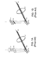
- FIG. 1A shows in simplified form one example of a prior art imaging system that uses a line-shaped laser diode source 101 and a lens 103 to illuminate a multichannel spatial light modulator (SLM) 105.
- the SLM 105 separates the beam illuminating the SLM 105 into a plurality of individually modulated beams 106 that are imaged using an optical system ⁇ shown in simple form as lens 107 ⁇ onto a light sensitive surface on an image plane 109 that, for example, might be the inside surface of an internal drum imager, or the outside surface of an external drum imager.
- the plurality of signals that modulate the plurality of beams, or the mechanism used to provide relative motion between the beams on the imaging plane, and the light sensitive surface on which an image is being formed.
- the relative motion may be provided by moving the beam, e.g., using a rotating polygon in an internal drum scanner, or by moving the radiation-sensitive surface of the recording medium, e.g., rotating the drum of an external drum scanner.
- FIG. 1B shows in simplified form another example of a prior art imaging system, this one using an array of laser diode sources 111 and an array of lenslets 113 to illuminate an SLM 115, replacing the single line-shaped source 101 and lens 103 of FIG. 1A.
- the remainder of the system is similar to that of FIG. 1A. That is, SLM 115 separates the beams illuminating the SLM 115 into a plurality of individually modulated beams 116 that are imaged using an optical system 117 onto a light sensitive surface on an image plane 119.
- FIG. 1B also does not show the mechanism for providing relative motion between the modulated beams hitting the light sensitive material and the light sensitive material itself.
- the SLM is a two-dimensional array of light modulators.
- One of the drawbacks of the prior art using either an array of laser diodes or a large area or line-shaped laser diode source is that the beam is of relatively poor quality.
- line-shaped and large-area sources also known as multimode sources
- the beam quality given by the parameter M 2 , ranges from 1 for a diffraction-limited TEM00 Gaussian laser beam, to several hundred for a distorted, poor quality beam.
- the optics of a prior art imaging system needs to be carefully designed with tight tolerances and be of high quality. This increasing the system costs and decreasing the reliability.
- an autofocus system is used to overcome the shallow depth of focus of the optical system, e.g., lens 107 or 117, used in prior art systems.
- SLMs are desirable to provide for multichannel imaging, yet it is also desirable to maintain diffraction-limited beam properties. This leads to increased depth of focus and enhanced imaging quality in comparison to conventional imaging optics involving SLMs.
- the imaging apparatus includes a laser beam source to generate single-mode laser beam of energy, a multichannel spatial light modulator (SLM) accepting a plurality of modulating signals, and a beam multiplier between the radiation source and the SLM.
- the beam multiplier accepts the beam generated by the source and generates from that beam a plurality of beams directed onto the SLM.
- the beams from the beam multiplier illuminate the active region of the SLM such that the SLM generates a plurality of modulated beams modulated according to the modulating signals.
- the system further includes an optical subsystem located between the SLM and an imaging plane that includes at least one optical element to focus the modulated beams onto an imaging plane.
- a recording medium sensitive to imaging radiation from the source is placed at the imaging plane.
- the recording medium is capable of being permanently marked in response to incidence of such imaging radiation.
- the beams generated by the SLM are each substantially a single-mode beam such that the first optical subsystem may be designed using diffraction-limited optics.
- Described herein is a multichannel imaging system that uses an initial single-mode laser beam and generates multiple single-mode beams from the initial beam to illuminate a multichannel SLM. Illuminating the SLM by multiple single-mode beams generated modulated single-mode beams and allows diffraction-limited optics to be used to form multiple tracks on a radiation-sensitive surface of a recording medium.
- FIG. 2 shows one embodiment of an imaging system 200.
- the system of FIG. 2 is shown in a simplified form to describe the inventive aspects and not mask such aspects with unnecessary detail. Furthermore, dimensions and angle proportions are strongly exaggerated.
- the system 200 includes a radiation or laser beam source 201 to generate a single-mode laser beam of energy 203, a multichannel spatial light modulator (SLM) 215 accepting a plurality of modulating signals 217, and a beam multiplier 205 between the radiation or laser beam source 201 and the SLM 215.
- SLM spatial light modulator
- the beam multiplier 205 accepts the single-mode laser beam 203 and generates from this beam 203 a plurality of beams 209 directed onto the SLM 215 to illuminate the active region of the SLM 215 such that SLM 215 generates a plurality of modulated beams 219 each modulated according to one of the modulating signals 217.
- the system further includes an optical focusing subsystem located between the SLM 215 and an imaging plane 223.
- the focusing subsystem includes at least one optical element, shown as lens 221, to focus the modulated beams 219 onto the imaging plane 223.
- a recording medium 225 which may be sensitive to imaging radiation from the radiation or laser beam source 201, is placed at the imaging plane 223.
- the recording medium 225 is capable of being permanently marked in response to incidence of such imaging radiation.
- the modulated beams 219 generated by the SLM 215 are each substantially a single-mode beam such that the first optical subsystem may be designed using diffraction-limited optics.
- FIG. 2 Not shown in FIG. 2 is a mechanism to provide relative motion between the modulated beams 219 incident on the imaging plane 223 and the recording medium 225. With such a mechanism, the apparatus simultaneously records a plurality of data tracks on the recording medium 225.
- FIG. 5 and 6 each show a system that includes such a relative motion mechanism, one system including a rotating external drum and the second system including a rotating polygon that scans beams across an internal curved surface.
- the SLM 215 is a reflective device that includes a plurality of reflective elements distributed along a long axis.
- the SLM 215 is a MEM device with reflective elements constructed using micromachined silicon and distributed along a long axis.
- One embodiment of system 200 includes a second optical subsystem 211 between the laser beam source 201 and the SLM 215 to elongate the cross-sectional distribution of each of the beams 209 in the direction of the SLM's long axis. This is done so that more of the energy of the beams 209 is directed towards the optically active part of the SLM 215 than in the case of not so elongating the beams' cross-sections.
- the result is a set of beams 213 each having a cross-sectional distribution with a short axis and a long axis, e.g., an elliptically shaped distribution.
- Each beam's long axis is parallel to the SLM's long axis.
- the beams 213 are distributed in the direction of the SLM's long axes.
- the beam 203 generated by single-mode laser beam source 201 has a circularly symmetric Gaussian cross-sectional distribution.
- FIG. 3A shows a representation 300 of such a cross-sectional distribution.
- FIG. 3B shows the representation 310 of the cross-sectional distribution of one of the beams 213 incident on the SLM 215 after passing through the beam multiplier 205 and the second optical subsystem 211 that elongates the beam's cross-sectional distribution, The beam's cross section is approximately elliptically shaped.
- FIG. 3C shows another representation of the elliptically shaped cross-sectional distribution.
- the second optical subsystem 211 includes at least one cylindrical lens.
- the second optical subsystem includes an array of lenslets that together cause elongation of the cross-sectional distributions of the beams 209.
- the distance between the focussed beams on the imaging plane 223 may be varied by changing the angles between the beams 209 from the beam multiplier 205.
- each beam is incident on a single element, e.g., a reflective element of an SLM 215.
- the resolution of the system can only be changed in steps that correspond to one or multiples of the distance between the elements of the SLM 215.
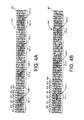
- FIG. 4A shows a set 400 of the elements 403 of the SLM 215.
- Four beams 405-1, 405-2, 4-5-3, and 405-4 are shown incident on four subsets of the elements 403, shown as subsets 407-1, 407-2, 407-3, and 407-4, respectively.
- Each of the subsets 407-1 to 4 forms a macro-cell of the SLM 215.
- Controlling each macro-cell involves controlling all the elements 403 of a particular subset 407-1 to 4 in unison. Such control of a macro-cell generates each modulated beam of the set of beams 219.
- FIG. 2 assumes that the SLM 215 includes electronics that cause each subset of elements 403 of the SLM 215 to move in unison in response to the corresponding one of modulating signals 217.
- each modulated beam has a corresponding subset 407-1 to 4 of SLM elements 403 controlled by one of the modulating signals 217.
- the distance between the beams 219 on the imaging plane 225 may be varied by varying the angles between the beams 213 out of the beam multiplier 205. As shown in FIG. 4B, so changing the distance between the beams changes the number of SLM elements 403 in each macro-cell that modulates each individual beam.
- FIG. 4B shows the same SLM elements 403 as shown in FIG. 4A, but now with beams 213 that are wider and more widely separated on the active region, such that only three complete beams, 415-1, 415-2, and 415-3 fall on the shown part of the active region. Different subsets of the elements 403 form the macro-cells, shown as 417-1, 417-2, and 417-3, for modulating beams 415-1, 415-2, and 415-3, respectively.
- the electronics between the modulating signals 217 and the drivers of the SLM elements 403 are configured such that adjusting the distance between the beams also adjusts which subsets of SLM elements 403 form macro-cells 417-1, 417-2, and 417-3. Each element 403 in each subset 407-1 to 4 is then modulated in unison by one of the modulating signals 217.
- the SLM 215 of FIG. 2 thus assumes that such driving electronics is included in the SLM 215.
- system 200 is directed to exposing light sensitive flexographic plate material to create flexographic printing plates. While such an embodiment is now described in more detail, other embodiments may be used for other applications.
- the laser beam source 201 is of a wavelength and energy to expose a flexographic plate.
- the laser beam source 201 generates single-mode beam 203 of infrared (IR) radiation.
- One version uses a fiber laser that generates a TEM00 mode CW IR beam.
- One such laser is a fiber laser made by IPG Photonics Corporation, Oxford, Massachusetts.
- One IPG laser that can be used operates at an output power of about 50W at a wavelength of 1080 nm.
- Another operates at a power of 100W.
- Yet another at a wavelength of 1600 nm.
- An alternate embodiment operates with a laser beam source that generates a quasi-CW beam.
- the beam multiplier 205 uses an acousto-optic deflector.
- deflectors are well known, and typically include a substantially transparent crystal whose index of refraction is varied periodically by causing a periodic sound wave to travel across the crystal by applying a radio-frequency (RF) signal to an included piezoelectric RF transducer.
- the periodic refraction pattern causes the crystal to act as a diffraction grating producing Bragg diffraction.
- the undiffracted laser beam is called the zero order laser beam and the primary diffracted beam is called the first order laser beam.
- the first order beam is used for imaging. Alternate embodiments may use higher order beams.
- a single beam may be directed in a particular direction. Unwanted beams are absorbed by one or more included beam dumps. Note that FIG. 2 does not show any of the beam dumps for the case of using an acousto-optic deflector for the beam multiplier 205. Those in the art would know to include, and where and how to include such beam dumps in the system 200.
- an acousto-optic deflector is fed with an RF signal that is decomposable as a sum of signals each at a distinct RF frequency. This generates a set of beams each deflected by an amount dependent on one of the RF frequencies.
- the beam multiplier 205 includes a acousto-optic deflector fed by an RF signal 207 decomposable as a sum of signals of distinct RF frequencies selected to provide the deflections appropriate for the distance between the beams on the imaging plane 223.
- the magnitudes of the signals from the beam multiplier 205 are approximately equal, but may vary depending on the efficiency vs. frequency characteristics of the device.
- the acousto-optic deflector of beam multiplier 205 is made by AA Opto-Electronique, St. Remy Les Chevreuse, France.
- the number of beams is the order of eighty, so that the RF signal 207 is decomposable to sum of eighty signals of eighty distinct frequencies selected to produce beams focussed at equidistant points on the imaging plane 223.
- the eighty frequencies are centered around 75MHz.
- the distance between the focussed beams on the imaging plane is varied by changing the RF frequencies of the RF signal 207 applied to the beam multiplier 205.
- the arrangement of which elements 403 from the macro-cells 417-1 to 3 also is changed as described above and in FIG. 4A and 4B.
- the beam multiplier 205 includes a diffractive beam sampler.
- Diffractive beam samplers are made by Gentec-EO Inc., Quebec City, Quebec, Canada, and also by Holo/Or Ltd., Kiryat Weizman, Rehovot, Israel.
- Such a diffractive beam sampler may be made as a diffractive phase grating of a Dammann type. A prescribed number of diffraction orders feature equal intensity, while the others orders are of negligible intensity.
- the SLM 215 is a one-dimensional multichannel MEM array made by Silicon Light Machines of Sunnyvale, California, part of Cypress Semiconductor Corporation of San Jose, California. Silicon Light Machines refers to its SLMs as Grating Light Valves (GLVs), and thus the term SLM will be understood to include a GLV.
- GLVs Grating Light Valves
- FIG. 5 and 6 each shows one embodiment of an imaging system that includes the elements of FIG. 2 together with a mechanism to provide relative motion between the modulated beams 219 incident on the imaging plane 223 and the recording medium 225.
- the relative motion provides for the system to simultaneously record a plurality of data tracks on the recording medium 225 when the medium is at the imaging plane 223.
- FIG. 5 shows an external drum imaging system 500, e.g., for imaging flexographic plate material that has been applied to an imaging sleeve.
- the system includes, in addition to the elements of FIG. 2, a rotatable external drum 503 on which the recording medium 507 is held using an imaging sleeve 505. Also included is a motor drive 509 for rotating the drum 503, thus providing the relative motion between the focussed beams and the recording medium 507.
- FIG. 5 is not in scale and may include other elements excluded from the description to not obscure the inventive aspects. Not shown, for example, is a mechanism to provide relative motion in a direction parallel to the axis of rotation of the drum 503.
- FIG. 5 shows a general system.
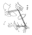
- FIG. 6 shows an internal drum imaging system 600.
- the system 600 includes, in addition to the elements of FIG. 2, an inwardly curving plate having an inwardly curving internal surface 603 on which the recording medium is placed.
- the internal surface 603 has a circumferential direction 605 and a longitudinal direction 607.
- the imaging plane 223 is along the internal surface 603.
- the apparatus includes a mechanism to provide relative motion that moves the beams along the circumferential direction 605 of the inwardly curving surface 603.
- the mechanism to provide the relative motion is multi-faced polygon 609 that causes the beams to move in the circumferential direction 605. Included is a motor drive 611 for rotating the multi-faced polygon 609, thus providing the relative motion between the focussed beams and the recording medium.
- FIG. 6 is also not in scale.
- the multi-faced polygon 609 for example, is shown exaggerated, and with only six faces. Other elements are excluded from FIG. 6 and the description to not obscure the inventive aspects. Not shown, for example, is a mechanism to provide relative motion in the longitudinal direction 607.
- the apparatuses described above each implement a method of imaging multiple tracks simultaneously.
- the method includes generating a single-mode beam of energy and directing said beam towards a beam multiplier, generating a set of single-mode beams using the beam multiplier onto which the beam of energy is directed, illuminating an SLM using the set of beams to form a set of modulated beams, and focussing the set of modulated beams onto an imaging plane at which a recording medium sensitive to imaging radiation may be placed.
- the recording medium is capable of being permanently marked in response to incidence of such imaging radiation.
- the method allows using diffraction-limited optics for the focussing.
- the invention is not limited to any one type of imaging architecture and method of imaging, and thus may be utilized in conjunction with one or a combination of other architectures.
- the invention is not limited to imaging on a drum or on a curved surface, and may be adapted to imaging a planer recording medium by including the necessary optics to form beams along a flat planar surface.
- the imaging system for example, may be used to expose printed circuit boards.
Landscapes
- Physics & Mathematics (AREA)
- Optics & Photonics (AREA)
- Engineering & Computer Science (AREA)
- Multimedia (AREA)
- Signal Processing (AREA)
- General Physics & Mathematics (AREA)
- Health & Medical Sciences (AREA)
- General Health & Medical Sciences (AREA)
- Toxicology (AREA)
- Mechanical Light Control Or Optical Switches (AREA)
- Exposure And Positioning Against Photoresist Photosensitive Materials (AREA)
Applications Claiming Priority (2)
| Application Number | Priority Date | Filing Date | Title |
|---|---|---|---|
| US442666 | 2003-05-21 | ||
| US10/442,666 US6873398B2 (en) | 2003-05-21 | 2003-05-21 | Method and apparatus for multi-track imaging using single-mode beams and diffraction-limited optics |
Publications (2)
| Publication Number | Publication Date |
|---|---|
| EP1480441A1 true EP1480441A1 (fr) | 2004-11-24 |
| EP1480441B1 EP1480441B1 (fr) | 2008-11-12 |
Family
ID=33097989
Family Applications (1)
| Application Number | Title | Priority Date | Filing Date |
|---|---|---|---|
| EP04076432A Expired - Lifetime EP1480441B1 (fr) | 2003-05-21 | 2004-05-14 | Méthode et dispositif d'imagerie multipiste utilisant des faisceaux monomodes et des optiques limitées par diffraction |
Country Status (3)
| Country | Link |
|---|---|
| US (1) | US6873398B2 (fr) |
| EP (1) | EP1480441B1 (fr) |
| DE (1) | DE602004017668D1 (fr) |
Cited By (1)
| Publication number | Priority date | Publication date | Assignee | Title |
|---|---|---|---|---|
| EP2071401A2 (fr) | 2006-04-04 | 2009-06-17 | tesa scribos GmbH | Dispositif et procédé de micro-structuration d'un support de stockage et support de stockage doté d'une zone micro-structurée |
Families Citing this family (22)
| Publication number | Priority date | Publication date | Assignee | Title |
|---|---|---|---|---|
| DE102006040843B4 (de) * | 2005-08-31 | 2015-04-16 | Heidelberger Instruments Mikrotechnik Gmbh | Vorrichtung zur optischen Aufspaltung und Modulation von elektromagnetischer Strahlung |
| US7826130B2 (en) * | 2005-08-31 | 2010-11-02 | Heidelberg Instruments Mikrotechnik Gmbh | Device for the optical splitting and modulation of electromagnetic radiation |
| US9429742B1 (en) | 2011-01-04 | 2016-08-30 | Nlight, Inc. | High power laser imaging systems |
| US10095016B2 (en) | 2011-01-04 | 2018-10-09 | Nlight, Inc. | High power laser system |
| US9409255B1 (en) | 2011-01-04 | 2016-08-09 | Nlight, Inc. | High power laser imaging systems |
| US9645502B2 (en) * | 2011-04-08 | 2017-05-09 | Asml Netherlands B.V. | Lithographic apparatus, programmable patterning device and lithographic method |
| US9720244B1 (en) * | 2011-09-30 | 2017-08-01 | Nlight, Inc. | Intensity distribution management system and method in pixel imaging |
| US9310248B2 (en) | 2013-03-14 | 2016-04-12 | Nlight, Inc. | Active monitoring of multi-laser systems |
| US9709810B2 (en) | 2014-02-05 | 2017-07-18 | Nlight, Inc. | Single-emitter line beam system |
| JP6600351B2 (ja) | 2014-08-07 | 2019-10-30 | オルボテック リミテッド | Liftプリント・システム |
| EP3207772B1 (fr) | 2014-10-19 | 2024-04-17 | Orbotech Ltd. | Impression par transfert avant induit par laser de tracés conducteurs sur un substrat semi-conducteur |
| CN107111205B (zh) | 2014-11-12 | 2020-12-15 | 奥宝科技有限公司 | 具有多个输出光束的声光偏光器 |
| EP3247816A4 (fr) | 2015-01-19 | 2018-01-24 | Orbotech Ltd. | Impression de structures métalliques tridimensionnelles avec un support sacrificiel |
| CN107849687B (zh) | 2015-07-09 | 2020-01-14 | 奥博泰克有限公司 | 对激光诱导正向转移喷射角度的控制 |
| EP3377290B1 (fr) | 2015-11-22 | 2023-08-02 | Orbotech Ltd. | Contrôle des propriétés de surface de structures tridimensionnelles imprimées |
| DE102016124408A1 (de) | 2016-12-14 | 2018-06-14 | Lilas Gmbh | Vorrichtung zur Ablenkung und/oder Modulation einer Laserstrahlung, insbesondere einer Mehrzahl von Laserstrahlen |
| US10904514B2 (en) | 2017-02-09 | 2021-01-26 | Facebook Technologies, Llc | Polarization illumination using acousto-optic structured light in 3D depth sensing |
| TW201901887A (zh) | 2017-05-24 | 2019-01-01 | 以色列商奧寶科技股份有限公司 | 於未事先圖樣化基板上電器互連電路元件 |
| US10613413B1 (en) | 2017-05-31 | 2020-04-07 | Facebook Technologies, Llc | Ultra-wide field-of-view scanning devices for depth sensing |
| US10181200B1 (en) | 2017-06-28 | 2019-01-15 | Facebook Technologies, Llc | Circularly polarized illumination and detection for depth sensing |
| CN107315176B (zh) * | 2017-06-29 | 2019-04-26 | 清华大学深圳研究生院 | 一种强大气散射条件下的成像装置及方法 |
| US10574973B2 (en) | 2017-09-06 | 2020-02-25 | Facebook Technologies, Llc | Non-mechanical beam steering for depth sensing |
Citations (3)
| Publication number | Priority date | Publication date | Assignee | Title |
|---|---|---|---|---|
| US4201455A (en) * | 1976-12-15 | 1980-05-06 | Mta Szamitastechnikai Es Automatizalasi Kutato Intezet | Laser-operated apparatus for data and signal recording |
| WO1995005944A1 (fr) * | 1993-08-24 | 1995-03-02 | Micracor, Inc. | Imprimante et son systeme d'impression |
| WO1998020475A1 (fr) * | 1996-11-01 | 1998-05-14 | Laser Power Corporation | Affichage par projection avec obtention de niveaux de gradation par modulation de petits faisceaux |
Family Cites Families (31)
| Publication number | Priority date | Publication date | Assignee | Title |
|---|---|---|---|---|
| GB1523033A (en) * | 1976-03-03 | 1978-08-31 | Crosfield Electronics Ltd | Image reproducing systems |
| US4541712A (en) * | 1981-12-21 | 1985-09-17 | Tre Semiconductor Equipment Corporation | Laser pattern generating system |
| US4796038A (en) * | 1985-07-24 | 1989-01-03 | Ateq Corporation | Laser pattern generation apparatus |
| US6219015B1 (en) * | 1992-04-28 | 2001-04-17 | The Board Of Directors Of The Leland Stanford, Junior University | Method and apparatus for using an array of grating light valves to produce multicolor optical images |
| US5311360A (en) * | 1992-04-28 | 1994-05-10 | The Board Of Trustees Of The Leland Stanford, Junior University | Method and apparatus for modulating a light beam |
| US5386221A (en) * | 1992-11-02 | 1995-01-31 | Etec Systems, Inc. | Laser pattern generation apparatus |
| US5745153A (en) * | 1992-12-07 | 1998-04-28 | Eastman Kodak Company | Optical means for using diode laser arrays in laser multibeam printers and recorders |
| US5517359A (en) * | 1995-01-23 | 1996-05-14 | Gelbart; Daniel | Apparatus for imaging light from a laser diode onto a multi-channel linear light valve |
| US5841579A (en) * | 1995-06-07 | 1998-11-24 | Silicon Light Machines | Flat diffraction grating light valve |
| US5949570A (en) * | 1995-06-20 | 1999-09-07 | Matsushita Electric Industrial Co., Ltd. | Diffractive optical modulator and method for producing the same, infrared sensor including such a diffractive optical modulator and method for producing the same, and display device including such a diffractive optical modulator |
| US5828501A (en) * | 1996-07-02 | 1998-10-27 | Barco Gerber Systems | Apparatus and method for positioning a lens to expand an optical beam of an imaging system |
| IL119099A (en) * | 1996-08-20 | 1999-05-09 | Scitex Corp Ltd | Apparatus and method for recording an image |
| US5920518A (en) * | 1997-02-11 | 1999-07-06 | Micron Technology, Inc. | Synchronous clock generator including delay-locked loop |
| US5982553A (en) * | 1997-03-20 | 1999-11-09 | Silicon Light Machines | Display device incorporating one-dimensional grating light-valve array |
| US5912458A (en) * | 1997-04-18 | 1999-06-15 | Gerber Systems Corporation | Multiple beam scanning system for an imaging device |
| US5999319A (en) * | 1997-05-02 | 1999-12-07 | Interscience, Inc. | Reconfigurable compound diffraction grating |
| US5995475A (en) * | 1997-11-13 | 1999-11-30 | Cero Products Inc. | Two dimensional laser diode array using multimode lasers |
| US6014257A (en) * | 1998-10-14 | 2000-01-11 | Eastman Kodak Company | Light modulator |
| US6031652A (en) * | 1998-11-30 | 2000-02-29 | Eastman Kodak Company | Bistable light modulator |
| EP1172686A3 (fr) * | 2000-07-03 | 2004-07-14 | Creo IL. Ltd. | Ensemble des réseaux de diffraction contrôlable à diffraction perpendiculaire |
| AU2001275896A1 (en) | 2000-07-11 | 2002-01-21 | Arizona State University | Optical mems switching array with embedded beam-confining channels and method ofoperating same |
| US6430136B1 (en) * | 2000-11-07 | 2002-08-06 | Creo Inc. | Multimode multi-track optical recording system |
| JP2002158394A (ja) * | 2000-11-17 | 2002-05-31 | Fuji Photo Film Co Ltd | 露光ヘッドおよび画像記録装置 |
| JP2002174786A (ja) * | 2000-12-08 | 2002-06-21 | Hitachi Koki Co Ltd | 光記録装置 |
| US6646669B2 (en) * | 2000-12-14 | 2003-11-11 | Creo Inc. | Multimode multi-track optical recording system |
| US6724002B2 (en) * | 2001-01-31 | 2004-04-20 | Applied Materials, Inc. | Multiple electron beam lithography system with multiple beam modulated laser illumination |
| US20020109843A1 (en) * | 2001-02-13 | 2002-08-15 | Applied Materials, Inc. | Method and system for registering fiducials employing backlighting techniques |
| US6661561B2 (en) * | 2001-03-26 | 2003-12-09 | Creo Inc. | High frequency deformable mirror device |
| US6753898B2 (en) * | 2001-03-29 | 2004-06-22 | Masanori Kubota | Method and apparatus for high speed digitized exposure |
| AU2002311597A1 (en) * | 2001-06-13 | 2002-12-23 | Orbotech Ltd. | Multi-beam micro-machining system and method |
| KR100459899B1 (ko) * | 2002-03-12 | 2004-12-04 | 삼성전자주식회사 | 다중채널음향 광 변조기를 구비하는 레이저 영상투사장치및 그 구동방법과 구동회로 |
-
2003
- 2003-05-21 US US10/442,666 patent/US6873398B2/en not_active Expired - Lifetime
-
2004
- 2004-05-14 EP EP04076432A patent/EP1480441B1/fr not_active Expired - Lifetime
- 2004-05-14 DE DE602004017668T patent/DE602004017668D1/de not_active Expired - Lifetime
Patent Citations (3)
| Publication number | Priority date | Publication date | Assignee | Title |
|---|---|---|---|---|
| US4201455A (en) * | 1976-12-15 | 1980-05-06 | Mta Szamitastechnikai Es Automatizalasi Kutato Intezet | Laser-operated apparatus for data and signal recording |
| WO1995005944A1 (fr) * | 1993-08-24 | 1995-03-02 | Micracor, Inc. | Imprimante et son systeme d'impression |
| WO1998020475A1 (fr) * | 1996-11-01 | 1998-05-14 | Laser Power Corporation | Affichage par projection avec obtention de niveaux de gradation par modulation de petits faisceaux |
Cited By (2)
| Publication number | Priority date | Publication date | Assignee | Title |
|---|---|---|---|---|
| EP2071401A2 (fr) | 2006-04-04 | 2009-06-17 | tesa scribos GmbH | Dispositif et procédé de micro-structuration d'un support de stockage et support de stockage doté d'une zone micro-structurée |
| US8120996B2 (en) | 2006-04-04 | 2012-02-21 | Tesa Scribos Gmbh | Device and method for microstructuring a storage medium and storage medium comprising a microstructured region |
Also Published As
| Publication number | Publication date |
|---|---|
| EP1480441B1 (fr) | 2008-11-12 |
| US20040233408A1 (en) | 2004-11-25 |
| DE602004017668D1 (de) | 2008-12-24 |
| US6873398B2 (en) | 2005-03-29 |
Similar Documents
| Publication | Publication Date | Title |
|---|---|---|
| EP1480441B1 (fr) | Méthode et dispositif d'imagerie multipiste utilisant des faisceaux monomodes et des optiques limitées par diffraction | |
| EP1094352B1 (fr) | Unité d'imagerie optique avec source de faisceau à écriture multiple | |
| US4686542A (en) | High speed, high resolution raster output scanner | |
| US4002829A (en) | Autosynchronous optical scanning and recording laser system with fiber optic light detection | |
| EP1193539B1 (fr) | Système d'illumination pour l'utilisation dans des systèmes de formation d'images | |
| JP4330762B2 (ja) | マルチビーム露光装置 | |
| JPH06317772A (ja) | レーザ表示装置 | |
| US5923359A (en) | Internal drum scophony raster recording device | |
| JPH11153873A (ja) | 画像変成を利用した印刷用刷版露光装置 | |
| US7009688B2 (en) | Printing by active tiling | |
| US20020167584A1 (en) | Method and apparatus for exposing printing forms | |
| JP2546366Y2 (ja) | 露出装置 | |
| WO1995005944A1 (fr) | Imprimante et son systeme d'impression | |
| KR100567090B1 (ko) | 광빔주사장치 | |
| JP2008204570A (ja) | 情報記録装置およびその光源装置 | |
| US7218433B2 (en) | Scanning apparatus using a plurality of diffracted beams | |
| KR100855814B1 (ko) | 스위칭 신호에 연동하여 순차 주사를 수행하는 주사 장치 | |
| KR100797713B1 (ko) | 1차원 회절형 광변조기를 이용한 광기록 장치 | |
| EP1184707A2 (fr) | Appareil de lecture d'images | |
| KR100813960B1 (ko) | 주사 광학장치 및 이를 채용한 화상형성장치 | |
| JPH0890831A (ja) | マルチビーム光ヘッド | |
| JP3214162B2 (ja) | 光走査装置 | |
| USRE38297E1 (en) | Internal drum scophony raster recording device | |
| JPH04235520A (ja) | 光走査装置 | |
| EP1177676B1 (fr) | Dispositif d'enregistrement par ligne a tambour interieur du type scophony |
Legal Events
| Date | Code | Title | Description |
|---|---|---|---|
| PUAI | Public reference made under article 153(3) epc to a published international application that has entered the european phase |
Free format text: ORIGINAL CODE: 0009012 |
|
| AK | Designated contracting states |
Kind code of ref document: A1 Designated state(s): AT BE BG CH CY CZ DE DK EE ES FI FR GB GR HU IE IT LI LU MC NL PL PT RO SE SI SK TR |
|
| AX | Request for extension of the european patent |
Extension state: AL HR LT LV MK |
|
| 17P | Request for examination filed |
Effective date: 20050524 |
|
| 17Q | First examination report despatched |
Effective date: 20050617 |
|
| AKX | Designation fees paid |
Designated state(s): DE GB PL |
|
| RBV | Designated contracting states (corrected) |
Designated state(s): DE GB PL |
|
| 17Q | First examination report despatched |
Effective date: 20050617 |
|
| GRAP | Despatch of communication of intention to grant a patent |
Free format text: ORIGINAL CODE: EPIDOSNIGR1 |
|
| GRAS | Grant fee paid |
Free format text: ORIGINAL CODE: EPIDOSNIGR3 |
|
| GRAA | (expected) grant |
Free format text: ORIGINAL CODE: 0009210 |
|
| RAP1 | Party data changed (applicant data changed or rights of an application transferred) |
Owner name: ESKO-GRAPHICS IMAGING GMBH |
|
| AK | Designated contracting states |
Kind code of ref document: B1 Designated state(s): DE GB PL |
|
| REG | Reference to a national code |
Ref country code: GB Ref legal event code: FG4D |
|
| REF | Corresponds to: |
Ref document number: 602004017668 Country of ref document: DE Date of ref document: 20081224 Kind code of ref document: P |
|
| PG25 | Lapsed in a contracting state [announced via postgrant information from national office to epo] |
Ref country code: PL Free format text: LAPSE BECAUSE OF FAILURE TO SUBMIT A TRANSLATION OF THE DESCRIPTION OR TO PAY THE FEE WITHIN THE PRESCRIBED TIME-LIMIT Effective date: 20081112 |
|
| PLBE | No opposition filed within time limit |
Free format text: ORIGINAL CODE: 0009261 |
|
| STAA | Information on the status of an ep patent application or granted ep patent |
Free format text: STATUS: NO OPPOSITION FILED WITHIN TIME LIMIT |
|
| 26N | No opposition filed |
Effective date: 20090813 |
|
| PGFP | Annual fee paid to national office [announced via postgrant information from national office to epo] |
Ref country code: DE Payment date: 20210420 Year of fee payment: 18 |
|
| PGFP | Annual fee paid to national office [announced via postgrant information from national office to epo] |
Ref country code: GB Payment date: 20210422 Year of fee payment: 18 |
|
| REG | Reference to a national code |
Ref country code: DE Ref legal event code: R119 Ref document number: 602004017668 Country of ref document: DE |
|
| GBPC | Gb: european patent ceased through non-payment of renewal fee |
Effective date: 20220514 |
|
| PG25 | Lapsed in a contracting state [announced via postgrant information from national office to epo] |
Ref country code: GB Free format text: LAPSE BECAUSE OF NON-PAYMENT OF DUE FEES Effective date: 20220514 Ref country code: DE Free format text: LAPSE BECAUSE OF NON-PAYMENT OF DUE FEES Effective date: 20221201 |