EP1482390A2 - Circuit de polarisation de MOS à haute coefficient de température - Google Patents
Circuit de polarisation de MOS à haute coefficient de température Download PDFInfo
- Publication number
- EP1482390A2 EP1482390A2 EP04007356A EP04007356A EP1482390A2 EP 1482390 A2 EP1482390 A2 EP 1482390A2 EP 04007356 A EP04007356 A EP 04007356A EP 04007356 A EP04007356 A EP 04007356A EP 1482390 A2 EP1482390 A2 EP 1482390A2
- Authority
- EP
- European Patent Office
- Prior art keywords
- high temperature
- temperature coefficient
- generation circuit
- bias generation
- circuit
- Prior art date
- Legal status (The legal status is an assumption and is not a legal conclusion. Google has not performed a legal analysis and makes no representation as to the accuracy of the status listed.)
- Granted
Links
- 230000001419 dependent effect Effects 0.000 claims abstract description 28
- 230000001965 increasing effect Effects 0.000 claims abstract description 25
- 238000004891 communication Methods 0.000 claims description 11
- 238000000034 method Methods 0.000 description 15
- 238000012545 processing Methods 0.000 description 12
- 230000001939 inductive effect Effects 0.000 description 7
- 238000010586 diagram Methods 0.000 description 6
- 230000000694 effects Effects 0.000 description 6
- 230000007423 decrease Effects 0.000 description 4
- 238000004519 manufacturing process Methods 0.000 description 4
- 230000006978 adaptation Effects 0.000 description 1
- 238000013459 approach Methods 0.000 description 1
- 230000005540 biological transmission Effects 0.000 description 1
- 230000003247 decreasing effect Effects 0.000 description 1
- 238000013461 design Methods 0.000 description 1
- 230000005669 field effect Effects 0.000 description 1
- 238000013507 mapping Methods 0.000 description 1
- 238000010295 mobile communication Methods 0.000 description 1
- 238000012986 modification Methods 0.000 description 1
- 230000004048 modification Effects 0.000 description 1
- 230000003071 parasitic effect Effects 0.000 description 1
- 239000004065 semiconductor Substances 0.000 description 1
Images


Classifications
-
- G—PHYSICS
- G05—CONTROLLING; REGULATING
- G05F—SYSTEMS FOR REGULATING ELECTRIC OR MAGNETIC VARIABLES
- G05F3/00—Non-retroactive systems for regulating electric variables by using an uncontrolled element, or an uncontrolled combination of elements, such element or such combination having self-regulating properties
- G05F3/02—Regulating voltage or current
- G05F3/08—Regulating voltage or current wherein the variable is DC
- G05F3/10—Regulating voltage or current wherein the variable is DC using uncontrolled devices with non-linear characteristics
- G05F3/16—Regulating voltage or current wherein the variable is DC using uncontrolled devices with non-linear characteristics being semiconductor devices
- G05F3/20—Regulating voltage or current wherein the variable is DC using uncontrolled devices with non-linear characteristics being semiconductor devices using diode- transistor combinations
- G05F3/26—Current mirrors
- G05F3/262—Current mirrors using field-effect transistors only
Definitions
- This invention generally relates to analog circuits and systems and more particularly relates to high temperature coefficient communication circuits and systems.
- Amplifiers are commonly employed within integrated circuits as components of a variety of analog signal processing circuits. However, variations in amplifier temperature may cause large variations in the transconductance (G m ) of field effect transistors (FETs) which are commonly used in analog processing circuits.
- G m transconductance
- FETs field effect transistors
- the transconductance of an FET is typically inversely proportional to temperature, such that increases in device temperature decrease the transconductance of the device. Therefore, in Metal-Oxide-Semiconductor (MOS) design, it may be necessary to compensate for the temperature related effects on performance. Temperature compensation can be accomplished by altering the gate bias voltage of the transistor so that the gate bias voltage is modulated (up or down) when transconductance is altered by the effect of temperature. For example, when the transconductance is reduced under conditions of higher temperature, the gate bias voltage is increased to such a degree that the transconductance of the transistor is actually increased to reverse the effect of temperature.
- MOS Metal-Oxide-Semiconductor
- the gain of the amplifier (determined by the product of the load impedance and the transconductance (gm)) remains relatively constant over temperature if the load has a relatively low temperature coefficient.
- the load of low frequency open loop circuits is typically a resistor, which, for many processes, may have a relatively low temperature coefficient. Therefore the performance of a low frequency system having a constant transconductance over temperature often remains relatively stable over temperature.
- the effective output impedance of the amplifier is therefore Q 2 R where Q is the quality factor of the inductor and R, the series resistance of a non-ideal inductor, which typically has a relatively high temperature coefficient. Therefore, the effective impedance of the inductive load varies with temperature as does the resulting transconductance of the device. This may result in a relatively large gain variation with varying temperature.
- a high temperature coefficient circuit includes a temperature dependent bias generation circuit serially coupled with a variable resistance device.
- the resistance of the variable resistance device increases with increasing temperature such that the output current of the high temperature coefficient circuit is proportional to the resistance of the variable resistance device.
- an RF communication system in another aspect of the present invention includes a transmit node for transmitting an RF information signal.
- the transmit node includes a high temperature coefficient circuit for biasing an amplifier, wherein the high temperature coefficient circuit includes a temperature dependent bias generation circuit serially coupled with a variable resistance device.
- the resistance of the variable resistance device increases with increasing temperature such that the output current of the high temperature coefficient circuit is proportional to the resistance of the variable resistance device.
- the RF communication system further includes a receive node for receiving the transmitted RF information signal.
- a high temperature coefficient circuit comprising:
- a high temperature coefficient circuit comprises:
- the temperature dependent bias generation circuit comprises a current mirror serially coupled to a first pair of parallel transistors.
- variable resistance device comprises a triode transistor.
- the triode transistor comprises an MOS triode transistor.
- the output current of the high temperature coefficient circuit drives an inductive load.
- the inductive load comprises a MOS analog circuit.
- gate electrodes of the first pair of parallel transistors are coupled together.
- a drain electrode of a first transistor of the first parallel pair of transistors on a first leg of the bias generation circuit is coupled to the gate of the first transistor.
- the high temperature coefficient circuit further comprises a temperature setting resistor serially coupled to a second transistor of the first parallel pair of transistors on a second leg of the bias generation circuit.
- the current mirror comprises a second pair of parallel transistors wherein a source of each of the second pair of parallel transistors is coupled to a drain of a unique one of the first pair of parallel transistors.
- an RF communication system comprises:
- the temperature dependent bias generation circuit comprises a current mirror serially coupled to a first pair of parallel transistors.
- variable resistance device comprises a triode transistor.
- the triode transistor comprises an MOS triode transistor.
- a high temperature coefficient circuit comprises:
- gate electrodes of the first pair of parallel transistors are coupled together.
- a drain electrode of the first transistor of the first parallel pair of transistors is coupled to the gate of the first transistor.
- the high temperature coefficient circuit further comprises a temperature setting resistor serially coupled to a second transistor of the first parallel pair of transistors.
- the current mirror comprises a second pair of parallel transistors wherein a source of each of the second pair of parallel transistors is coupled to a drain of a unique one of the first pair of parallel transistors.
- variable resistance device comprises a triode transistor.
- the triode transistor comprises an MOS triode transistor.
- the output current of the high temperature coefficient circuit drives an inductive load.
- FIG. 1 is a simplified block diagram of an exemplary high temperature coefficient bias generation circuit 100 coupled to an analog MOS circuit 120.
- the analog MOS circuit comprises, by way of example, one or more MOS transistors (not shown) coupled to the high temperature coefficient bias generation circuit 100.
- the transconductance of the MOS transistors in the analog MOS circuit 120 decrease with increasing operational temperature.
- the described exemplary high temperature coefficient bias generation circuit 100 generates a high temperature coefficient bias current to compensate for the temperature induced variations in the performance of the analog MOSFET circuit.
- the high temperature coefficient bias generation circuit 100 comprises, by way of example, a temperature dependent bias circuit 130 that produces a current that is dependent upon the absolute temperature to maintain a constant transconductance as temperature increases.
- the described exemplary high temperature coefficient bias generation circuit may further comprise a variable resistance device 140 coupled to the temperature dependent bias generation circuit.
- the resistance of the variable resistance device increases with increasing temperature.
- the output current 150 of the high temperature coefficient bias generation circuit increases as the resistance of the variable resistance device increases.
- the variable resistance device therefore increases the temperature coefficient of the high temperature coefficient bias generation circuit beyond the level that could be achieved with the temperature dependent bias generation circuit alone.
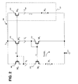
- FIG. 2 illustrates a conventional bias generation circuit 200 for maintaining a constant transcondutance despite temperature changes and process variations.
- the bias generation circuit includes a pair of NMOS transistors 210 and 220 serially to a pair of PMOS transistors 230 and 240 between a positive voltage source (V dd ) and ground.
- NMOS transistor 210 has a source coupled to ground (GND), and a gate and drain coupled to each other.
- the drain of NMOS transistor 210 is further coupled to the drain of the PMOS transistor 230 and the gate of NMOS transistor 210 is also coupled to the gate of NMOS transistor 220.
- the source of the second NMOS transistor 220 is coupled via a resistor R 1 to ground and its drain is coupled to the drain of the PMOS transistor 240.
- the two PMOS transistors 230 and 240 are coupled at their sources to a constant voltage source V dd and at their gates to each other.
- the PMOS transistors 230 and 240 form a current mirror for driving the NMOS transistors 210 and 220.
- PMOS transistors 230 and 240 are integrated devices, having similar characteristics.
- the drain source junction (V ds ) of PMOS transistor 230 equals the drain source voltage V ds of device 240. Therefore, the currents through the devices (I 1 and I 2 ) are essentially equal because the gates of the PMOS transistors 230 and 240 are at equal potential, that is, they are coupled together.
- the bias generation circuit 200 In operation the bias generation circuit 200 generates a bias current that is inversely proportional to the resistance of the setting resistor R 1 .
- a PMOS transistor 260 transfers the bias current to a load, (illustrated, by way of example, as a resistive load R 0 ).
- the gate to source voltage of NMOS transistor 210 is given by Eq.(2).
- the transconductance parameter ⁇ : n C ox (W/L)
- C ox is the oxide capacitance per unit area
- W/L is the aspect ratio of NMOS transistor 210. Therefore the drain current for NMOS transistor 210 is given by Eq.(3).
- the transconductance of the PMOS current source transistor 260 is inversely proportional to the resistance of resistor R 1 .
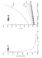
- FIG. 3 is a graphical illustration of the resultant output current I out versus temperature for the temperature dependent bias generation circuit 200.
- the illustrated embodiment of the temperature dependent bias generation circuit 200 generates an output current with a temperature coefficient of approximately 2,000 ppm/°C (i.e. current varies approximately 20% for a 100 degree change in temperature).
- the temperature coefficient of conventional temperature dependent bias generation circuits may not be large enough to provide sufficient temperature compensation.
- the output load for high frequency tuned applications is typically an inductor whose effective series resistance has a relatively high temperature coefficient. Therefore, the effective impedance of the inductive load varies with temperature as does the resulting transconductance of the device. This may result in relatively large gain variation with varying temperature that may'not be compensated for by conventional bias generation circuits alone.
- an exemplary embodiment of the present invention comprises, by way of example, a bias generation circuit having a variable resistance device coupled to a temperature dependent bias generation circuit to generate a high temperature coefficient current that may be used to compensate for temperature induced variations in the performance of analog MOSFET circuits.
- the described exemplary bias generation circuit 400 comprises a MOS triode transistor 410 coupled in series with NMOS transistor 210 and ground.
- the gate of the triode transistor is coupled to a positive voltage source, such as, for example V dd , the level of which is chosen to ensure that triode transistor 410 operates in the triode region.
- the on resistance and drain-source voltage (V ds ) of the triode transistor 410 increase with increasing temperature.
- the dependence of V ds on temperature varies as a function of device size (width).
- the change in V ds as a function of temperature increases as the width of the triode transistor 410 decreases. Therefore, the voltage at node N 1 coupled between the drain of the triode device 410 and source of the NMOS transistor 230 also increases as a function of increasing temperature. Further the voltage at node N 1 increases more as a function of increasing temperature as the size of the triode transistor 410 decreases.
- FIG. 5 graphically illustrates the voltage at node N 1 as a function of temperature for triode transistor widths ranging from nine microns to one micron.
- the voltage at node N 1 increases in an approximately linear fashion with increasing temperature for device sizes greater than about two microns.
- the voltage at node N 1 increases over a greater range in a non-linear fashion with increasing temperature for a device width of one micron. Therefore, the temperature dependent voltage at node N 2 can be controlled by varying the size of the triode device 410.
- the drain current of the output leg of the bias generation circuit can be defined as follows in Eq (5): ID ⁇ 3 2 ⁇ nCox ( W / L ) R 1 - 1 ⁇ nCox ( W / L ) t ( V gs - V t t ) 2 where V gs is the gate source voltage of the triode device 410, (W/L) t is the aspect ratio of the triode device 410 and V tt is the threshold voltage of the triode device.
- the drain current of NMOS transistor 210 increases with decreasing device size.
- the effective on resistance approximately equal to 1/: n C ox (W/L) t (V gs -V tt )
- the voltage drop across the drain to source junction of the triode device approaches zero. Therefore, the drain current converges to the conventional solution provided by the bias generation circuit of FIG. 2 as the width of the triode device converges to infinity.
- the effective on-resistance of the triode device increases, increasing the drain current of the bias generation circuit.
- FIG. 6 graphically illustrates the output current I out of bias generation circuit 400 (see FIG. 4) as a function of temperature for triode device widths ranging from one micron to nine microns.
- the output current of the described exemplary bias generation circuit increases on the order of about 5-10 mA over a 100 °C temperature increase for triode devices having a width between nine microns and two microns.
- the output current of the described exemplary bias generation circuit increases on the order of about 60 mA over 100 °C temperature increase for a one micron triode device.
- FIG. 7 graphically illustrates the corresponding effective temperature coefficient of the described exemplary bias generation circuit as a function of the size (width) of triode device 410.
- the effective temperature coefficient of the bias generation circuit for a triode device having a one micron width is in the range of about 14,000 PPM.
- the described exemplary bias generation circuit generates a current with a temperature coefficient that converges to that provided by the conventional bias generation circuit of FIG. 2.
- the width or aspect ratio of the triode device may be dynamically controlled to generate a current with a relatively wide dynamic range of temperature coefficient performance.
- a multi-stage system comprising a plurality of parallel triodes may be dynamically switched on and off to provide a desired aspect ratio and corresponding output current as a function of temperature.
- the high temperature coefficient bias current at least partially compensates for process variations which may further improve the performance of MOS circuits formed from devices having slow-MOS process corners.
- a process corner is a particular set of conditions related to processing involved in the manufacture and fabrication of an integrated circuit. A variation of process exists from the manufacture of one lot of chips to the manufacture of a second lot of chips. Process corners include slow process corners where the active MOS devices sink less current and therefore provide less gain.
- the loss of gain may be compensated for by increasing the bias current as the process moves toward a slow corner.
- the on resistance of the triode device is proportional to process. Therefore, the on resistance increases for a slow process, increasing the output current of the bias generation circuit and compensating for the reduced gain of the analog device.
- the described exemplary high temperature coefficient bias generation circuit may be integrated into any of a variety of RF circuit applications.
- the described exemplary bias generation circuit may be incorporated into the transmit node 802 or receive node 810 of a typical communication system 800 for transmitting a radio frequency information signal 805 to a receive node 810 that receives and processes the transmitted RF information signal.
- an exemplary transmit node 802 includes, by way of example, a transmitter processing module 920 that receives and processes outbound data in accordance with one or more communication standards, including but not limited to, IEEE 802.11, Bluetooth, advanced mobile phone services (AMPS), global systems for mobile communications (GSM), code division multiple access (CDMA), local multi-point distribution systems (LMDS), multi-channel-multi-point distribution systems (MMDS), and or variations thereof.
- the transmitter processing module may execute a variety of transmitter functions such as for example, scrambling, encoding, constellation mapping, and modulation to produce digital transmitter data 920(a) formatted in accordance with the appropriate communication standard.
- the transmitter processing module may be implemented using a shared processing device, individual processing device, or a plurality of processing devices.
- the processing module may comprise, a microprocessor, microcontroller, digital signal processor, microcomputer, central processing unit, state machine, or any other device that manipulates signals based upon operational instructions.
- a digital to analog converter (DAC) 930 receives the digital transmitter data from the transmitter processing module and converts the digital transmitter data from the digital domain to the analog domain.
- the analog transmitter data is a IF or baseband signal typically in the frequency range of one hundred kilohertz to a few megahertz.
- the analog transmitter data is forwarded to a filter stage 940 that filters the analog IF or baseband signal to attenuate unwanted out of band signals to produce a filtered IF signal that is coupled to an up-converter 950.
- the up-converter 950 converts the filtered analog IF or baseband signal into an RF signal based on a transmitter local oscillator signal provided by a local oscillator 960.
- An exemplary power amplifier 970 biased by the described exemplary high temperature coefficient bias generation circuit may adjust the gain and amplify the RF signal to produce an outbound RF signal 970(a) which is coupled to an antennae 980 for transmission to one or more receiver nodes.
- the present invention is not limited to RF amplifier applications. Rather, the present invention may generally be used to bias any inductive MOS load that has sufficient headroom to support the large temperature coefficient current provided by the described exemplary bias generation circuit.
- the present invention is not limited to the use of an NMOS triode transistor serially coupled between the output leg of a Widlar current source and ground. Rather, the present invention may utilize a PMOS triode transistor or other devices having a resistance that varies with temperature such that the output current of the bias generation circuit increases with increasing resistance of the variable resistance device. It is the applicant's intention to cover by claims all such uses of the invention and those changes and modifications that could be made to the embodiments of the invention herein chosen for the purpose of disclosure without departing from the spirit and scope of the invention.
Landscapes
- Engineering & Computer Science (AREA)
- Microelectronics & Electronic Packaging (AREA)
- Physics & Mathematics (AREA)
- Nonlinear Science (AREA)
- Electromagnetism (AREA)
- General Physics & Mathematics (AREA)
- Radar, Positioning & Navigation (AREA)
- Automation & Control Theory (AREA)
- Amplifiers (AREA)
- Networks Using Active Elements (AREA)
Applications Claiming Priority (2)
| Application Number | Priority Date | Filing Date | Title |
|---|---|---|---|
| US10/447,790 US6946896B2 (en) | 2003-05-29 | 2003-05-29 | High temperature coefficient MOS bias generation circuit |
| US447790 | 2003-05-29 |
Publications (3)
| Publication Number | Publication Date |
|---|---|
| EP1482390A2 true EP1482390A2 (fr) | 2004-12-01 |
| EP1482390A3 EP1482390A3 (fr) | 2005-01-05 |
| EP1482390B1 EP1482390B1 (fr) | 2010-09-22 |
Family
ID=33131596
Family Applications (1)
| Application Number | Title | Priority Date | Filing Date |
|---|---|---|---|
| EP04007356A Expired - Lifetime EP1482390B1 (fr) | 2003-05-29 | 2004-03-26 | Circuit de polarisation de MOS à haute coefficient de température |
Country Status (3)
| Country | Link |
|---|---|
| US (1) | US6946896B2 (fr) |
| EP (1) | EP1482390B1 (fr) |
| DE (1) | DE602004029220D1 (fr) |
Cited By (1)
| Publication number | Priority date | Publication date | Assignee | Title |
|---|---|---|---|---|
| WO2008043845A1 (fr) * | 2006-10-13 | 2008-04-17 | Austriamicrosystems Ag | Arrangement de circuit comprenant une source de courant de polarisation et procédé de fonctionnement d'un arrangement de circuit |
Families Citing this family (13)
| Publication number | Priority date | Publication date | Assignee | Title |
|---|---|---|---|---|
| US7372316B2 (en) * | 2004-11-25 | 2008-05-13 | Stmicroelectronics Pvt. Ltd. | Temperature compensated reference current generator |
| KR100657171B1 (ko) * | 2005-04-29 | 2006-12-20 | 삼성전자주식회사 | 리프레쉬 제어회로 및 리프레쉬 제어방법 |
| US9455722B2 (en) * | 2005-11-30 | 2016-09-27 | Ati Technologies Ulc | Method and apparatus for fast locking of a clock generating circuit |
| JP5107272B2 (ja) * | 2009-01-15 | 2012-12-26 | 株式会社東芝 | 温度補償回路 |
| US8575998B2 (en) * | 2009-07-02 | 2013-11-05 | Taiwan Semiconductor Manufacturing Company, Ltd. | Voltage reference circuit with temperature compensation |
| US8669808B2 (en) * | 2009-09-14 | 2014-03-11 | Mediatek Inc. | Bias circuit and phase-locked loop circuit using the same |
| US8985850B1 (en) * | 2009-10-30 | 2015-03-24 | Cypress Semiconductor Corporation | Adaptive gate driver strength control |
| US7990223B1 (en) * | 2010-05-31 | 2011-08-02 | Kabushiki Kaisha Toshiba | High frequency module and operating method of the same |
| US8451047B2 (en) * | 2011-05-17 | 2013-05-28 | Issc Technologies Corp. | Circuit used for indicating process corner and extreme temperature |
| US9385694B2 (en) * | 2011-12-20 | 2016-07-05 | Conexant Systems, Inc. | Low-power programmable oscillator and ramp generator |
| KR20150104297A (ko) * | 2014-03-05 | 2015-09-15 | 에스케이하이닉스 주식회사 | 반도체 장치 및 반도체 시스템 |
| JP2016121907A (ja) * | 2014-12-24 | 2016-07-07 | 株式会社ソシオネクスト | 温度センサ回路及び集積回路 |
| US20250362701A1 (en) * | 2024-05-23 | 2025-11-27 | Taiwan Semiconductor Manufacturing Company, Ltd. | Voltage reference circuit |
Citations (1)
| Publication number | Priority date | Publication date | Assignee | Title |
|---|---|---|---|---|
| US6271710B1 (en) | 1995-06-12 | 2001-08-07 | Mitsubishi Denki Kabushiki Kaisha | Temperature dependent circuit, and current generating circuit, inverter and oscillation circuit using the same |
Family Cites Families (14)
| Publication number | Priority date | Publication date | Assignee | Title |
|---|---|---|---|---|
| US4743862A (en) | 1986-05-02 | 1988-05-10 | Anadigics, Inc. | JFET current mirror and voltage level shifting apparatus |
| US4959622A (en) | 1989-08-31 | 1990-09-25 | Delco Electronics Corporation | Operational amplifier with precise bias current control |
| US5157285A (en) | 1991-08-30 | 1992-10-20 | Allen Michael J | Low noise, temperature-compensated, and process-compensated current and voltage control circuits |
| US5349286A (en) * | 1993-06-18 | 1994-09-20 | Texas Instruments Incorporated | Compensation for low gain bipolar transistors in voltage and current reference circuits |
| JP3039611B2 (ja) | 1995-05-26 | 2000-05-08 | 日本電気株式会社 | カレントミラー回路 |
| US5892388A (en) * | 1996-04-15 | 1999-04-06 | National Semiconductor Corporation | Low power bias circuit using FET as a resistor |
| US6107868A (en) * | 1998-08-11 | 2000-08-22 | Analog Devices, Inc. | Temperature, supply and process-insensitive CMOS reference structures |
| US6323725B1 (en) | 1999-03-31 | 2001-11-27 | Qualcomm Incorporated | Constant transconductance bias circuit having body effect cancellation circuitry |
| JP3289276B2 (ja) | 1999-05-27 | 2002-06-04 | 日本電気株式会社 | 半導体装置 |
| EP1081477B1 (fr) * | 1999-08-31 | 2006-10-18 | STMicroelectronics S.r.l. | Capteur de température en technologie Cmos |
| KR100368982B1 (ko) * | 1999-11-30 | 2003-01-24 | 주식회사 하이닉스반도체 | 씨모스 정전류 레퍼런스 회로 |
| US6407623B1 (en) | 2001-01-31 | 2002-06-18 | Qualcomm Incorporated | Bias circuit for maintaining a constant value of transconductance divided by load capacitance |
| EP1315063A1 (fr) * | 2001-11-14 | 2003-05-28 | Dialog Semiconductor GmbH | Référence de courant indépendante de la tension de seuil d'un transistor MOS |
| JP4017464B2 (ja) * | 2002-07-15 | 2007-12-05 | 沖電気工業株式会社 | 基準電圧回路 |
-
2003
- 2003-05-29 US US10/447,790 patent/US6946896B2/en not_active Expired - Fee Related
-
2004
- 2004-03-26 DE DE602004029220T patent/DE602004029220D1/de not_active Expired - Lifetime
- 2004-03-26 EP EP04007356A patent/EP1482390B1/fr not_active Expired - Lifetime
Patent Citations (1)
| Publication number | Priority date | Publication date | Assignee | Title |
|---|---|---|---|---|
| US6271710B1 (en) | 1995-06-12 | 2001-08-07 | Mitsubishi Denki Kabushiki Kaisha | Temperature dependent circuit, and current generating circuit, inverter and oscillation circuit using the same |
Cited By (1)
| Publication number | Priority date | Publication date | Assignee | Title |
|---|---|---|---|---|
| WO2008043845A1 (fr) * | 2006-10-13 | 2008-04-17 | Austriamicrosystems Ag | Arrangement de circuit comprenant une source de courant de polarisation et procédé de fonctionnement d'un arrangement de circuit |
Also Published As
| Publication number | Publication date |
|---|---|
| US20040239404A1 (en) | 2004-12-02 |
| US6946896B2 (en) | 2005-09-20 |
| EP1482390A3 (fr) | 2005-01-05 |
| EP1482390B1 (fr) | 2010-09-22 |
| DE602004029220D1 (de) | 2010-11-04 |
Similar Documents
| Publication | Publication Date | Title |
|---|---|---|
| KR100830361B1 (ko) | 능동 바이어스 회로 | |
| EP0854570B1 (fr) | Circuit pour stabiliser la polarisation | |
| US6888411B2 (en) | Radio frequency variable gain amplifier with linearity insensitive to gain | |
| US6989705B2 (en) | High linearity passive mixer and associated LO buffer | |
| US6946896B2 (en) | High temperature coefficient MOS bias generation circuit | |
| US11264962B2 (en) | Fully differential amplifier including feedforward path | |
| KR100614928B1 (ko) | 선형화를 위한 미분 중첩회로 | |
| US12500559B2 (en) | Differential buffer circuit | |
| KR100979896B1 (ko) | 자동바이어싱 공급 규제를 가지는 가변 이득 증폭기 | |
| EP2582042A1 (fr) | Circuit d'amplificateur à faible bruit | |
| US6252460B1 (en) | FET balun transformer | |
| US20220393655A1 (en) | Linearization using complementary devices | |
| US20130029627A1 (en) | Amplifier and associated receiver | |
| JP2003188653A (ja) | 無線通信用電子部品および通信用半導体集積回路 | |
| US7737785B2 (en) | Amplifier circuit with adjustable amplification | |
| US12341475B2 (en) | Semiconductor device | |
| CN110661494A (zh) | 高频放大电路及半导体设备 | |
| US20250062730A1 (en) | Linearization using fets with designable pinch off voltage | |
| US20220294399A1 (en) | Semiconductor device | |
| JP3176793B2 (ja) | 増幅回路 | |
| US6992530B2 (en) | RF amplifier with improved impedance matching | |
| CN117459000A (zh) | 用于低噪声放大器的偏置电路以及射频低噪声放大器 | |
| JP2001237650A (ja) | 利得可変型増幅器 | |
| JP2003224431A (ja) | 位相歪補正増幅器 | |
| KR20050016695A (ko) | 반도체 집적 회로 및 반도체 집적 회로의 제조방법 |
Legal Events
| Date | Code | Title | Description |
|---|---|---|---|
| PUAI | Public reference made under article 153(3) epc to a published international application that has entered the european phase |
Free format text: ORIGINAL CODE: 0009012 |
|
| PUAL | Search report despatched |
Free format text: ORIGINAL CODE: 0009013 |
|
| AK | Designated contracting states |
Kind code of ref document: A2 Designated state(s): AT BE BG CH CY CZ DE DK EE ES FI FR GB GR HU IE IT LI LU MC NL PL PT RO SE SI SK TR |
|
| AX | Request for extension of the european patent |
Extension state: AL LT LV MK |
|
| AK | Designated contracting states |
Kind code of ref document: A3 Designated state(s): AT BE BG CH CY CZ DE DK EE ES FI FR GB GR HU IE IT LI LU MC NL PL PT RO SE SI SK TR |
|
| AX | Request for extension of the european patent |
Extension state: AL LT LV MK |
|
| 17P | Request for examination filed |
Effective date: 20050705 |
|
| AKX | Designation fees paid |
Designated state(s): DE FR GB |
|
| 17Q | First examination report despatched |
Effective date: 20061017 |
|
| RAP1 | Party data changed (applicant data changed or rights of an application transferred) |
Owner name: BROADCOM CORPORATION |
|
| GRAP | Despatch of communication of intention to grant a patent |
Free format text: ORIGINAL CODE: EPIDOSNIGR1 |
|
| GRAS | Grant fee paid |
Free format text: ORIGINAL CODE: EPIDOSNIGR3 |
|
| GRAA | (expected) grant |
Free format text: ORIGINAL CODE: 0009210 |
|
| AK | Designated contracting states |
Kind code of ref document: B1 Designated state(s): DE FR GB |
|
| REG | Reference to a national code |
Ref country code: GB Ref legal event code: FG4D |
|
| REF | Corresponds to: |
Ref document number: 602004029220 Country of ref document: DE Date of ref document: 20101104 Kind code of ref document: P |
|
| PLBE | No opposition filed within time limit |
Free format text: ORIGINAL CODE: 0009261 |
|
| STAA | Information on the status of an ep patent application or granted ep patent |
Free format text: STATUS: NO OPPOSITION FILED WITHIN TIME LIMIT |
|
| 26N | No opposition filed |
Effective date: 20110623 |
|
| REG | Reference to a national code |
Ref country code: DE Ref legal event code: R097 Ref document number: 602004029220 Country of ref document: DE Effective date: 20110623 |
|
| REG | Reference to a national code |
Ref country code: FR Ref legal event code: ST Effective date: 20111130 |
|
| PG25 | Lapsed in a contracting state [announced via postgrant information from national office to epo] |
Ref country code: FR Free format text: LAPSE BECAUSE OF NON-PAYMENT OF DUE FEES Effective date: 20110331 |
|
| PGFP | Annual fee paid to national office [announced via postgrant information from national office to epo] |
Ref country code: GB Payment date: 20130318 Year of fee payment: 10 Ref country code: DE Payment date: 20130331 Year of fee payment: 10 |
|
| REG | Reference to a national code |
Ref country code: DE Ref legal event code: R119 Ref document number: 602004029220 Country of ref document: DE |
|
| GBPC | Gb: european patent ceased through non-payment of renewal fee |
Effective date: 20140326 |
|
| REG | Reference to a national code |
Ref country code: DE Ref legal event code: R119 Ref document number: 602004029220 Country of ref document: DE Effective date: 20141001 |
|
| PG25 | Lapsed in a contracting state [announced via postgrant information from national office to epo] |
Ref country code: GB Free format text: LAPSE BECAUSE OF NON-PAYMENT OF DUE FEES Effective date: 20140326 Ref country code: DE Free format text: LAPSE BECAUSE OF NON-PAYMENT OF DUE FEES Effective date: 20141001 |