EP1482635A2 - Chaíne d'émission réception et procédé d'émission - Google Patents
Chaíne d'émission réception et procédé d'émission Download PDFInfo
- Publication number
- EP1482635A2 EP1482635A2 EP04018081A EP04018081A EP1482635A2 EP 1482635 A2 EP1482635 A2 EP 1482635A2 EP 04018081 A EP04018081 A EP 04018081A EP 04018081 A EP04018081 A EP 04018081A EP 1482635 A2 EP1482635 A2 EP 1482635A2
- Authority
- EP
- European Patent Office
- Prior art keywords
- frequency
- signal
- loop
- mhz
- translation
- Prior art date
- Legal status (The legal status is an assumption and is not a legal conclusion. Google has not performed a legal analysis and makes no representation as to the accuracy of the status listed.)
- Granted
Links
Images

Classifications
-
- H—ELECTRICITY
- H03—ELECTRONIC CIRCUITRY
- H03C—MODULATION
- H03C3/00—Angle modulation
- H03C3/02—Details
- H03C3/09—Modifications of modulator for regulating the mean frequency
- H03C3/0908—Modifications of modulator for regulating the mean frequency using a phase locked loop
- H03C3/0916—Modifications of modulator for regulating the mean frequency using a phase locked loop with frequency divider or counter in the loop
- H03C3/0925—Modifications of modulator for regulating the mean frequency using a phase locked loop with frequency divider or counter in the loop applying frequency modulation at the divider in the feedback loop
-
- H—ELECTRICITY
- H03—ELECTRONIC CIRCUITRY
- H03C—MODULATION
- H03C3/00—Angle modulation
- H03C3/02—Details
- H03C3/09—Modifications of modulator for regulating the mean frequency
- H03C3/0908—Modifications of modulator for regulating the mean frequency using a phase locked loop
- H03C3/0966—Modifications of modulator for regulating the mean frequency using a phase locked loop modulating the reference clock
-
- H—ELECTRICITY
- H03—ELECTRONIC CIRCUITRY
- H03D—DEMODULATION OR TRANSFERENCE OF MODULATION FROM ONE CARRIER TO ANOTHER
- H03D7/00—Transference of modulation from one carrier to another, e.g. frequency-changing
- H03D7/16—Multiple-frequency-changing
- H03D7/161—Multiple-frequency-changing all the frequency changers being connected in cascade
- H03D7/163—Multiple-frequency-changing all the frequency changers being connected in cascade the local oscillations of at least two of the frequency changers being derived from a single oscillator
-
- H—ELECTRICITY
- H03—ELECTRONIC CIRCUITRY
- H03L—AUTOMATIC CONTROL, STARTING, SYNCHRONISATION OR STABILISATION OF GENERATORS OF ELECTRONIC OSCILLATIONS OR PULSES
- H03L7/00—Automatic control of frequency or phase; Synchronisation
- H03L7/06—Automatic control of frequency or phase; Synchronisation using a reference signal applied to a frequency- or phase-locked loop
- H03L7/16—Indirect frequency synthesis, i.e. generating a desired one of a number of predetermined frequencies using a frequency- or phase-locked loop
-
- H—ELECTRICITY
- H03—ELECTRONIC CIRCUITRY
- H03L—AUTOMATIC CONTROL, STARTING, SYNCHRONISATION OR STABILISATION OF GENERATORS OF ELECTRONIC OSCILLATIONS OR PULSES
- H03L7/00—Automatic control of frequency or phase; Synchronisation
- H03L7/06—Automatic control of frequency or phase; Synchronisation using a reference signal applied to a frequency- or phase-locked loop
- H03L7/16—Indirect frequency synthesis, i.e. generating a desired one of a number of predetermined frequencies using a frequency- or phase-locked loop
- H03L7/22—Indirect frequency synthesis, i.e. generating a desired one of a number of predetermined frequencies using a frequency- or phase-locked loop using more than one loop
- H03L7/23—Indirect frequency synthesis, i.e. generating a desired one of a number of predetermined frequencies using a frequency- or phase-locked loop using more than one loop with pulse counters or frequency dividers
Definitions
- the present invention relates to a reception transmission chain and a transmission method usable in particular in the field of mobile telephony.
- the preferred field of the invention is that of mobile telephony because, in mobile telephony, of TDMA as well as FDMA type, it is necessary to regularly cause jumps in transmission frequency. From the point of view of the mobile telephone system, these jumps are used to change the channel and therefore to distribute the noise present in particular frequency bands between several communications exchanged between mobile telephones and base stations.
- the invention therefore aims to allow frequency agility. As such, it could also be used in the radar field, as a countermeasure for example.
- Transmission channels generally include a set of phase locked loops. Each phase locked loop is provided with an oscillator which is voltage controlled.
- the principle of these emission chains is to mix the waves produced by the phase locked loops so as to produce an emission wave.
- a first loop is produced, the oscillator of which oscillates at an intermediate frequency, for example around 100 or 200 MHz, and a second loop, the oscillator of which oscillates at a translation frequency.
- the translation frequency may be of the order of 800 MHz to lead to a transmission around 900 MHz.
- Within the framework of the DCS it will be of the order of 1700 MHz to lead to a transmission around 1800 MHz.
- the combination of these two waves at intermediate frequency and at translation frequency is generally direct. It can also be performed as part of a third loop.
- the signal from the intermediate frequency loop then serves as a setpoint for a phase comparator of the third loop which receives a signal resulting from the subtraction of the signal at the translation frequency from a signal at a transmission frequency.
- a phase locked loop essentially has an oscillator variable frequency controlled in voltage, connected at the output to the input of a divider frequency.
- the output of the frequency divider is connected to the input of a phase comparator which also receives a setpoint signal at a frequency to respect.
- the phase comparator delivers a control signal which, from preferably, is filtered in a low pass filter.
- the control signal issued by the low pass filter is used to control the voltage controlled oscillator.
- Frequency hopping corresponding to multiples of a width of normalized channel strip, are multiples of normalized values.
- 200 KHz channel bandwidths are used.
- the different channels are thus spaced from each other at an equal frequency step at 200 KHz.
- the division coefficient of the divider incorporated in the loop frequency translation so as to cause jumps by addition / subtraction expected.
- the division coefficient is around 8500. This coefficient varies by one or more units depending on whether the jump frequency to be achieved is one or more times the step of 200 KHz.
- a first step of variation will be worth 5.2 MHz with a comparison frequency of 2.6 MHz.
- Another step will be worth 5 MHz with a comparison frequency of 1 MHz.
- the division coefficient of the divisor of the translation frequency loop can go from approximately 8500 to 600.
- the loops at phase lock must reach the new frequency value the most quickly possible.
- the speed of rallying of the servo is proportional to the width of the pass band of the low pass filter connected to the comparator output. Because the comparison frequency is much more high with the invention, it is possible to have a much cutoff frequency higher. With a much higher filter cutoff frequency, the time rallying is lower. With the invention this speed is then significantly stronger and rallying is faster due to a frequency of much larger comparison chosen from the loops themselves for frequency hopping.
- the invention therefore also relates to a transmission and reception chain, in particular for a mobile telephone, comprising, interconnected, a first, second and third phase locked loop, for respectively produce a signal at an intermediate frequency, a signal at a translation frequency and a signal at a transmission frequency, the value of the emission frequency being equal to the sum of the frequency values intermediate and translational, characterized in that the translational loop is split into first and second translation loops to serve respectively in a transmission circuit and in a reception circuit, each of these two loops comprising in series a variable frequency oscillator voltage controlled, a frequency divider, a phase comparator and a low pass filter.
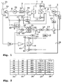
- FIG. 1 shows a transmission chain according to the invention.
- This emission chain is especially intended for use in the field of mobile telephony.
- This chain has three phase locked loops noted 1 to 3.
- the first loop 1 is a so-called intermediate frequency loop and it produces at its output 4 a signal at an intermediate frequency.
- the second loop 2 is a loop at a translation frequency and produces at its output 5 a signal at a translation frequency.
- the third loop is the send loop, it produces at its output 6 a signal at a transmission frequency.
- the signal available at output 4 will have a frequency of the order of 100 MHz, that available at output 5 will have a frequency of around 1700 MHz.
- the value of the emission frequency is thus additively formed by the value of the frequency intermediate and translational frequency.
- the frequency transmission is therefore of the order of 1800 MHz (with variations depending on the frequency allocations granted to a telecommunications operator). In GSM framework these values must be modified so that the frequency 900 MHz emission range.
- the transmission frequency by a subtraction, by the value of the intermediate frequency, of the value of the translation frequency.
- the terminology of additive formation since the translation frequency would then be the result of the addition of the transmission frequency and the intermediate frequency.
- the emission chain of the invention also includes a circuit modulator 7 interposed in the connections between these loops.
- the modulator circuit 7 is interposed in the connection between loop 1 and loop 3. It could nevertheless be interposed between any loops.
- the aim is to modulate the signal available at the transmission frequency by a signal modulating to transmit.
- the modulating signal to be transmitted represents the information. It is here an analog signal with two components I and Q (as well as its values NI and NQ).
- the intermediate frequency signal available at the output 4 is introduced on a phase shifter by 90 degrees 8 whose outputs, 90 ° out of phase with each other, attacking mixers 9 and 10.
- the 90 ° phase shifter comprises a double divider of frequency by two triggered respectively by a rising edge and an edge falling from the intermediate frequency signal.
- the frequency of the signal the selected intermediate frequency is, for this reason, double that mentioned so far.
- this clarification does not detract from the generality of the invention since it is enough for the realization of the chain of the invention to double all the values relating to the first loop.
- 90 ° phase shifted components of the signal at intermediate frequency mix with the I and Q signals respectively.
- the outputs of mixers 9 and 10 are combined together in an adder 11 which delivers a modulated signal.
- modulator circuit Any other type of modulator circuit would of course be possible. In particular, the place of this modulator circuit could be different. In some case, the modulator circuit is placed in the transmission loop
- the frequency setting of loops 1 and 2 is obtained by the production of a reference signal produced by a reference circuit 12.
- the signal produced by reference 12 has a freight frequency of 13 MHz. This signal could however have any other value.
- the circuit 12 of reference comprises a quartz.
- the signal of reference 12 is introduced, in particular by dividers 13 and 14, of value Mi and Ms, on the input inputs of phase comparators 15 and 16 of loops 1 and 2 respectively.
- the phase 15 and 16 comparators also receive output signals delivered by two voltage controlled oscillators 17 and 18 of these loops and which have been divided by divisors 19 and 20 of value Ni and Ns in loops 1 and 2 respectively.
- the signal available at the output of the divider 13 will then have a frequency of 1 MHz.
- the signal delivered by the phase comparator 15 will therefore control oscillator 17 so that the result of the division by Ni of the signal produced by this oscillator 17 is also a signal at 1 MHz. Consequently, the signal available on output 4 will have a Ni frequency x 1MHz.
- the operation of a loop is output a signal whose frequency is the product of the frequency of the setpoint signal by the division coefficient of the loop.
- the oscillator 17 comprises, in a known manner, an output connected to the input of the divider 19 and at the input of the modulator circuit 7. This output delivers the signal to the intermediate frequency.
- the frequency of the frequency translation loop 2 setpoint signal had to must be displayed at this low value.
- the coefficient Ns of divisor 20 was high. In an example it was worth 8500 for transform a signal at 1700 MHz into a signal with a frequency comparable to 200 KHz.
- the transmit frequency available at output 6 is the result of adding the signal frequency available at output 4 with the signal frequency available at output 5.
- the intermediate frequency regulation loop 1 had a fixed value in frequency.
- the signal available in this loop has a frequency which varies during frequency jumps.
- the addition of the two signals is preferably caused in the third loop 3 as follows.
- the loop 3 also includes an oscillator 21 voltage controlled.
- the output 6 of the oscillator 21 is connected to a device transmission comprising an amplifier 23, a duplexer 24 and an overhead 25.
- the signal available at output 6 is also picked up by a sensor 26 before amplification.
- This sampled signal is mixed in a mixer 27 with the signal available at output 5 of loop 2.
- the signal resulting from the mixing by the mixer 27, available at an outlet 28 is injected into a phase comparator 29 where it is compared to the signal delivered by the chain 7, therefore, with regard to the carrier of the transmission frequency, by the intermediate frequency loop 1.
- the mixer 27 performs the subtraction and adding the frequencies of the signals available at output 6 and output 5. With a low pass filter 33, the addition component is eliminated.
- the signal delivered by the comparator 29 which controls the oscillator 21 has the effect that the result of this subtraction must be equal to the signal at the intermediate frequency, to the signal modulation I and
- the phase comparators 15, 16 and 29 are connected to the oscillators voltage controlled 17, 18 and 21 via low pass filters respectively 30, 31 and 32.
- the filter 30 has a low cut-off frequency of around 100 KHz.
- Filter 31 has a low cut-off frequency of around 100 at 200 KHz.
- Filter 32 has a low cut-off frequency of the order of 200 to 300 KHz.
- the cut-off frequency of the filter 33 is of the order of 200 MHz.
- the filters 30 to 33 are loop filters.
- the dividers 13 14, 19 and 20 are essentially programmable. We easily know how to make such dividers using in their principles of counters with automatic reset and retriggering as soon as that they have reached a prerecorded value.
- the re-trigger signal of these counters represents the divided frequency signal.
- the pre-recorded value represents the division coefficient.
- FIG. 2 shows a table making it possible to explain, in a quantified manner, simply, the operation of the invention.
- a first column 34 indicates possible values of the division coefficient Ni of the divider 19.
- a second column 35 indicates the value of the intermediate frequency available in consequence at exit 4.
- a third column 36 gives the value of the coefficient divider 20.
- a fourth column 37 indicates the frequency of the signal at the translation frequency available at output 5.
- a last column 38 indicates the value of the frequency of the resulting transmission signal.
- the coefficient Mi of divider 13 is equal to 13 so that the frequency of the setpoint signal admitted to the comparator 15 input is worth 1 MHz. But the explanation remains valid if this coefficient Mi has a different value.
- the coefficient Ni is fixed at the value 98
- the frequency of the signal introduced on the other input of comparator 15 will be worth the value of the frequency delivered by the oscillator 17 divided by 98.
- a times compared by comparator 15, then filtered by filter 30, the signal resulting from the comparison is fed back as a command to oscillator 17.
- the frequency of the signal available at output 4 is a signal at one 98 MHz frequency (98x1 MHz).
- the divider 14 has a division coefficient Ms equal to 5. He too could have another value, however.
- the signal allowed on the setpoint input of phase comparator 16 is 2.6 MHz.
- the signal available at output 5 of oscillator 18 will be worth this setpoint, 2.6 MHz, multiplied by the coefficient Ms.
- the variations in the division coefficients Ni and Ns are linked by a variation in the transmission frequency.
- the step A of variation of the coefficient Ni is 5, it causes a step "a" of frequency variation of the 5 MHz intermediate frequency.
- a step B of 2 units of Ns causes a step of frequency "b" of 5.2 MHz of the frequency of translation.
- the transmission frequency then changes with a frequency step b-a, equal to 200 KHz in the example.
- the translation frequency Ft is equal to FrefxNs / Ms.
- the frequency intermediate Fi is FrefxNi / Mi.
- b Frefx ⁇ Ns / Ms
- a Frefx ⁇ Ni / Mi.
- ⁇ Ns is the step B then that ⁇ Ni is the step A.
- a / b (B / Ms) / (A / Mi).
- the Mi / Ms ratio of the divisor coefficients of the divisors 13 and 14 respectively is equal or proportional to Ab / aB.
- the coefficient Ni could go down to 1.
- the frequency steps a and b can be combined differently.
- sixth line of the table it is possible to arrive at the transmission frequency of 1711 MHz in two ways. Let the coefficient Ni be 73 and the coefficient Ns be 630, in logical continuation of the variation of these coefficients in the columns 34 and 36 respectively. Or, preferably, the coefficient Ni is equal to 99 while the coefficient Ns is 620. In this case, we also arrive at the desired result, but with a limited exploration of the coefficient Ni. We thus play on modulo values a and modulo b to produce a result modulo a - modulo b, or modulo a + modulo b which allows a limited excursion of the coefficient Ni.
- Figure 1 also schematically shows another characteristic important of the invention represented in the form of a gray area 39.
- the shaded area 39 shows all the modulator equipment which can be integrated on the same integrated circuit. Apart from filters 30 to 33 and as well as voltage controlled oscillators 18 and 21, all circuits to date can be integrated on the same integrated circuit 39. This leads to having a architecture at very low cost. Even oscillator 17 can be integrated on the circuit integrated 39.
- a frequency divider 40 by two is placed in cascade.
- the divider 40 is switchable. It allows to divide, or not to divide, by two the frequency of signal at the translation frequency. In practice, such a divider 40 can allow to switch from the DCS protocol (1800 MHz) to the GSM protocol (900 MHz) without having to design a double circuit.
- the divider 40 is also preferably integrated on the circuit 39.
- Figure 1 also shows that at the output of the duplexer 24 can be connected a reception circuit comprising a demodulator 41 producing the signals I and Q (or NI, and NQ) by mixing, in mixers 42 and 43, the signal received with a signal produced by loop 2 and passing through a phase shifter through 90 degrees 44.
- the noise problem is less crucial in reception.
- loops 1 and 3 are deactivated and loop 2 directly produces a signal at the receiving frequency.
- the divider 14 will be affected of a divisor coefficient Ms equal to 65 to produce a comparison frequency of 200 KHz, while the divider Ns will be worth 8500 so that the oscillator 18 produce a signal of the order of 1800 MHz in the context of DCS.
- demodulation is direct, without going through an intermediate frequency step.
- FIG 3 shows the same elements as Figure 1 with the difference however that oscillator 18 is not going to have to have too much dynamic important.
- the oscillator 18 should have a dynamic to cover the reception band and the transmission band, added to a value of channel separation. Indeed, as part of the GSM type telephony, the transmit and receive channels are separated others.
- the transmission and reception channels each have a band 35 MHz and are spaced 10 MHz apart.
- each of them may have a lower frequency variation dynamics.
- loop 2 is split to serve on the one hand in transmission with filter 31 and the oscillator 18, and on the other hand in reception with a filter 46 and the oscillator 45.
- the cut-off frequency of the filter passes low 46 can be of the order of 5 to 10 KHz.
- the dividers 47 and 48 and phase comparators 49 and 50 of each of these loops are incorporated in the integrated circuit 39.
- This architecture has especially the advantage that the dividers 47 and 48 can be conditioned in advance, even before use, as soon as actually knows the carrier frequency in which they must participate.
- the change in frequency during jumps results the processing of an algorithm stored in mobile phones.
- These can therefore according to the invention, anticipate the processing of this algorithm, define carrier frequencies usable in future time windows, deduce the values of the coefficients of the divisors, and impose them on these divisors with enough time advance that the frequency regulated in each of the translation loops is well stabilized when it needs to be used. Having two translation loops allows for example to start conditioning one of these loops while the other is in full job. So we don't have to wait for this other loop to finish.
Landscapes
- Engineering & Computer Science (AREA)
- Power Engineering (AREA)
- Stabilization Of Oscillater, Synchronisation, Frequency Synthesizers (AREA)
- Transmitters (AREA)
- Transceivers (AREA)
- Mobile Radio Communication Systems (AREA)
Abstract
Description
Les chaínes d'émission comportent généralement un ensemble de boucles à verrouillage de phase. Chaque boucle à verrouillage de phase est munie d'un oscillateur qui est commandé en tension. Le principe de ces chaínes d'émission est de mélanger les ondes produites par les boucles à verrouillage de phase de manière à produire une onde d'émission. Généralement on réalise une première boucle dont l'oscillateur oscille à fréquence intermédiaire, par exemple autour de 100 ou 200 MHz, et une deuxième boucle dont l'oscillateur oscille à une fréquence de translation. Par exemple dans le domaine du GSM, la fréquence de translation pourra être de l'ordre de 800 MHz pour conduire à une émission autour de 900 MHz. Dans le cadre du DCS, elle sera de l'ordre de 1700 MHz pour conduire à une émission autour de 1800 MHz. La combinaison de ces deux ondes à fréquence intermédiaire et à fréquence de translation est en général directe. Elle peut également être réalisée dans le cadre d'une troisième boucle. Le signal de la boucle à fréquence intermédiaire sert alors de consigne à un comparateur de phase de la troisième boucle qui reçoit un signal résultant de la soustraction du signal à la fréquence de translation d'un signal à une fréquence d'émission.
- Figure 1 : une représentation fonctionnelle d'une chaíne d'émission selon l'invention comportant par ailleurs un démodulateur associé et réalisé sur un circuit intégré ;
- Figure 2 : un tableau montrant les évolutions des coefficients diviseurs dans les boucles à fréquence intermédiaire et à fréquence de translation, les écarts de fréquence correspondants obtenus, et la fréquence d'émission qui en résulte ;
- Figure 3 : une chaíne selon l'invention comparable à celle de la figure 1 dans laquelle le circuit de réception a été modifié.
Claims (2)
- Chaíne d'émission réception, notamment pour un téléphone mobile, comportant, reliées entre elles, une première (1), une deuxième (2) et une troisième (3) boucles à verrouillage de phase (15, 16, 29), pour produire (4, 5, 6) respectivement un signal à une fréquence intermédiaire, un signal à une fréquence de translation et un signal à une fréquence d'émission, la valeur de la fréquence d'émission étant égale à la somme des valeurs des fréquences intermédiaire et de translation, caractérisée en ce que la boucle de translation est dédoublée en une première et une seconde boucle de translation pour servir respectivement dans un circuit d'émission et dans un circuit de réception, chacune de ces deux boucles comportant en série un oscillateur à fréquence variable commandé en tension, un diviseur de fréquence, un comparateur de phase et un filtre passe bas.
- Chaíne selon la revendication 1, caractérisée en ce que les diviseurs de fréquence et comparateurs de phase des première et seconde boucles de translation sont intégrés sur un même circuit intégré (39) qui comporte de préférence le comparateur de phase de la troisième boucle.
Applications Claiming Priority (3)
| Application Number | Priority Date | Filing Date | Title |
|---|---|---|---|
| FR9807340 | 1998-06-11 | ||
| FR9807340A FR2779890B1 (fr) | 1998-06-11 | 1998-06-11 | Chaine d'emission reception et procede d'emission notamment pour un telephone mobile |
| EP99401396A EP0964523B1 (fr) | 1998-06-11 | 1999-06-10 | Convertisseur de radio-fréquences |
Related Parent Applications (1)
| Application Number | Title | Priority Date | Filing Date |
|---|---|---|---|
| EP99401396A Division EP0964523B1 (fr) | 1998-06-11 | 1999-06-10 | Convertisseur de radio-fréquences |
Publications (3)
| Publication Number | Publication Date |
|---|---|
| EP1482635A2 true EP1482635A2 (fr) | 2004-12-01 |
| EP1482635A3 EP1482635A3 (fr) | 2005-01-19 |
| EP1482635B1 EP1482635B1 (fr) | 2008-08-06 |
Family
ID=9527257
Family Applications (2)
| Application Number | Title | Priority Date | Filing Date |
|---|---|---|---|
| EP99401396A Expired - Lifetime EP0964523B1 (fr) | 1998-06-11 | 1999-06-10 | Convertisseur de radio-fréquences |
| EP04018081A Expired - Lifetime EP1482635B1 (fr) | 1998-06-11 | 1999-06-10 | Chaîne d'émission réception et procédé d'émission |
Family Applications Before (1)
| Application Number | Title | Priority Date | Filing Date |
|---|---|---|---|
| EP99401396A Expired - Lifetime EP0964523B1 (fr) | 1998-06-11 | 1999-06-10 | Convertisseur de radio-fréquences |
Country Status (8)
| Country | Link |
|---|---|
| US (1) | US6161000A (fr) |
| EP (2) | EP0964523B1 (fr) |
| JP (1) | JP2000031898A (fr) |
| AU (1) | AU744555B2 (fr) |
| CA (1) | CA2272077A1 (fr) |
| DE (2) | DE69922584T2 (fr) |
| ES (2) | ES2235448T3 (fr) |
| FR (1) | FR2779890B1 (fr) |
Families Citing this family (15)
| Publication number | Priority date | Publication date | Assignee | Title |
|---|---|---|---|---|
| US6091303A (en) * | 1999-04-06 | 2000-07-18 | Ericsson Inc. | Method and apparatus for reducing oscillator noise by noise-feedforward |
| US6912376B1 (en) * | 1999-12-27 | 2005-06-28 | Texas Instruments Incorporated | Mobile phone transceiver |
| US7224948B1 (en) | 2000-01-11 | 2007-05-29 | Hitachi, Ltd. | Transmitter and radio communication terminal using the same |
| EP1255356B1 (fr) * | 2001-05-02 | 2009-07-22 | Sony Deutschland GmbH | Synthétiseur de fréquence bi-mode / triple bande |
| DE60129343T2 (de) * | 2001-12-12 | 2008-05-21 | Sony Deutschland Gmbh | Mehrband-Frequenzsynthesizer für mobile Endgeräte |
| KR100439221B1 (ko) * | 2002-04-12 | 2004-07-05 | 엘지전자 주식회사 | 이동통신시스템의 송신장치 |
| US6985498B2 (en) | 2002-08-26 | 2006-01-10 | Flarion Technologies, Inc. | Beacon signaling in a wireless system |
| US7366200B2 (en) * | 2002-08-26 | 2008-04-29 | Qualcomm Incorporated | Beacon signaling in a wireless system |
| US7133354B2 (en) * | 2002-08-26 | 2006-11-07 | Qualcomm Incorporated | Synchronization techniques for a wireless system |
| US7388845B2 (en) * | 2002-08-26 | 2008-06-17 | Qualcomm Incorporated | Multiple access wireless communications system using a multisector configuration |
| ATE363159T1 (de) * | 2003-03-11 | 2007-06-15 | Sony Ericsson Mobile Comm Ab | Mehrband-frequenzsynthetisierer |
| RU2263962C1 (ru) * | 2004-05-06 | 2005-11-10 | Заренков Вячеслав Адамович | Система для проведения безналичных финансовых операций |
| US7379446B2 (en) * | 2004-10-14 | 2008-05-27 | Qualcomm Incorporated | Enhanced beacon signaling method and apparatus |
| US7715845B2 (en) | 2004-10-14 | 2010-05-11 | Qualcomm Incorporated | Tone hopping methods and apparatus |
| US8351405B2 (en) * | 2006-07-14 | 2013-01-08 | Qualcomm Incorporated | Method and apparatus for signaling beacons in a communication system |
Family Cites Families (16)
| Publication number | Priority date | Publication date | Assignee | Title |
|---|---|---|---|---|
| US4313209A (en) * | 1980-07-14 | 1982-01-26 | John Fluke Mfg. Co., Inc. | Phase-locked loop frequency synthesizer including compensated phase and frequency modulation |
| US5038404A (en) * | 1989-09-01 | 1991-08-06 | General Instrument Corp. | Low phase noise agile up converter |
| US5055802A (en) * | 1990-04-30 | 1991-10-08 | Motorola, Inc. | Multiaccumulator sigma-delta fractional-n synthesis |
| GB2247368B (en) * | 1990-08-25 | 1994-08-24 | Roke Manor Research | Phase modulation signal generator |
| US5128633A (en) * | 1991-07-08 | 1992-07-07 | Motorola, Inc. | Multi-loop synthesizer |
| US5130676A (en) * | 1991-09-06 | 1992-07-14 | Motorola, Inc. | Phase locked loop frequency synthesizer with DC data modulation capability |
| JP2526847B2 (ja) * | 1993-05-24 | 1996-08-21 | 日本電気株式会社 | ディジタル方式無線電話機 |
| US5390346A (en) * | 1994-01-21 | 1995-02-14 | General Instrument Corporation Of Delaware | Small frequency step up or down converters using large frequency step synthesizers |
| FI941862A7 (fi) * | 1994-04-21 | 1995-10-22 | Nokia Mobile Phones Ltd | Menetelmä ja radiotaajuusjärjestelmä kahden eri taajuusalueella toimivan radioviestinjärjestelmän vastaanottimen ja lähettimen taajuuksien muodostamiseksi ja kahdella eri taajuusalueella toimiva vastaanotin ja lähetin sekä edellisten käyttö matkapuhelimessa |
| US5572168A (en) * | 1995-08-09 | 1996-11-05 | Lucent Technologies Inc. | Frequency synthesizer having dual phase locked loops |
| JPH1022852A (ja) * | 1996-07-02 | 1998-01-23 | Nec Corp | 無線通信装置 |
| US5898906A (en) * | 1996-10-29 | 1999-04-27 | Gec Plessey Semiconductors, Inc. | System and method for implementing a cellular radio transmitter device |
| US6008703A (en) * | 1997-01-31 | 1999-12-28 | Massachusetts Institute Of Technology | Digital compensation for wideband modulation of a phase locked loop frequency synthesizer |
| US6009312A (en) * | 1997-02-05 | 1999-12-28 | Ericsson Inc. | Transmit signal generation with the aid of a receiver |
| US5963852A (en) * | 1997-03-24 | 1999-10-05 | Ericsson Inc. | Dual band mobile station |
| US5991632A (en) * | 1997-04-04 | 1999-11-23 | Casio Phonemate, Inc. | Cordless telephone and method of synchronization for secure, high-speed, high-volume data transfer |
-
1998
- 1998-06-11 FR FR9807340A patent/FR2779890B1/fr not_active Expired - Fee Related
-
1999
- 1999-05-17 CA CA002272077A patent/CA2272077A1/fr not_active Abandoned
- 1999-06-09 AU AU33967/99A patent/AU744555B2/en not_active Ceased
- 1999-06-09 JP JP11162765A patent/JP2000031898A/ja active Pending
- 1999-06-10 DE DE69922584T patent/DE69922584T2/de not_active Expired - Lifetime
- 1999-06-10 ES ES99401396T patent/ES2235448T3/es not_active Expired - Lifetime
- 1999-06-10 EP EP99401396A patent/EP0964523B1/fr not_active Expired - Lifetime
- 1999-06-10 EP EP04018081A patent/EP1482635B1/fr not_active Expired - Lifetime
- 1999-06-10 DE DE69939280T patent/DE69939280D1/de not_active Expired - Lifetime
- 1999-06-10 ES ES04018081T patent/ES2312891T3/es not_active Expired - Lifetime
- 1999-06-10 US US09/328,598 patent/US6161000A/en not_active Expired - Lifetime
Also Published As
| Publication number | Publication date |
|---|---|
| FR2779890B1 (fr) | 2000-08-04 |
| EP0964523B1 (fr) | 2004-12-15 |
| ES2235448T3 (es) | 2005-07-01 |
| ES2312891T3 (es) | 2009-03-01 |
| DE69939280D1 (de) | 2008-09-18 |
| DE69922584D1 (de) | 2005-01-20 |
| EP0964523A1 (fr) | 1999-12-15 |
| EP1482635A3 (fr) | 2005-01-19 |
| FR2779890A1 (fr) | 1999-12-17 |
| DE69922584T2 (de) | 2005-12-22 |
| AU744555B2 (en) | 2002-02-28 |
| US6161000A (en) | 2000-12-12 |
| CA2272077A1 (fr) | 1999-12-11 |
| JP2000031898A (ja) | 2000-01-28 |
| AU3396799A (en) | 1999-12-23 |
| EP1482635B1 (fr) | 2008-08-06 |
Similar Documents
| Publication | Publication Date | Title |
|---|---|---|
| EP0964523B1 (fr) | Convertisseur de radio-fréquences | |
| EP0624959B1 (fr) | Récepteur radio FM comprenant un circuit de suréchantillonnage | |
| EP1555757A1 (fr) | Circuit intégré RF comprenant un synthétiseur de fréquence peu sensible à l'effet d'accrochage en fréquence | |
| FI90169C (fi) | Foerfarande och kopplingsarrangemang foer att alstra en modulerad signal | |
| FR2666464A1 (fr) | Procede et appareil de synthese de frequence a n fractionnaire avec accumulateurs multiples a memorisation temporaire et application a un radioemetteur. | |
| FR2798237A1 (fr) | Dispositif de filtrage commande en frequence pour la bande uhf | |
| EP2074700A1 (fr) | Module d'emission et de reception radioelectrique, adapte notamment aux radiocommunications large bande | |
| FR2755556A1 (fr) | Modulateur de frequence, emetteur et emetteur-recepteur incorporant ce modulateur de frequence | |
| FR2580885A1 (fr) | Systeme pour la transmission secrete de signaux audio, et televiseur pour la reception de tels signaux | |
| EP0072271A1 (fr) | Synthétiseur de fréquence à large bande relative | |
| EP0661816B1 (fr) | Synthétiseur de fréquences à boucle unique et ensemble électronique comportant un tel synthétiseur | |
| EP1193877A1 (fr) | Synthétiseur de fréquences à diviseur fractionnaire et à réponse rapide, et procédé de synthèse de fréquences correspondant | |
| FR2798790A1 (fr) | Dispositif de synthese de frequence | |
| FR2786342A1 (fr) | Synthetiseur de frequence et procede de saut de frequence double avec un temps de verrouillage rapide | |
| FR2671442A1 (fr) | Synthetiseur de frequence a boucle d'asservissement de phase, presentant une certaine tolerance vis-a-vis des variations des parametres de ses composants. | |
| EP0612188A1 (fr) | Dispositif pour la transmission de signaux de télévision | |
| EP1052772B1 (fr) | Dispositif et procédé pour produire un signal filtré | |
| EP1710916B1 (fr) | Boucle à asservissement de phase | |
| US5642385A (en) | Frequency detector for carrier frequency synchronization | |
| WO2010108943A1 (fr) | Synthetiseur de frequence | |
| FR2795280A1 (fr) | Telephone mobile comportant un dispositif d'emission d'un signal module en phase et en amplitude et son procede associe | |
| FR2561468A1 (fr) | Filtre actif hyperfrequence | |
| FR2794311A1 (fr) | Filtre passe-bande a reduction de la frequence porteuse | |
| FR2533319A1 (fr) | Emetteur radar | |
| FR3006130A1 (fr) | Dispositif et procede de synthese de frequences |
Legal Events
| Date | Code | Title | Description |
|---|---|---|---|
| PUAI | Public reference made under article 153(3) epc to a published international application that has entered the european phase |
Free format text: ORIGINAL CODE: 0009012 |
|
| AC | Divisional application: reference to earlier application |
Ref document number: 0964523 Country of ref document: EP Kind code of ref document: P |
|
| AK | Designated contracting states |
Kind code of ref document: A2 Designated state(s): DE ES FR GB IT SE |
|
| PUAL | Search report despatched |
Free format text: ORIGINAL CODE: 0009013 |
|
| AK | Designated contracting states |
Kind code of ref document: A3 Designated state(s): DE ES FR GB IT SE |
|
| RIC1 | Information provided on ipc code assigned before grant |
Ipc: 7H 03L 7/16 A |
|
| RIN1 | Information on inventor provided before grant (corrected) |
Inventor name: GENEST, PIERRE Inventor name: BERLAND, CORINNE Inventor name: DUSSAUBY, ERIC Inventor name: YANG, FUJI Inventor name: MAECKER, ARNAUD |
|
| RAP1 | Party data changed (applicant data changed or rights of an application transferred) |
Owner name: TAM HOLDINGS LIMITED |
|
| RAP1 | Party data changed (applicant data changed or rights of an application transferred) |
Owner name: TCL & ALCATEL MOBILE PHONES LIMITED |
|
| 17P | Request for examination filed |
Effective date: 20050719 |
|
| AKX | Designation fees paid |
Designated state(s): DE ES FR GB IT SE |
|
| 17Q | First examination report despatched |
Effective date: 20060505 |
|
| GRAP | Despatch of communication of intention to grant a patent |
Free format text: ORIGINAL CODE: EPIDOSNIGR1 |
|
| GRAS | Grant fee paid |
Free format text: ORIGINAL CODE: EPIDOSNIGR3 |
|
| GRAA | (expected) grant |
Free format text: ORIGINAL CODE: 0009210 |
|
| AC | Divisional application: reference to earlier application |
Ref document number: 0964523 Country of ref document: EP Kind code of ref document: P |
|
| AK | Designated contracting states |
Kind code of ref document: B1 Designated state(s): DE ES FR GB IT SE |
|
| REG | Reference to a national code |
Ref country code: GB Ref legal event code: FG4D Free format text: NOT ENGLISH |
|
| REF | Corresponds to: |
Ref document number: 69939280 Country of ref document: DE Date of ref document: 20080918 Kind code of ref document: P |
|
| REG | Reference to a national code |
Ref country code: SE Ref legal event code: TRGR |
|
| REG | Reference to a national code |
Ref country code: ES Ref legal event code: FG2A Ref document number: 2312891 Country of ref document: ES Kind code of ref document: T3 |
|
| PLBE | No opposition filed within time limit |
Free format text: ORIGINAL CODE: 0009261 |
|
| STAA | Information on the status of an ep patent application or granted ep patent |
Free format text: STATUS: NO OPPOSITION FILED WITHIN TIME LIMIT |
|
| 26N | No opposition filed |
Effective date: 20090507 |
|
| PGFP | Annual fee paid to national office [announced via postgrant information from national office to epo] |
Ref country code: ES Payment date: 20090623 Year of fee payment: 11 |
|
| PGFP | Annual fee paid to national office [announced via postgrant information from national office to epo] |
Ref country code: IT Payment date: 20090624 Year of fee payment: 11 |
|
| PG25 | Lapsed in a contracting state [announced via postgrant information from national office to epo] |
Ref country code: IT Free format text: LAPSE BECAUSE OF NON-PAYMENT OF DUE FEES Effective date: 20100610 |
|
| REG | Reference to a national code |
Ref country code: ES Ref legal event code: FD2A Effective date: 20110718 |
|
| PG25 | Lapsed in a contracting state [announced via postgrant information from national office to epo] |
Ref country code: ES Free format text: LAPSE BECAUSE OF NON-PAYMENT OF DUE FEES Effective date: 20110706 |
|
| PG25 | Lapsed in a contracting state [announced via postgrant information from national office to epo] |
Ref country code: ES Free format text: LAPSE BECAUSE OF NON-PAYMENT OF DUE FEES Effective date: 20100611 |
|
| REG | Reference to a national code |
Ref country code: GB Ref legal event code: 732E Free format text: REGISTERED BETWEEN 20120920 AND 20120926 |
|
| REG | Reference to a national code |
Ref country code: GB Ref legal event code: 732E Free format text: REGISTERED BETWEEN 20120927 AND 20121003 |
|
| REG | Reference to a national code |
Ref country code: FR Ref legal event code: CD Owner name: TCT MOBILE, LTD. Effective date: 20130328 |
|
| REG | Reference to a national code |
Ref country code: FR Ref legal event code: CD Owner name: Z124, GB Effective date: 20130917 Ref country code: FR Ref legal event code: TP Owner name: Z124, GB Effective date: 20130917 |
|
| REG | Reference to a national code |
Ref country code: FR Ref legal event code: PLFP Year of fee payment: 18 |
|
| REG | Reference to a national code |
Ref country code: FR Ref legal event code: PLFP Year of fee payment: 19 |
|
| PGFP | Annual fee paid to national office [announced via postgrant information from national office to epo] |
Ref country code: FR Payment date: 20170523 Year of fee payment: 19 Ref country code: GB Payment date: 20170526 Year of fee payment: 19 |
|
| PGFP | Annual fee paid to national office [announced via postgrant information from national office to epo] |
Ref country code: SE Payment date: 20170526 Year of fee payment: 19 |
|
| PGFP | Annual fee paid to national office [announced via postgrant information from national office to epo] |
Ref country code: DE Payment date: 20180625 Year of fee payment: 20 |
|
| REG | Reference to a national code |
Ref country code: SE Ref legal event code: EUG |
|
| PG25 | Lapsed in a contracting state [announced via postgrant information from national office to epo] |
Ref country code: SE Free format text: LAPSE BECAUSE OF NON-PAYMENT OF DUE FEES Effective date: 20180611 |
|
| GBPC | Gb: european patent ceased through non-payment of renewal fee |
Effective date: 20180610 |
|
| PG25 | Lapsed in a contracting state [announced via postgrant information from national office to epo] |
Ref country code: GB Free format text: LAPSE BECAUSE OF NON-PAYMENT OF DUE FEES Effective date: 20180610 Ref country code: FR Free format text: LAPSE BECAUSE OF NON-PAYMENT OF DUE FEES Effective date: 20180630 |
|
| REG | Reference to a national code |
Ref country code: DE Ref legal event code: R071 Ref document number: 69939280 Country of ref document: DE |