EP1485870B1 - Element de securite pour un support de donnees - Google Patents
Element de securite pour un support de donnees Download PDFInfo
- Publication number
- EP1485870B1 EP1485870B1 EP03704897A EP03704897A EP1485870B1 EP 1485870 B1 EP1485870 B1 EP 1485870B1 EP 03704897 A EP03704897 A EP 03704897A EP 03704897 A EP03704897 A EP 03704897A EP 1485870 B1 EP1485870 B1 EP 1485870B1
- Authority
- EP
- European Patent Office
- Prior art keywords
- layer
- pattern
- data carrier
- substrate
- opaque
- Prior art date
- Legal status (The legal status is an assumption and is not a legal conclusion. Google has not performed a legal analysis and makes no representation as to the accuracy of the status listed.)
- Revoked
Links
Images



Classifications
-
- B—PERFORMING OPERATIONS; TRANSPORTING
- B42—BOOKBINDING; ALBUMS; FILES; SPECIAL PRINTED MATTER
- B42D—BOOKS; BOOK COVERS; LOOSE LEAVES; PRINTED MATTER CHARACTERISED BY IDENTIFICATION OR SECURITY FEATURES; PRINTED MATTER OF SPECIAL FORMAT OR STYLE NOT OTHERWISE PROVIDED FOR; DEVICES FOR USE THEREWITH AND NOT OTHERWISE PROVIDED FOR; MOVABLE-STRIP WRITING OR READING APPARATUS
- B42D25/00—Information-bearing cards or sheet-like structures characterised by identification or security features; Manufacture thereof
- B42D25/30—Identification or security features, e.g. for preventing forgery
- B42D25/36—Identification or security features, e.g. for preventing forgery comprising special materials
- B42D25/378—Special inks
-
- B—PERFORMING OPERATIONS; TRANSPORTING
- B42—BOOKBINDING; ALBUMS; FILES; SPECIAL PRINTED MATTER
- B42D—BOOKS; BOOK COVERS; LOOSE LEAVES; PRINTED MATTER CHARACTERISED BY IDENTIFICATION OR SECURITY FEATURES; PRINTED MATTER OF SPECIAL FORMAT OR STYLE NOT OTHERWISE PROVIDED FOR; DEVICES FOR USE THEREWITH AND NOT OTHERWISE PROVIDED FOR; MOVABLE-STRIP WRITING OR READING APPARATUS
- B42D25/00—Information-bearing cards or sheet-like structures characterised by identification or security features; Manufacture thereof
- B42D25/20—Information-bearing cards or sheet-like structures characterised by identification or security features; Manufacture thereof characterised by a particular use or purpose
- B42D25/29—Securities; Bank notes
-
- G—PHYSICS
- G06—COMPUTING OR CALCULATING; COUNTING
- G06K—GRAPHICAL DATA READING; PRESENTATION OF DATA; RECORD CARRIERS; HANDLING RECORD CARRIERS
- G06K19/00—Record carriers for use with machines and with at least a part designed to carry digital markings
- G06K19/06—Record carriers for use with machines and with at least a part designed to carry digital markings characterised by the kind of the digital marking, e.g. shape, nature, code
- G06K19/08—Record carriers for use with machines and with at least a part designed to carry digital markings characterised by the kind of the digital marking, e.g. shape, nature, code using markings of different kinds or more than one marking of the same kind in the same record carrier, e.g. one marking being sensed by optical and the other by magnetic means
- G06K19/10—Record carriers for use with machines and with at least a part designed to carry digital markings characterised by the kind of the digital marking, e.g. shape, nature, code using markings of different kinds or more than one marking of the same kind in the same record carrier, e.g. one marking being sensed by optical and the other by magnetic means at least one kind of marking being used for authentication, e.g. of credit or identity cards
Definitions
- the present invention concerns a security element for a data carrier, such as banknotes, securities, checks, credit cards and ID cards and similar documents.
- the present invention also concerns a data carrier comprising such a security element and a process for producing a data carrier comprising a security element according to the invention.
- Such security features include special inks, so called optically variable inks (OVI) or other inks with iridescent properties, used to print specific patterns on the substrate of the note, optically variable devices (OVD) in the shape of metallized patches or holograms, or also specific patterns, such as moiré patterns and other similar patterns, all of which are very difficult if not impossible to copy with actual devices, but, on the other hand, are easy to control visually.
- OTI optically variable inks
- OTD optically variable devices
- Other security means include combinations of superimposed lines and/or patterns with colors, which are only visible under specific conditions, for example UV light or by transparency. Again, the interest of such security features is that they may easily be printed or placed on the document to be protected and also be controlled by simple devices, even visually, but they are impossible to reproduce with actual printers, scanners or copy machines.
- Another specific technique involves watermarks in which the paper substrate is marked with lines or patterns only visible in transparency.
- a further development of this technique concerns pseudo-watermarks consisting in the creation of a window in the substrate, especially in paper-based substrates which are normally not transparent, said window being transparent.
- US patent 6,082,778 discloses an ID card protected from unauthorized reproduction with a copying machine.
- the basic idea of the invention is to create a security element by combining the copy protection effect from a thin metal layer with the physical, in particular optical, properties of a further layer whose interplay prevents the identity card from being reproduced.
- Under a transparent card cover layer there is a metal layer over a layer having special optical properties.
- the metal layer is locally demetalized thereby exposing the layer with special optical properties, i.e. making it visible in the demetalized area.
- the difference of contrast between the layers makes the marks easy to recognize by the eye.
- the layer having special optical properties is dark-colored, in particular black. Indeed, the combination of the direct reflection of the metalized area and a strong absorbent layer (black layer for example) prevents the detector of a copier from detecting a difference in contrast so that the marked information totally disappears.
- the layer having special optical properties contains fluorescent or phosphorescent substances which, when irradiated by the light of the copier are not induced to emit light of a wavelength in the optically visible spectral range. Thus, the marked area is not reproduced by the copier.
- each of said color is printed in an independent manner, i.e. different successive printing groups (one for each color), so that it is very difficult to obtain a proper register between the colors, either on each side of the printed matter, or even in a recto-verso register.
- the aim of the invention is to create a new security element for data carriers.
- an aim of the invention is to provide a security element, which is very difficult to copy or counterfeit with standard modern scanners, copy machines and other equivalent devices and also to print with current printing machines.
- Another aim of the invention is to provide a security element, which is easy to produce with the actual machines used for fabricating data carriers comprising security elements.
- Another aim of the invention is to provide data carriers, such as banknotes, securities, checks, credit cards, ID cards and similar documents with an improved security element, said data carrier being very difficult, if not impossible, to copy and to reproduce with modern copying devices, for example scanners, copy machines and equivalent devices and also with current printing machines.
- a further aim of the invention is to provide a process for forming a security element according to the invention.
- One aspect of security printing is the variability of the information on the security document.
- individual serial numbers do not offer an intrinsic security against copy or reproduction.
- the process for forming a security element according to the present invention aims to offer both aspects of security: the aspect of the variability and the aspect of the intrinsic impossibility to copy and reproduce.
- a security element according to the invention has demonstrated to be very efficient, impossible to copy and very difficult to counterfeit with standard printing machines since a good register between the colors is impossible to obtain.
- the effect is similar to the so-called orloff technique which is obtained with a machine as disclosed in US patent 5,036,763 (simultaneous multicolor recto-verso printing), the content of which is incorporated by reference to the present application.
- the security element according to the invention uses a principle contrary to the one taught by US patent 6,082,778 cited above.
- the idea is to take benefit of the high contrast between the non-removed layer (metalized layer) and the layer underneath, made of a dark-colored surface, e.g. black, which is exposed by removal of the metalized layer.
- the present invention in addition, it is important to see both layers, especially zones of different colors and thus be able to control directly the register of pattern . Since the shape of the pattern may be very thin, it becomes impossible to preserve a perfect register of colors when copying the security element with a scanner, a copy machine, or when printing with standard printing machines, therefore a perfect register is only possible with original security elements.
- Additional security can be provided by correlating the variable information of the security element of the invention with another variable information on the carrier, for example, the serial number.
- This correlated information of the security element can be crypted and coded by known techniques.
- FIG 1A two zones 1, 2 of a first layer are shown, both zones 1, 2 having a different color, which is schematically represented by a bright zone 1 and a dark zone 2. Said zones are represented both with a rectangular shape, however, other equivalent shapes are possible, such as circular shapes, or combination of any kind of shapes (rectangular and circular, for example).
- This layer forms a background that may be printed on a substrate, for example by offset printing, a known technical printing process. Other printing techniques are of course possible.
- both zones 1 and 2 forming the first layer are represented with broken lines, and said first layer is covered by an opaque layer 3.
- opaque layer 3 is shown transparent, however is it clear that this layer 3 is in fact opaque.
- This opaque layer 3 is made of an ink comprising metallic particles, for example an optically variable ink (so-called "OVI”) known in the art or by an optically variable device (so-called “OVD”).
- OPI optically variable ink
- OTD optically variable device
- the ink is deposited by using a silk screen printing technique. Similar iridescent type of inks may also be deposited with flexographic or gravure printing processes.
- a pattern 4 has been formed in the security element of figure 1B , by engraving the opaque layer 3 along a given path to make the first layer (Zones 1 and 2) visible.
- the pattern is the number "1" but this representation is not limiting and any pattern is possible, i.e. alphanumeric characters and/or geometric shapes.
- both zones 1 and 2 are still represented as if the layer 3 was transparent, but the effective result is represented in figure 1D , in which the second layer 3 is represented as being opaque.
- the pattern 4 comprises two parts 5 and 6 of different color, that is the color of the respective zone 1 or 2 forming the background.
- a laser apparatus for example a yag (yttrium-aluminum-garnet) laser as known in the art.
- This laser engraves the layer 3 containing material reacting with the laser depending upon the absorption coefficient of said material, and the beam does not react with the zones 1, 2 of the first layer that form the background.
- the laser beam must be monitored, either directly by moving the laser, along a preset path, or indirectly through mirrors to follow a predetermined path in order to form the requested pattern.
- Such pattern may form invariable information, identical for each security element, or variable information (for example a sequence of numbers and/or letters), which changes for each security element created.
- the engraving is made by burning or sublimation or other similar process induced by the laser radiation.
- the engraving can be variable from one data carrier to another.
- the engraving can be correlated to another variable information on the carrier, and also crypted and coded by known means.
- the pattern 8 (number "1") may be formed by engraving the opaque layer 3 along a thin line that follows the periphery of the desired pattern.
- the pattern 8 is formed of several segments, segments 9, 10 11 having zone 2 (see figure 1B ) as background, hence the color of zone 2, and segments 13 to 18 having zone 1 as background, hence the color of said zone 1.
- This embodiment is particularly advantageous in that the thin lines are difficult to copy as such, and it becomes even more difficult to obtain a perfect register between the segments and the colors, because of their small size.
- a third embodiment as represented in figure 3 , comprises a first layer with twenty one zones (Z1 to Z21) of at least two different colors, the first opaque layer 3 similar to the layer described in the other embodiments, and a second opaque layer 19, covering at least partially the first opaque layer 3 and the zones of the first layer.
- said second opaque layer 19 may be made of a further security element, such as an optically variable device made of any material reacting with the laser beam as mentioned previously (so called OVD), which is common in the art, in the form of a patch .
- This patch comprises a metalized surface that reflects light and is nearly impossible to copy with copy machines, or to reproduce with scanners.
- this second opaque layer 19 is made of a different material than the first opaque layer 3, it may reacts in a different manner when exposed to the laser beam.
- the same laser beam may produce pattern of different width in the first opaque layer 3 and in the second opaque layer 19. It is thus possible to vary the width of parts of the pattern with the same laser beam, which makes the security element even more difficult to copy. It has not only different colors in perfect register, but at the same time portions of different widths also in perfect register. However, both opaque layers may also be of the same material but in different colors.
- a first pattern 20 (number "1") is engraved in the first opaque layer 3 and extends over the zones Z4, Z5, Z6, Z7 and Z8.
- a second pattern 21 formed of three parallel and horizontal lines is engraved both on layer 3 and layer 19 extending, respectively, over zones Z7, Z10 and Z13; Z8, Z11 and Z14; Z9, Z12 and Z15.
- a third pattern 22 (letter "A") is also engraved in layer 19 over zones Z16, Z17, Z18, Z19, Z20 and Z21.
- This embodiment is particularly advantageous in that it combines several zones of different colors, two opaque layers that may be of two different materials and patterns engraved in each opaque layer and in a part in which the opaque layers overlap each other.
- the width of the pattern may increase or decrease, figure 3 being only given as a non-limiting example.
- the data carrier is represented as a note 23, such as a banknote or a check.
- the note 23 is made, as known in the art, of a substrate, such as a paper substrate or a polymer substrate, or a plastic substrate on which a security element 24 according to the invention is printed.
- This note 23 comprises a security element as disclosed in one of the embodiment of figures 1D , 2, or 3 .
- the security element 24 comprises a number "1" and a letter "X". Therefore, the security element according to the invention could be used for numbering successive notes, when each note receives a different number.
- variable information such as serial numbers
- the device used to engrave the second layer 3 for example a laser beam
- the laser beam can engrave correlated information to another variable information such as the serial number, and this engraved information can be crypted and coded by known means
- the security element 24 corresponds to the embodiment of figure 1D ; however, the other embodiments of figures 2 and 3 are possible, either alone, or in any combination on the same note.
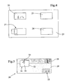
- This combination is shown schematically in figure 4 , in which, as said, element 24 could correspond to the embodiment of figure 1D , elements 25 and 26 could correspond to the embodiment of figure 2 , and element 27 could correspond to the embodiment of figure 3 , for example. Any combination would further improve the features of the note in that it would be even more difficult to copy of counterfeit since it carries different embodiments of a security element. It is also possible to combine the security elements on both sides of the substrate, using one element on one side and another (identical or different) on the other side.
- the background with at least two zones of a different color may not be printed on the substrate but could be formed by the substrate itself.
- substrate made of plastic or similar products as used for example for ID cards, credit cards and EC cards, which may easily be produced with a multicolored substrate.
- this principle may be applied to all substrate.
- a substrate 28 comprises two parts 29 and 30 of a different color, as schematically represented by a bright part 29 and a dark part 30.
- the parts 29, 30 are equivalent to the zones 1 and 2 of figure 1 .
- a security element 31 is present on the substrate 28, said element 31 comprising, as described here above, an opaque layer 32, for example a layer of optically variable ink, in which a pattern has been created by removing the layer 32 along a given path.
- the pattern has the shape of the number "1" with two colors, the upper part 33 of the color of part 30 and the lower part 34 of the color of part 29.
- the principles described above for the embodiments of figures 2 or 3 on the substrate of figure 4 may be used for this substrate. It is also possible to further combine in this embodiment the security element 31 using the different colors of the substrate itself as background with another security element in which the background of two or more colors is printed on the substrate, i.e. to apply a security element similar to the elements 24, or 25, or 26 or 27 shown in figure 4 on the substrate 28 of the embodiment of figure 5 .
- This variant is schematized by the element 35 in figure 5 corresponding schematically to the element of figure 1B , in which no specific pattern has been marked yet.
- any combination is possible, not only on the same side of the substrate, but also on both sides of the substrate.
- a process suitable for producing a security element according to the invention is shown schematically in the block diagram of figure 6 .
- the first step comprises the provision of a substrate with a first layer having at least two adjacent zones of different color.
- said two zones may be printed on the substrate or they may be formed by the substrate itself, or they may be partially printed on the substrate and partially formed by the substrate.
- the second step comprises covering at least partially said adjacent zones with a first layer that is opaque.
- staid opaque layer is engraved, preferably via a yag-laser beam, to form a pattern, for example a number, a sequence of numbers, a letter, a sequence of letters or a combination of both to make the first layer apparent.
- a pattern for example a number, a sequence of numbers, a letter, a sequence of letters or a combination of both to make the first layer apparent.
Landscapes
- Business, Economics & Management (AREA)
- Accounting & Taxation (AREA)
- Finance (AREA)
- Physics & Mathematics (AREA)
- General Physics & Mathematics (AREA)
- Engineering & Computer Science (AREA)
- Theoretical Computer Science (AREA)
- Credit Cards Or The Like (AREA)
- Printing Methods (AREA)
Claims (21)
- Un support de données, tel que des billets de banque, des titres, des chèques, des cartes de crédit, des cartes d'identité et des documents similaires, comprenant un élément de sécurité, lequel support de données comprend un substrat (23,28) avec une première couche de matériau qui est imprimée sur et/ou formée par ledit substrat (23,28) et au moins une première couche opaque (3) de matériau recouvrant partiellement ou entièrement ladite première couche de matériau, ladite première couche présentant au moins deux zones adjacentes (1,2) d'une couleur différente,
l'élément de sécurité comprenant en outre un motif (4,8) formé par une gravure partielle de ladite première couche opaque (3), ledit motif (4,8) s'étendant au moins partiellement sur chacune desdites zones (1,2) de telle sorte que ledit motif (4,8) comporte des parties adjacentes de couleur différente en registre, apparentes à travers ladite première couche opaque (3). - Un support de données selon la revendication 1, caractérisé en ce que ladite première couche est imprimée sur ledit substrat (23).
- Un support de données selon la revendication 1, caractérisé en ce que ladite première couche est formée par ledit substrat (28).
- Un support de données selon la revendication 1, caractérisé en ce que ladite première couche est partiellement formée par ledit substrat (28) et partiellement imprimée sur ledit substrat (28).
- Un support de données selon l'une quelconque des revendications précédentes, caractérisé en ce qu'il comporte une deuxième couche opaque (19) recouvrant au moins partiellement ladite première couche et ladite première couche opaque (3), ledit motif étant formé par une gravure partielle desdites première et deuxième couches opaques.
- Un support de données selon l'une quelconque des revendications précédentes, caractérisé en ce que ladite couche opaque (3) ou lesdites couches opaques (3,19) sont formées d'une encre optiquement variable ou d'un dispositif optiquement variable, ou d'une combinaison des deux.
- Un support de données selon l'une quelconque des revendications précédentes, caractérisé en ce que ledit motif (4,8) est formé en gravant ladite couche opaque (3) ou lesdites couches opaques (3,19) le long d'une forme correspondant au dit motif.
- Un support de données selon la revendication 7, ladite forme consistant en une ligne mince qui suit la périphérie du motif (8).
- Un support de données selon l'une quelconque des revendications précédentes, caractérisé en ce que ledit motif prédéterminé (4,8) forme une information variable qui varie d'un support de données à un autre.
- Un support de données selon la revendication 9, caractérisé en ce que ledit motif est corrélé avec une autre information variable sur le support de données.
- Un support de données selon la revendication 10, caractérisé en ce que ledit motif corrélé est crypté et codé.
- Un support de données selon l'une quelconque des revendications précédentes, caractérisé en ce que ledit motif est formé de caractères alphanumériques et/ou de formes géométriques.
- Un procédé pour doter un support de données comportant un substrat (23, 28) d'un élément de sécurité selon l'une quelconque des revendications 1 à 12, ledit procédé étant caractérisé par les étapes suivantes :-) doter ledit substrat d'une première couche de matériau présentant au moins deux zones adjacentes de couleur différente et une première couche opaque de matériau recouvrant au moins partiellement ladite première couche de matériau-) graver ladite première couche opaque pour former un motif, ledit motif s'étendant au moins partiellement sur chacune desdites zones de telle sorte que ledit motif comporte des parties adjacentes de couleur différente en registre, apparentes à travers ladite couche opaque.
- Un procédé selon la revendication 13, caractérisé en ce que ladite première couche est imprimée sur ledit substrat.
- Un procédé selon la revendication 13, caractérisé en ce que ladite première couche est formée par ledit substrat.
- Un procédé selon la revendication 13, caractérisé en ce que ladite première couche est partiellement formée par ledit substrat (28) et partiellement imprimée sur ledit substrat (28).
- Un procédé selon l'une quelconque des revendications 13 à 16, caractérisé en ce que ledit substrat est muni d'une deuxième couche opaque recouvrant au moins partiellement ladite première couche et ladite première couche opaque, ledit motif étant formé en gravant lesdites première et deuxième couches opaques.
- Un procédé selon l'une quelconque des revendications 13 à 17, caractérisé en ce que ladite couche opaque ou lesdites couches opaques sont formées d'une encre optiquement variable ou d'un dispositif optiquement variable, ou d'une combinaison des deux.
- Un procédé selon l'une quelconque des revendications 13 à 18, caractérisé en ce que ledit motif est formé en gravant ladite couche opaque ou lesdites couches opaques le long d'une forme correspondant au dit motif.
- Un procédé selon la revendication 19, ladite forme consistant en une ligne mince qui suit la périphérie du motif (8).
- Un procédé selon l'une quelconque des revendications 13 à 20, caractérisé en ce que ladite gravure desdites couches opaques est réalisée par un laser.
Priority Applications (1)
| Application Number | Priority Date | Filing Date | Title |
|---|---|---|---|
| EP03704897A EP1485870B1 (fr) | 2002-03-15 | 2003-03-06 | Element de securite pour un support de donnees |
Applications Claiming Priority (4)
| Application Number | Priority Date | Filing Date | Title |
|---|---|---|---|
| EP20020405203 EP1345166A1 (fr) | 2002-03-15 | 2002-03-15 | Elément de sécurité pour support de données |
| EP02405203 | 2002-03-15 | ||
| EP03704897A EP1485870B1 (fr) | 2002-03-15 | 2003-03-06 | Element de securite pour un support de donnees |
| PCT/IB2003/000831 WO2003079283A1 (fr) | 2002-03-15 | 2003-03-06 | Element de securite pour un support de donnees |
Publications (2)
| Publication Number | Publication Date |
|---|---|
| EP1485870A1 EP1485870A1 (fr) | 2004-12-15 |
| EP1485870B1 true EP1485870B1 (fr) | 2011-11-09 |
Family
ID=27763483
Family Applications (2)
| Application Number | Title | Priority Date | Filing Date |
|---|---|---|---|
| EP20020405203 Withdrawn EP1345166A1 (fr) | 2002-03-15 | 2002-03-15 | Elément de sécurité pour support de données |
| EP03704897A Revoked EP1485870B1 (fr) | 2002-03-15 | 2003-03-06 | Element de securite pour un support de donnees |
Family Applications Before (1)
| Application Number | Title | Priority Date | Filing Date |
|---|---|---|---|
| EP20020405203 Withdrawn EP1345166A1 (fr) | 2002-03-15 | 2002-03-15 | Elément de sécurité pour support de données |
Country Status (10)
| Country | Link |
|---|---|
| US (1) | US20060056652A1 (fr) |
| EP (2) | EP1345166A1 (fr) |
| JP (1) | JP2005520711A (fr) |
| KR (1) | KR20050007438A (fr) |
| CN (1) | CN1313968C (fr) |
| AT (1) | ATE533124T1 (fr) |
| AU (1) | AU2003207895A1 (fr) |
| CA (1) | CA2478472A1 (fr) |
| RU (1) | RU2308757C2 (fr) |
| WO (1) | WO2003079283A1 (fr) |
Families Citing this family (13)
| Publication number | Priority date | Publication date | Assignee | Title |
|---|---|---|---|---|
| ITMI20011889A1 (it) | 2001-09-10 | 2003-03-10 | Elmiva S A S Di Walter Mantega | Procedimento contro la falsificazione e la contraffazione di documenti di valore in particolare banconote |
| US9507930B2 (en) | 2003-04-25 | 2016-11-29 | Z124 | Physical key secure peripheral interconnection |
| EP1473152A1 (fr) | 2003-04-30 | 2004-11-03 | Kba-Giori S.A. | Dispositif pour appliqué et coupé des bandes d'aggloméré laminé |
| DE102004038542A1 (de) | 2004-08-06 | 2006-02-23 | Giesecke & Devrient Gmbh | Datenträger mit Sicherheitselement und Verfahren zu seiner Herstellung |
| DE102005025095A1 (de) | 2005-06-01 | 2006-12-07 | Giesecke & Devrient Gmbh | Datenträger und Verfahren zu seiner Herstellung |
| US20090080760A1 (en) * | 2007-09-21 | 2009-03-26 | Microsecurity Lab Inc. | Anti-counterfeiting mark and methods |
| EA200900975A1 (ru) * | 2009-06-25 | 2010-04-30 | Открытое Акционерное Общество «Научно-Производственное Объединение "Криптен"» | Оптический защитный элемент, способ его изготовления и способ верификации аутентичности объекта с указанным защитным элементом |
| DE102010063012B4 (de) * | 2010-12-14 | 2018-10-18 | Bundesdruckerei Gmbh | Aktivierbares Sicherheitselement |
| EP2511104A1 (fr) * | 2011-04-14 | 2012-10-17 | Gemalto SA | Document de sécurité et son procédé de fabrication |
| US9383770B2 (en) | 2011-08-31 | 2016-07-05 | Z124 | Mobile device that docks with multiple types of docks |
| US9244491B2 (en) | 2011-08-31 | 2016-01-26 | Z124 | Smart dock for auxiliary devices |
| CA3016788A1 (fr) * | 2018-09-07 | 2020-03-07 | Canadian Bank Note Company, Limited | Dispositifs de securite pour documents securises |
| KR102253771B1 (ko) * | 2019-11-12 | 2021-05-21 | 주식회사 진학사 | 웹페이지에서의 숫자 표기 방법 및 시스템 |
Family Cites Families (17)
| Publication number | Priority date | Publication date | Assignee | Title |
|---|---|---|---|---|
| US4816322A (en) * | 1981-11-02 | 1989-03-28 | Dennison Manufacturing Company | Anticounterfeit metallized labels |
| US4897533A (en) * | 1987-07-07 | 1990-01-30 | National Business Systems, Inc. | Credit card and method of making the same |
| JPH074955B2 (ja) * | 1987-12-22 | 1995-01-25 | 日本ビクター株式会社 | 熱転写型プリンタ |
| US5876068A (en) * | 1988-03-04 | 1999-03-02 | Gao Gessellschaft Fur Automation Und Organisation Gmbh | Security element in the form of a thread or strip to be embedded in security documents and methods of producing it |
| DE58906399D1 (de) * | 1988-05-18 | 1994-01-27 | De La Rue Giori Sa | Konvertierbare Mehrfarben-Druckmaschine zum Schön- und Widerdruck, insbesondere von Banknoten. |
| DE3840729C2 (de) * | 1988-12-02 | 1997-07-17 | Gao Ges Automation Org | Mehrschichtiger Aufzeichnungsträger und Verfahren zum Beschriften eines mehrschichtigen Aufzeichnungsträgers |
| DE4410431A1 (de) * | 1994-03-25 | 1995-09-28 | Giesecke & Devrient Gmbh | Vor unerlaubter Reproduktion mit einem Kopiergerät geschützte Ausweiskarte |
| DE4447428C2 (de) * | 1994-05-18 | 1997-09-11 | Orga Kartensysteme Gmbh | Verfahren zur Herstellung eines in eine Ausweiskarte einzubringenden Bildes |
| DE4446368A1 (de) * | 1994-12-23 | 1996-06-27 | Giesecke & Devrient Gmbh | Datenträger mit einem optisch variablen Element |
| JP2799157B2 (ja) * | 1995-06-28 | 1998-09-17 | 東芝イーエムアイ株式会社 | 複合光ディスク構造体およびその製造用金型 |
| JPH0963128A (ja) * | 1995-08-28 | 1997-03-07 | Mitsui Toatsu Chem Inc | 光記録媒体の刻印方法 |
| DE19704478A1 (de) * | 1997-02-06 | 1998-08-13 | Merck Patent Gmbh | Lasermarkierbare Papiere und Kartonagen |
| UA52804C2 (uk) * | 1997-12-02 | 2003-01-15 | Текнікал Графікс Сек'Юріті Продактс, Ллс | Магнітний/металевий захисний пристрій (варіанти), спосіб його виготовлення (варіанти), спосіб встановлення його автентичності і металевий захисний пристрій |
| JP2000177281A (ja) * | 1998-12-14 | 2000-06-27 | Toppan Printing Co Ltd | Ovd画像付き入場券 |
| FR2803939B1 (fr) * | 2000-01-18 | 2002-03-01 | Rexor | Fil de securite ou film de transfert pour marquage a chaud pour billets de banque, documents ou autres articles a securiser |
| JP4626016B2 (ja) * | 2000-06-19 | 2011-02-02 | 凸版印刷株式会社 | 偽造防止カードの作製方法 |
| JP2002067509A (ja) * | 2000-09-01 | 2002-03-08 | Dainippon Printing Co Ltd | 情報記録方法及び情報記録媒体 |
-
2002
- 2002-03-15 EP EP20020405203 patent/EP1345166A1/fr not_active Withdrawn
-
2003
- 2003-03-06 WO PCT/IB2003/000831 patent/WO2003079283A1/fr not_active Ceased
- 2003-03-06 RU RU2004130471/09A patent/RU2308757C2/ru active
- 2003-03-06 CN CNB038061503A patent/CN1313968C/zh not_active Expired - Fee Related
- 2003-03-06 AU AU2003207895A patent/AU2003207895A1/en not_active Abandoned
- 2003-03-06 US US10/507,801 patent/US20060056652A1/en not_active Abandoned
- 2003-03-06 KR KR10-2004-7014134A patent/KR20050007438A/ko not_active Ceased
- 2003-03-06 AT AT03704897T patent/ATE533124T1/de active
- 2003-03-06 CA CA002478472A patent/CA2478472A1/fr not_active Abandoned
- 2003-03-06 JP JP2003577208A patent/JP2005520711A/ja active Pending
- 2003-03-06 EP EP03704897A patent/EP1485870B1/fr not_active Revoked
Also Published As
| Publication number | Publication date |
|---|---|
| CN1643542A (zh) | 2005-07-20 |
| RU2004130471A (ru) | 2005-04-10 |
| RU2308757C2 (ru) | 2007-10-20 |
| EP1345166A1 (fr) | 2003-09-17 |
| CA2478472A1 (fr) | 2003-09-25 |
| KR20050007438A (ko) | 2005-01-18 |
| WO2003079283A1 (fr) | 2003-09-25 |
| US20060056652A1 (en) | 2006-03-16 |
| ATE533124T1 (de) | 2011-11-15 |
| EP1485870A1 (fr) | 2004-12-15 |
| JP2005520711A (ja) | 2005-07-14 |
| AU2003207895A1 (en) | 2003-09-29 |
| CN1313968C (zh) | 2007-05-02 |
Similar Documents
| Publication | Publication Date | Title |
|---|---|---|
| RU2176190C2 (ru) | Носитель информации, содержащий элемент с оптически переменными свойствами, способ изготовления такого носителя информации (варианты) и защитный элемент с оптически переменными свойствами | |
| AU2003256017B2 (en) | Reinforced substrate for securities | |
| CA2496829C (fr) | Support de donnees avec element a variabilite optique | |
| KR101121123B1 (ko) | 인쇄기 및 인쇄방법 | |
| EP2065187B1 (fr) | Procédé de production de papiers de sécurité, machine d'héliogravure pour réaliser ce procédé, et papier de sécurité produit par ce procédé | |
| CA2401071C (fr) | Procede de production de supports de donnees pouvant etre marques au laser et supports de donnees correspondants | |
| EP1485870B1 (fr) | Element de securite pour un support de donnees | |
| EA008011B1 (ru) | Защитный знак | |
| MX2008009157A (es) | Documento de seguridad. | |
| CN100430238C (zh) | 用于印刷防护单元的方法以及防护单元 | |
| US11987067B2 (en) | Multi-page personalization for a multi-page security document | |
| CN100522648C (zh) | 有价文件 | |
| RU2392125C2 (ru) | Носитель данных с полутоновым изображением | |
| CA2238743C (fr) | Support de donnees a couleur optiquement variable | |
| HK1070030A1 (zh) | 使防偽文件個體化的方法及相應的防偽文件 | |
| MXPA05014025A (en) | Printing machine | |
| HK1070030B (en) | Method for individualising security documents and corresponding security document |
Legal Events
| Date | Code | Title | Description |
|---|---|---|---|
| PUAI | Public reference made under article 153(3) epc to a published international application that has entered the european phase |
Free format text: ORIGINAL CODE: 0009012 |
|
| 17P | Request for examination filed |
Effective date: 20040827 |
|
| AK | Designated contracting states |
Kind code of ref document: A1 Designated state(s): AT BE BG CH CY CZ DE DK EE ES FI FR GB GR HU IE IT LI LU MC NL PT RO SE SI SK TR |
|
| AX | Request for extension of the european patent |
Extension state: AL LT LV MK RO |
|
| 17Q | First examination report despatched |
Effective date: 20080422 |
|
| RAP1 | Party data changed (applicant data changed or rights of an application transferred) |
Owner name: KBA-GIORI S.A. |
|
| RAP1 | Party data changed (applicant data changed or rights of an application transferred) |
Owner name: KBA-NOTASYS SA |
|
| GRAP | Despatch of communication of intention to grant a patent |
Free format text: ORIGINAL CODE: EPIDOSNIGR1 |
|
| GRAS | Grant fee paid |
Free format text: ORIGINAL CODE: EPIDOSNIGR3 |
|
| GRAA | (expected) grant |
Free format text: ORIGINAL CODE: 0009210 |
|
| AK | Designated contracting states |
Kind code of ref document: B1 Designated state(s): AT BE BG CH CY CZ DE DK EE ES FI FR GB GR HU IE IT LI LU MC NL PT RO SE SI SK TR |
|
| REG | Reference to a national code |
Ref country code: GB Ref legal event code: FG4D |
|
| REG | Reference to a national code |
Ref country code: CH Ref legal event code: EP |
|
| REG | Reference to a national code |
Ref country code: IE Ref legal event code: FG4D |
|
| REG | Reference to a national code |
Ref country code: DE Ref legal event code: R096 Ref document number: 60339056 Country of ref document: DE Effective date: 20111229 |
|
| REG | Reference to a national code |
Ref country code: NL Ref legal event code: T3 |
|
| PG25 | Lapsed in a contracting state [announced via postgrant information from national office to epo] |
Ref country code: GR Free format text: LAPSE BECAUSE OF FAILURE TO SUBMIT A TRANSLATION OF THE DESCRIPTION OR TO PAY THE FEE WITHIN THE PRESCRIBED TIME-LIMIT Effective date: 20120210 Ref country code: SE Free format text: LAPSE BECAUSE OF FAILURE TO SUBMIT A TRANSLATION OF THE DESCRIPTION OR TO PAY THE FEE WITHIN THE PRESCRIBED TIME-LIMIT Effective date: 20111109 Ref country code: BE Free format text: LAPSE BECAUSE OF FAILURE TO SUBMIT A TRANSLATION OF THE DESCRIPTION OR TO PAY THE FEE WITHIN THE PRESCRIBED TIME-LIMIT Effective date: 20111109 Ref country code: SI Free format text: LAPSE BECAUSE OF FAILURE TO SUBMIT A TRANSLATION OF THE DESCRIPTION OR TO PAY THE FEE WITHIN THE PRESCRIBED TIME-LIMIT Effective date: 20111109 Ref country code: PT Free format text: LAPSE BECAUSE OF FAILURE TO SUBMIT A TRANSLATION OF THE DESCRIPTION OR TO PAY THE FEE WITHIN THE PRESCRIBED TIME-LIMIT Effective date: 20120309 |
|
| PG25 | Lapsed in a contracting state [announced via postgrant information from national office to epo] |
Ref country code: CY Free format text: LAPSE BECAUSE OF FAILURE TO SUBMIT A TRANSLATION OF THE DESCRIPTION OR TO PAY THE FEE WITHIN THE PRESCRIBED TIME-LIMIT Effective date: 20111109 |
|
| PG25 | Lapsed in a contracting state [announced via postgrant information from national office to epo] |
Ref country code: EE Free format text: LAPSE BECAUSE OF FAILURE TO SUBMIT A TRANSLATION OF THE DESCRIPTION OR TO PAY THE FEE WITHIN THE PRESCRIBED TIME-LIMIT Effective date: 20111109 Ref country code: BG Free format text: LAPSE BECAUSE OF FAILURE TO SUBMIT A TRANSLATION OF THE DESCRIPTION OR TO PAY THE FEE WITHIN THE PRESCRIBED TIME-LIMIT Effective date: 20120209 Ref country code: DK Free format text: LAPSE BECAUSE OF FAILURE TO SUBMIT A TRANSLATION OF THE DESCRIPTION OR TO PAY THE FEE WITHIN THE PRESCRIBED TIME-LIMIT Effective date: 20111109 Ref country code: CZ Free format text: LAPSE BECAUSE OF FAILURE TO SUBMIT A TRANSLATION OF THE DESCRIPTION OR TO PAY THE FEE WITHIN THE PRESCRIBED TIME-LIMIT Effective date: 20111109 Ref country code: SK Free format text: LAPSE BECAUSE OF FAILURE TO SUBMIT A TRANSLATION OF THE DESCRIPTION OR TO PAY THE FEE WITHIN THE PRESCRIBED TIME-LIMIT Effective date: 20111109 |
|
| PLBI | Opposition filed |
Free format text: ORIGINAL CODE: 0009260 |
|
| PG25 | Lapsed in a contracting state [announced via postgrant information from national office to epo] |
Ref country code: RO Free format text: LAPSE BECAUSE OF FAILURE TO SUBMIT A TRANSLATION OF THE DESCRIPTION OR TO PAY THE FEE WITHIN THE PRESCRIBED TIME-LIMIT Effective date: 20111109 |
|
| 26 | Opposition filed |
Opponent name: GIESECKE & DEVRIENT GMBH Effective date: 20120806 |
|
| PLAX | Notice of opposition and request to file observation + time limit sent |
Free format text: ORIGINAL CODE: EPIDOSNOBS2 |
|
| REG | Reference to a national code |
Ref country code: AT Ref legal event code: MK05 Ref document number: 533124 Country of ref document: AT Kind code of ref document: T Effective date: 20111109 |
|
| PG25 | Lapsed in a contracting state [announced via postgrant information from national office to epo] |
Ref country code: MC Free format text: LAPSE BECAUSE OF NON-PAYMENT OF DUE FEES Effective date: 20120331 |
|
| REG | Reference to a national code |
Ref country code: DE Ref legal event code: R026 Ref document number: 60339056 Country of ref document: DE Effective date: 20120806 |
|
| REG | Reference to a national code |
Ref country code: IE Ref legal event code: MM4A |
|
| PLAF | Information modified related to communication of a notice of opposition and request to file observations + time limit |
Free format text: ORIGINAL CODE: EPIDOSCOBS2 |
|
| PG25 | Lapsed in a contracting state [announced via postgrant information from national office to epo] |
Ref country code: IE Free format text: LAPSE BECAUSE OF NON-PAYMENT OF DUE FEES Effective date: 20120306 Ref country code: AT Free format text: LAPSE BECAUSE OF FAILURE TO SUBMIT A TRANSLATION OF THE DESCRIPTION OR TO PAY THE FEE WITHIN THE PRESCRIBED TIME-LIMIT Effective date: 20111109 |
|
| PG25 | Lapsed in a contracting state [announced via postgrant information from national office to epo] |
Ref country code: ES Free format text: LAPSE BECAUSE OF FAILURE TO SUBMIT A TRANSLATION OF THE DESCRIPTION OR TO PAY THE FEE WITHIN THE PRESCRIBED TIME-LIMIT Effective date: 20120220 |
|
| PG25 | Lapsed in a contracting state [announced via postgrant information from national office to epo] |
Ref country code: FI Free format text: LAPSE BECAUSE OF FAILURE TO SUBMIT A TRANSLATION OF THE DESCRIPTION OR TO PAY THE FEE WITHIN THE PRESCRIBED TIME-LIMIT Effective date: 20111109 |
|
| PLBB | Reply of patent proprietor to notice(s) of opposition received |
Free format text: ORIGINAL CODE: EPIDOSNOBS3 |
|
| PG25 | Lapsed in a contracting state [announced via postgrant information from national office to epo] |
Ref country code: TR Free format text: LAPSE BECAUSE OF FAILURE TO SUBMIT A TRANSLATION OF THE DESCRIPTION OR TO PAY THE FEE WITHIN THE PRESCRIBED TIME-LIMIT Effective date: 20111109 |
|
| PG25 | Lapsed in a contracting state [announced via postgrant information from national office to epo] |
Ref country code: LU Free format text: LAPSE BECAUSE OF NON-PAYMENT OF DUE FEES Effective date: 20120306 |
|
| PG25 | Lapsed in a contracting state [announced via postgrant information from national office to epo] |
Ref country code: HU Free format text: LAPSE BECAUSE OF FAILURE TO SUBMIT A TRANSLATION OF THE DESCRIPTION OR TO PAY THE FEE WITHIN THE PRESCRIBED TIME-LIMIT Effective date: 20030306 |
|
| RDAF | Communication despatched that patent is revoked |
Free format text: ORIGINAL CODE: EPIDOSNREV1 |
|
| APBM | Appeal reference recorded |
Free format text: ORIGINAL CODE: EPIDOSNREFNO |
|
| APBP | Date of receipt of notice of appeal recorded |
Free format text: ORIGINAL CODE: EPIDOSNNOA2O |
|
| APAH | Appeal reference modified |
Free format text: ORIGINAL CODE: EPIDOSCREFNO |
|
| REG | Reference to a national code |
Ref country code: FR Ref legal event code: PLFP Year of fee payment: 14 |
|
| PLBP | Opposition withdrawn |
Free format text: ORIGINAL CODE: 0009264 |
|
| REG | Reference to a national code |
Ref country code: FR Ref legal event code: PLFP Year of fee payment: 15 |
|
| PGFP | Annual fee paid to national office [announced via postgrant information from national office to epo] |
Ref country code: NL Payment date: 20170321 Year of fee payment: 15 |
|
| REG | Reference to a national code |
Ref country code: FR Ref legal event code: PLFP Year of fee payment: 16 |
|
| REG | Reference to a national code |
Ref country code: NL Ref legal event code: MM Effective date: 20180401 |
|
| PG25 | Lapsed in a contracting state [announced via postgrant information from national office to epo] |
Ref country code: NL Free format text: LAPSE BECAUSE OF NON-PAYMENT OF DUE FEES Effective date: 20180401 |
|
| PGFP | Annual fee paid to national office [announced via postgrant information from national office to epo] |
Ref country code: CH Payment date: 20190322 Year of fee payment: 17 Ref country code: FR Payment date: 20190322 Year of fee payment: 17 Ref country code: GB Payment date: 20190322 Year of fee payment: 17 Ref country code: DE Payment date: 20190304 Year of fee payment: 17 |
|
| PGFP | Annual fee paid to national office [announced via postgrant information from national office to epo] |
Ref country code: IT Payment date: 20190329 Year of fee payment: 17 |
|
| REG | Reference to a national code |
Ref country code: DE Ref legal event code: R119 Ref document number: 60339056 Country of ref document: DE |
|
| REG | Reference to a national code |
Ref country code: CH Ref legal event code: PL |
|
| REG | Reference to a national code |
Ref country code: DE Ref legal event code: R064 Ref document number: 60339056 Country of ref document: DE Ref country code: DE Ref legal event code: R103 Ref document number: 60339056 Country of ref document: DE |
|
| APBU | Appeal procedure closed |
Free format text: ORIGINAL CODE: EPIDOSNNOA9O |
|
| RDAG | Patent revoked |
Free format text: ORIGINAL CODE: 0009271 |
|
| STAA | Information on the status of an ep patent application or granted ep patent |
Free format text: STATUS: PATENT REVOKED |
|
| REG | Reference to a national code |
Ref country code: FI Ref legal event code: MGE |
|
| 27W | Patent revoked |
Effective date: 20201208 |
|
| GBPR | Gb: patent revoked under art. 102 of the ep convention designating the uk as contracting state |
Effective date: 20201208 |
|
| PG25 | Lapsed in a contracting state [announced via postgrant information from national office to epo] |
Ref country code: DE Free format text: LAPSE BECAUSE OF NON-PAYMENT OF DUE FEES Effective date: 20201001 Ref country code: CH Free format text: LAPSE BECAUSE OF NON-PAYMENT OF DUE FEES Effective date: 20200331 Ref country code: LI Free format text: LAPSE BECAUSE OF NON-PAYMENT OF DUE FEES Effective date: 20200331 Ref country code: FR Free format text: LAPSE BECAUSE OF NON-PAYMENT OF DUE FEES Effective date: 20200331 |
|
| PG25 | Lapsed in a contracting state [announced via postgrant information from national office to epo] |
Ref country code: IT Free format text: LAPSE BECAUSE OF NON-PAYMENT OF DUE FEES Effective date: 20200306 |
|
| PG25 | Lapsed in a contracting state [announced via postgrant information from national office to epo] |
Ref country code: GB Free format text: LAPSE BECAUSE OF NON-PAYMENT OF DUE FEES Effective date: 20200603 |