EP1487009A1 - Cassette de stockage de multiples feuilles de plaquettes semi-conductrices - Google Patents
Cassette de stockage de multiples feuilles de plaquettes semi-conductrices Download PDFInfo
- Publication number
- EP1487009A1 EP1487009A1 EP02788655A EP02788655A EP1487009A1 EP 1487009 A1 EP1487009 A1 EP 1487009A1 EP 02788655 A EP02788655 A EP 02788655A EP 02788655 A EP02788655 A EP 02788655A EP 1487009 A1 EP1487009 A1 EP 1487009A1
- Authority
- EP
- European Patent Office
- Prior art keywords
- cassette
- semiconductor wafer
- adsorber
- plates
- vertical direction
- Prior art date
- Legal status (The legal status is an assumption and is not a legal conclusion. Google has not performed a legal analysis and makes no representation as to the accuracy of the status listed.)
- Granted
Links
Images



Classifications
-
- H—ELECTRICITY
- H10—SEMICONDUCTOR DEVICES; ELECTRIC SOLID-STATE DEVICES NOT OTHERWISE PROVIDED FOR
- H10P—GENERIC PROCESSES OR APPARATUS FOR THE MANUFACTURE OR TREATMENT OF DEVICES COVERED BY CLASS H10
- H10P72/00—Handling or holding of wafers, substrates or devices during manufacture or treatment thereof
- H10P72/70—Handling or holding of wafers, substrates or devices during manufacture or treatment thereof for supporting or gripping
- H10P72/78—Handling or holding of wafers, substrates or devices during manufacture or treatment thereof for supporting or gripping using vacuum or suction, e.g. Bernoulli chucks
-
- H—ELECTRICITY
- H10—SEMICONDUCTOR DEVICES; ELECTRIC SOLID-STATE DEVICES NOT OTHERWISE PROVIDED FOR
- H10P—GENERIC PROCESSES OR APPARATUS FOR THE MANUFACTURE OR TREATMENT OF DEVICES COVERED BY CLASS H10
- H10P72/00—Handling or holding of wafers, substrates or devices during manufacture or treatment thereof
- H10P72/10—Handling or holding of wafers, substrates or devices during manufacture or treatment thereof using carriers specially adapted therefor, e.g. front opening unified pods [FOUP]
- H10P72/12—Vertical boat type carrier whereby the substrates are horizontally supported, e.g. comprising rod-shaped elements
- H10P72/127—Vertical boat type carrier whereby the substrates are horizontally supported, e.g. comprising rod-shaped elements characterised by the substrate support
-
- H—ELECTRICITY
- H10—SEMICONDUCTOR DEVICES; ELECTRIC SOLID-STATE DEVICES NOT OTHERWISE PROVIDED FOR
- H10P—GENERIC PROCESSES OR APPARATUS FOR THE MANUFACTURE OR TREATMENT OF DEVICES COVERED BY CLASS H10
- H10P72/00—Handling or holding of wafers, substrates or devices during manufacture or treatment thereof
- H10P72/10—Handling or holding of wafers, substrates or devices during manufacture or treatment thereof using carriers specially adapted therefor, e.g. front opening unified pods [FOUP]
- H10P72/14—Vertical carrier comprising wall type elements whereby the substrates are horizontally supported, e.g. comprising sidewalls
Definitions
- the present invention relates to a cassette for storing a plurality of semiconductor wafers with a space therebetween in the vertical direction.
- a plurality of semiconductor wafers are stored in a cassette, and the cassette is carried to a predetermined site.
- the cassette has a pair of side walls extending vertically at an interval therebetween in the crosswise direction, and in the inner sides of the side walls, support ribs or support grooves are formed with a space therebetween in the vertical direction.
- the semiconductor wafers are each stored in the cassette by positioning their both edge portions on the respective support ribs or in the respective support grooves of both the side walls. Therefore, a plurality of semiconductor wafers are stored with a space therebetween in the vertical direction (the space corresponds to an interval between adjacent support ribs or support grooves) in the cassette.
- An adsorber having suction holes in its top surface is used to carry semiconductor wafers into the cassette or to carry them out from it.
- the semiconductor wafer is vacuum adsorbed to the adsorber and carried to a predetermined position in the cassette, the vacuum adsorption of the semiconductor wafer is then released to leave the semiconductor wafer in the cassette, and the adsorber is pulled out from the cassette.
- the adsorber is put into the cassette, positioned under the semiconductor wafer to vacuum adsorb the semiconductor wafer, and then, the adsorber suction-holding the semiconductor wafer is pulled out from the cassette.
- each semiconductor wafer is often made extremely small, for example, to 100 ⁇ m or less, particularly 50 ⁇ m or less, in recent years.
- a semiconductor wafer having an extremely small thickness is stored in the cassette, it may be bent in a concave form so that its center portion is liable to be displaced in a downward direction. Since the curvature of each semiconductor wafer is not always the same, when the semiconductor wafer bends, the space in the vertical direction between adjacent semiconductor wafers stored in the cassette with a space therebetween in the vertical direction becomes extremely small locally.
- the adsorber when the adsorber is inserted into the cassette and positioned under the semiconductor wafer, it may bump into the semiconductor wafer and damage the semiconductor wafer. Further, there is a possibility that when the semiconductor wafer greatly bends, it may come into contact with another semiconductor wafer arranged adjacent thereto in the vertical direction, whereby the semiconductor wafer may be damaged.
- JP-A 2000-91400 discloses a cassette provided with a plurality of support plates arranged with a space therebetween in the vertical direction to define a plurality of semiconductor wafer storage spaces in the cassette.
- Each of the support plates has a cut-out correspondent to the shape of an adsorber for suction-holding a semiconductor wafer.
- each semiconductor wafer is supported not only at its both edge portions but also at its center portion, thereby suppressing its curvature caused by its own weight. As semiconductor wafers adjacent to each other in the vertical direction are separated from each other by the support plate, they are not contacted to each other.
- the cassette disclosed by the above JP-A 2000-91400 remains yet not satisfactory. According to the experience of the inventor of the present invention, a semiconductor wafer which has been made very thin by grinding its back surface is bent in a concave or convex form due to grinding distortion or crystal orientation. Therefore, even when the semiconductor wafer is supported at its both edge portions and its center portion, the semiconductor wafer is curved. Accordingly, even when the cassette disclosed by JP-A 2000-91400 is used, there still exists a possibility that the adsorber may bump into the semiconductor wafer and damage it, at the time when the adsorber is inserted into the cassette.
- a plurality of support plates are provided spaced apart from one another in the vertical direction and further, separation plates are provided between adjacent support plates.
- a cassette for storing a plurality of semiconductor wafers with a space therebetween in the vertical direction comprising a plurality of support plates which are provided spaced apart from one another in the vertical direction and have a receiving cut-out correspondent to the shape of an adsorber for suction-holding a semiconductor wafer in the front half portions of the surface plates, wherein separation plates are provided between adjacent support plates.
- the separation plates are plates having a shape correspondent to the shape of the semiconductor wafer.
- the cassette comprises a top plate above the uppermost support plate and a bottom plate under the lowest positional support plate.
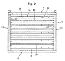
- a cassette denoted by reference numeral 2 as a whole and constituted according to the present invention comprises a top plate 4 and a bottom plate 6.
- the top plate 4 has a substantially disk-like shape and an arcuate projection portion 8 at both sides.
- the bottom plate 6 also has a substantially disk-like shape and an arcuate projection portion 10 at both sides.
- Side walls 12 extending vertically are fixed between the projection portions 8 of the top plate 4 and the projection portions 10 of the bottom plate 6.
- a pair of rear members 14 extending vertically are secured to the rear ends of the top plate 4 and the bottom plate 6 at an interval therebetween.
- Grip members 16 having a channel-like cross section are fixed on the respective projection portions 8 of the top plate 4. To carry the cassette 2 manually or by a proper carrying means (not shown), the grip portions 16 may be held.
- a plurality of (5 plates in the illustrated embodiment) of support plates 18 are provided, with a predetermined space therebetween in the vertical direction, between the top plate 4 and the bottom plate 6. Separation plates 20 are provided between each of adjacent support plates 18.
- a plurality of (9 pieces in the illustrated embodiment) of support ribs 22 are formed on the inner sides of the side walls 12 with a predetermined space therebetween in the vertical direction.
- a plurality of (9 pieces in the illustrated embodiment) of support ribs 24 are formed on the inner sides of the rear members 14 with a predetermined space therebetween in the vertical direction.
- each of the support plates 18 is substantially semicircular, its both side portions are made linear along the inner surfaces of the side walls 12, and a receiving cut-out 26 correspondent to the shape of an adsorber to be described later are formed in its front half portion.
- each of the separation plates 20 has a substantially disk-like shape correspondent to the shape of the semiconductor wafer, and its both side portions are made linear along the inner surfaces of the side walls 12.
- the cassette 2 as described above can be manufactured favorably by forming its constituent elements (that is, the top plate 3, bottom plate 6, side walls 12, rear members 14, grip members 16, support plates 18 and separation plates 20) from a synthetic resin or metal sheet and joining them together by a suitable means such as an adhesive.
- Fig. 6 shows a typical example of a semiconductor wafer carrying means 28 used to carry a semiconductor wafer into, and out from, the cassette 2.
- the illustrated semiconductor wafer carrying means 28 which is known per se comprises a lift shaft 32 mounted on a base 30 so as to be able to ascend and descend, a first swing arm 34 rotatably mounted on the top end of the lift shaft 32, a second swing arm 36 rotatably mounted on the end of the first swing arm 34, a mounting block 38 secured to the end of the second swing arm 36, and an adsorber 42 turnably mounted to the mounting block 38 on a central axis 40 extending substantially horizontally as the center.
- the illustrated adsorber 42 has a bifurcate fork-like form, and porous suction pieces 46 are formed in the respective suction surfaces (top surfaces in Fig. 6) of two fingers 44.
- Another suitable adsorber may be used as desired, and it is important that the shape of the receiving cut-out 26 in the support plate 18 should correspond to the shape of the adsorber in use.
- the semiconductor wafer carrying means 28 is provided with a lifting means (not shown) for vertically moving the lift shaft 32, the first swinging means (not shown) for swinging the first swing arm 34, the second swinging means (not shown) for swinging the second swing arm 36 and a rotary means (not shown) for rotating the adsorber 42. Further, it is further provided with a suction means for communicating the suction pieces 46 of the adsorber 42 with a vacuum source selectively.
- the semiconductor wafer 48 has a substantially disk-like shape and a linear edge 50 called "orientation flat" at part of its periphery.
- the suction surface of the adsorber 42 is brought into a close contacted with one side of the semiconductor wafer 48 to communicate the suction pieces 46 with the vacuum source, thereby causing the adsorber 42 to adsorb the semiconductor wafer 48.
- the adsorber 42 of the semiconductor wafer carrying means 28 is rotated at 180° from the state shown in Fig. 6 to direct the suction surface having the suction pieces 46 downward.
- the suction surface of the adsorber 42 is pressed against the faced-up back side of the semiconductor wafer 48 on the chuck means to adsorb the semiconductor wafer 48 thereto.
- Figs. 7 show an example of how to carry the semiconductor wafer 48 that has been adsorbed to the adsorber 42, onto the support plate 18 locating at the uppermost top position of the cassette 2.
- the adsorber 42 is rotated at 180° to direct the suction surface adsorbing the semiconductor wafer 48 upward.
- the adsorber 42 and the semiconductor wafer 48 adsorbed to the suction surface thereof are inserted into the cassette 2 by aligning the two fingers 44 of the adsorber 42 with the respective receiving cut-out 26 of the support plate 18 and positioning the semiconductor wafer 48 above the support plate 18.
- the suction pieces 46 of the adsorber 42 are disconnected from the vacuum source and opened to the air to stop the adsorption of the semiconductor wafer 48.
- the adsorber 42 is lowered.
- the adsorber 42 is lowered up to the position shown in Fig. 7(B)
- the semiconductor wafer 48 is placed on the support plate 18.
- the adsorber 42 is further lowered a bit to separate the semiconductor wafer 48 placed on the support plate 18 therefrom completely. Thereafter, the adsorber 42 is pulled out from the cassette 2.
- the semiconductor wafer 48 can be carried onto support plates 18 other than the uppermost top support plate 18 in the same manner as above.
- Figs. 8 show an example of how to carry the semiconductor wafer 48 placed on the uppermost top support plate 18 out from the cassette 2.
- the adsorber 42 is inserted, in a state of its suction surface face up being maintained, between the uppermost support plate 18 and the separation plate 20 positioned under the support plate 18.
- the adsorber 42 is moved up through the receiving cut-out 26 of the support plate 18.
- the semiconductor wafer 48 is pressed against the inner side of the top plate 4 (in the case of a semiconductor wafer 48 positioned under the support plate 18, it is pressed against the inner side of the separation plate 20 positioned above the support plate 18), whereby the curvature of the semiconductor wafer 48 is corrected to make the semiconductor wafer 48 into a flattened state.
- the suction pieces 46 of the adsorber 42 are communicated with the vacuum source to adsorb the semiconductor wafer 48 to the suction surface.
- the adsorber 42 is slightly lowered to separate the semiconductor wafer 48 from the inner side of the top plate 4 (or the separation plate 20) and pulled out from the cassette 2 while adsorbing the semiconductor wafer 48.
- the adsorber 42 adsorbing the semiconductor wafer 48 is inserted into the cassette 2 in a state of its suction surface face up to place the semiconductor wafer 48 on the support plate 18 of the cassette 2, and when the semiconductor wafer 48 on the support plate 18 is carried out from the support plate 18, too, the adsorber 42 is inserted into the cassette 2 in a state of its suction surface face up.
- the adsorber 2 adsorbing the semiconductor wafer 48 may be inserted into the cassette 2 in a state of its suction surface face down, that is, in a state of the semiconductor wafer 48 being adsorbed to the under side of the adsorber 42, and placed on the separation plate 20 positioned under the support plate 18 and not on the support plate 18.
- the adsorber 42 may be inserted into the cassette 2 in a state of its suction surface face down.
Landscapes
- Container, Conveyance, Adherence, Positioning, Of Wafer (AREA)
Applications Claiming Priority (1)
| Application Number | Priority Date | Filing Date | Title |
|---|---|---|---|
| PCT/JP2002/012313 WO2004049430A1 (fr) | 2002-11-26 | 2002-11-26 | Cassette de stockage de multiples feuilles de plaquettes semi-conductrices |
Publications (3)
| Publication Number | Publication Date |
|---|---|
| EP1487009A1 true EP1487009A1 (fr) | 2004-12-15 |
| EP1487009A4 EP1487009A4 (fr) | 2007-04-11 |
| EP1487009B1 EP1487009B1 (fr) | 2008-05-07 |
Family
ID=32375604
Family Applications (1)
| Application Number | Title | Priority Date | Filing Date |
|---|---|---|---|
| EP02788655A Expired - Lifetime EP1487009B1 (fr) | 2002-11-26 | 2002-11-26 | Cassette de stockage de multiples feuilles de plaquettes semi-conductrices |
Country Status (6)
| Country | Link |
|---|---|
| US (1) | US7325692B2 (fr) |
| EP (1) | EP1487009B1 (fr) |
| CN (1) | CN1316583C (fr) |
| AU (1) | AU2002355034A1 (fr) |
| DE (1) | DE60226512D1 (fr) |
| WO (1) | WO2004049430A1 (fr) |
Cited By (1)
| Publication number | Priority date | Publication date | Assignee | Title |
|---|---|---|---|---|
| CN107887297A (zh) * | 2016-09-29 | 2018-04-06 | 株式会社斯库林集团 | 基板对齐装置及方法、基板处理装置及方法、基板排列装置及方法 |
Families Citing this family (16)
| Publication number | Priority date | Publication date | Assignee | Title |
|---|---|---|---|---|
| US7325692B2 (en) | 2002-11-26 | 2008-02-05 | Disco Corporation | Cassette having separation plates for storing a plurality of semiconductor wafers |
| JP4509713B2 (ja) * | 2004-09-13 | 2010-07-21 | 大日商事株式会社 | ウエハキャリア |
| JP4523513B2 (ja) * | 2005-08-05 | 2010-08-11 | 東京エレクトロン株式会社 | 基板受け渡し装置、基板受け渡し方法及び記憶媒体 |
| JP4973501B2 (ja) * | 2005-12-06 | 2012-07-11 | 富士通セミコンダクター株式会社 | 半導体ウェハの収納ケース及び半導体ウェハの収納方法 |
| KR20150110207A (ko) * | 2014-03-24 | 2015-10-02 | 주식회사 테라세미콘 | 보트 |
| JP6617433B2 (ja) * | 2015-04-17 | 2019-12-11 | 日本電気硝子株式会社 | ガラス基板梱包体 |
| CN108615692B (zh) * | 2016-12-12 | 2021-04-09 | 北京北方华创微电子装备有限公司 | 片盒、反应腔室和半导体设备 |
| JP6846993B2 (ja) * | 2017-06-19 | 2021-03-24 | 東京エレクトロン株式会社 | 基板保持具及びこれを用いた基板処理装置 |
| JP1624353S (fr) * | 2018-07-19 | 2019-02-12 | ||
| JP7357453B2 (ja) * | 2019-03-07 | 2023-10-06 | 東京エレクトロン株式会社 | 基板処理システムおよび基板の搬送方法 |
| CN112477092B (zh) * | 2019-09-12 | 2022-10-14 | 福州康派克光电科技有限公司 | 真空自吸附盒成型装置及成型方法 |
| US20220148899A1 (en) * | 2020-11-06 | 2022-05-12 | Changxin Memory Technologies, Inc. | Wafer boat structure, as well as wafer boat assembly and diffusion furnace with same |
| JP1700781S (ja) * | 2021-03-22 | 2021-11-29 | 基板処理装置用断熱板 | |
| JP1760960S (fr) * | 2023-06-12 | 2024-01-10 | ||
| EP4498411A3 (fr) * | 2023-06-28 | 2025-03-26 | ASM IP Holding B.V. | Système de nacelle à plaquettes, anneau de support et utilisation associée |
| TWI911672B (zh) * | 2024-03-13 | 2026-01-11 | 力晶積成電子製造股份有限公司 | 晶圓承載裝置 |
Family Cites Families (15)
| Publication number | Priority date | Publication date | Assignee | Title |
|---|---|---|---|---|
| JPS63178541A (ja) | 1987-01-20 | 1988-07-22 | Nec Corp | ウエ−ハ収納箱 |
| JPS63195736U (fr) * | 1987-06-05 | 1988-12-16 | ||
| JPH06103720B2 (ja) * | 1989-10-09 | 1994-12-14 | 株式会社東芝 | 半導体ウェハ支持キャリア |
| DE4024973C2 (de) | 1990-08-07 | 1994-11-03 | Ibm | Anordnung zum Lagern, Transportieren und Einschleusen von Substraten |
| JPH05102056A (ja) * | 1991-10-11 | 1993-04-23 | Rohm Co Ltd | ウエハー支持具 |
| US5346518A (en) * | 1993-03-23 | 1994-09-13 | International Business Machines Corporation | Vapor drain system |
| JP3233726B2 (ja) | 1993-03-30 | 2001-11-26 | 川崎製鉄株式会社 | 熱処理生産性ならびに繰り返し応力負荷によるミクロ組織変化の遅延特性に優れた軸受鋼 |
| US6156121A (en) * | 1996-12-19 | 2000-12-05 | Tokyo Electron Limited | Wafer boat and film formation method |
| JP3494554B2 (ja) * | 1997-06-26 | 2004-02-09 | 東芝セラミックス株式会社 | 半導体用治具およびその製造方法 |
| JP2937194B1 (ja) | 1998-07-15 | 1999-08-23 | 日本電気株式会社 | 基板加熱装置 |
| JP2000091400A (ja) | 1998-09-08 | 2000-03-31 | Disco Abrasive Syst Ltd | ウェーハ収容カセット |
| US6310328B1 (en) * | 1998-12-10 | 2001-10-30 | Mattson Technologies, Inc. | Rapid thermal processing chamber for processing multiple wafers |
| WO2001001828A1 (fr) | 1999-07-02 | 2001-01-11 | Spi/Semicon | Recipient de plaquette |
| EP1091391A1 (fr) | 1999-10-05 | 2001-04-11 | SICO Produktions- und Handelsges.m.b.H. | Dispositif de support pour plaquettes semiconductrices |
| US7325692B2 (en) | 2002-11-26 | 2008-02-05 | Disco Corporation | Cassette having separation plates for storing a plurality of semiconductor wafers |
-
2002
- 2002-11-26 US US10/469,047 patent/US7325692B2/en not_active Expired - Lifetime
- 2002-11-26 CN CNB028275454A patent/CN1316583C/zh not_active Expired - Lifetime
- 2002-11-26 DE DE60226512T patent/DE60226512D1/de not_active Expired - Lifetime
- 2002-11-26 WO PCT/JP2002/012313 patent/WO2004049430A1/fr not_active Ceased
- 2002-11-26 AU AU2002355034A patent/AU2002355034A1/en not_active Abandoned
- 2002-11-26 EP EP02788655A patent/EP1487009B1/fr not_active Expired - Lifetime
Cited By (2)
| Publication number | Priority date | Publication date | Assignee | Title |
|---|---|---|---|---|
| CN107887297A (zh) * | 2016-09-29 | 2018-04-06 | 株式会社斯库林集团 | 基板对齐装置及方法、基板处理装置及方法、基板排列装置及方法 |
| CN107887297B (zh) * | 2016-09-29 | 2021-08-10 | 株式会社斯库林集团 | 基板对齐装置及方法、基板处理装置及方法、基板排列装置及方法 |
Also Published As
| Publication number | Publication date |
|---|---|
| EP1487009B1 (fr) | 2008-05-07 |
| AU2002355034A1 (en) | 2004-06-18 |
| US7325692B2 (en) | 2008-02-05 |
| DE60226512D1 (de) | 2008-06-19 |
| WO2004049430A1 (fr) | 2004-06-10 |
| CN1316583C (zh) | 2007-05-16 |
| US20040256284A1 (en) | 2004-12-23 |
| CN1618125A (zh) | 2005-05-18 |
| EP1487009A4 (fr) | 2007-04-11 |
Similar Documents
| Publication | Publication Date | Title |
|---|---|---|
| US7325692B2 (en) | Cassette having separation plates for storing a plurality of semiconductor wafers | |
| US6652216B1 (en) | Method and device for changing a semiconductor wafer position | |
| US7661921B2 (en) | Semiconductor material handling system | |
| TWI822993B (zh) | 基板貼合裝置及基板貼合方法 | |
| JPH09205128A (ja) | 半導体ウェハ移送ロボット用アーム | |
| JP4841412B2 (ja) | 基板貼合せ装置 | |
| JP2000503478A (ja) | 二重基板ホルダを有する基板搬送装置 | |
| TWI672763B (zh) | 晶圓取放件以及晶圓取放件與晶圓匣之總成 | |
| KR20060060569A (ko) | 기판 반송 장치 | |
| JPH09325105A (ja) | 顕微鏡標本のカバーガラス取出し及び取付け方法 | |
| KR100904888B1 (ko) | 여러 장의 반도체 웨이퍼를 수용하기 위한 카셋트 | |
| TW200832568A (en) | Pickup device for semiconductor chip | |
| JP3937979B2 (ja) | 吸着ハンド | |
| JP5539019B2 (ja) | 基板支持装置及び真空処理装置 | |
| CN117936450A (zh) | 一种夹持翻面装置及方法 | |
| JP4319310B2 (ja) | シート吸着装置及び吸着方法 | |
| JP5373008B2 (ja) | 基板貼合せ方法 | |
| JP2006190817A (ja) | 基板移送装置及び基板移送方法 | |
| CN220382156U (zh) | 卷芯转移装置及电池加工设备 | |
| JP2003110014A (ja) | ウェーハカセット並びに半導体ウェーハの搬入方法及び搬出方法 | |
| CN222096163U (zh) | 涂胶抓手、涂胶抓手与托盘套件以及机器人 | |
| JP3904647B2 (ja) | 基板支持装置及びこの基板支持装置に基板を着脱する基板着脱装置並びに基板着脱方法 | |
| EP4340087A1 (fr) | Dispositif de levage et dispositif de transport de feuille d'électrode l'utilisant | |
| JPH07176595A (ja) | 基板搬送装置 | |
| JP2006032687A (ja) | 被加工物搬送装置 |
Legal Events
| Date | Code | Title | Description |
|---|---|---|---|
| PUAI | Public reference made under article 153(3) epc to a published international application that has entered the european phase |
Free format text: ORIGINAL CODE: 0009012 |
|
| 17P | Request for examination filed |
Effective date: 20030707 |
|
| AK | Designated contracting states |
Kind code of ref document: A1 Designated state(s): AT BE BG CH CY CZ DE DK EE ES FI FR GB GR IE IT LI LU MC NL PT SE SK TR |
|
| AX | Request for extension of the european patent |
Extension state: AL LT LV MK RO SI |
|
| DAX | Request for extension of the european patent (deleted) | ||
| RBV | Designated contracting states (corrected) |
Designated state(s): DE FR |
|
| RAP1 | Party data changed (applicant data changed or rights of an application transferred) |
Owner name: DISCO CORPORATION |
|
| A4 | Supplementary search report drawn up and despatched |
Effective date: 20070314 |
|
| RIC1 | Information provided on ipc code assigned before grant |
Ipc: H01L 21/68 20060101AFI20040614BHEP |
|
| 17Q | First examination report despatched |
Effective date: 20070713 |
|
| GRAP | Despatch of communication of intention to grant a patent |
Free format text: ORIGINAL CODE: EPIDOSNIGR1 |
|
| RIN1 | Information on inventor provided before grant (corrected) |
Inventor name: NANJO, MASATOSHI |
|
| GRAS | Grant fee paid |
Free format text: ORIGINAL CODE: EPIDOSNIGR3 |
|
| GRAA | (expected) grant |
Free format text: ORIGINAL CODE: 0009210 |
|
| AK | Designated contracting states |
Kind code of ref document: B1 Designated state(s): DE FR |
|
| REF | Corresponds to: |
Ref document number: 60226512 Country of ref document: DE Date of ref document: 20080619 Kind code of ref document: P |
|
| PLBE | No opposition filed within time limit |
Free format text: ORIGINAL CODE: 0009261 |
|
| STAA | Information on the status of an ep patent application or granted ep patent |
Free format text: STATUS: NO OPPOSITION FILED WITHIN TIME LIMIT |
|
| 26N | No opposition filed |
Effective date: 20090210 |
|
| REG | Reference to a national code |
Ref country code: FR Ref legal event code: PLFP Year of fee payment: 14 |
|
| REG | Reference to a national code |
Ref country code: FR Ref legal event code: PLFP Year of fee payment: 15 |
|
| REG | Reference to a national code |
Ref country code: FR Ref legal event code: PLFP Year of fee payment: 16 |
|
| REG | Reference to a national code |
Ref country code: FR Ref legal event code: PLFP Year of fee payment: 17 |
|
| PGFP | Annual fee paid to national office [announced via postgrant information from national office to epo] |
Ref country code: FR Payment date: 20211109 Year of fee payment: 20 Ref country code: DE Payment date: 20211005 Year of fee payment: 20 |
|
| REG | Reference to a national code |
Ref country code: DE Ref legal event code: R071 Ref document number: 60226512 Country of ref document: DE |