EP1487242A2 - Elektrische Schaltung für eine direkt modulierte Halbleiterstrahlungsquelle - Google Patents
Elektrische Schaltung für eine direkt modulierte Halbleiterstrahlungsquelle Download PDFInfo
- Publication number
- EP1487242A2 EP1487242A2 EP04090160A EP04090160A EP1487242A2 EP 1487242 A2 EP1487242 A2 EP 1487242A2 EP 04090160 A EP04090160 A EP 04090160A EP 04090160 A EP04090160 A EP 04090160A EP 1487242 A2 EP1487242 A2 EP 1487242A2
- Authority
- EP
- European Patent Office
- Prior art keywords
- radiation source
- circuit
- voltage
- semiconductor radiation
- peaking
- Prior art date
- Legal status (The legal status is an assumption and is not a legal conclusion. Google has not performed a legal analysis and makes no representation as to the accuracy of the status listed.)
- Withdrawn
Links
Images


Classifications
-
- H—ELECTRICITY
- H01—ELECTRIC ELEMENTS
- H01S—DEVICES USING THE PROCESS OF LIGHT AMPLIFICATION BY STIMULATED EMISSION OF RADIATION [LASER] TO AMPLIFY OR GENERATE LIGHT; DEVICES USING STIMULATED EMISSION OF ELECTROMAGNETIC RADIATION IN WAVE RANGES OTHER THAN OPTICAL
- H01S5/00—Semiconductor lasers
- H01S5/04—Processes or apparatus for excitation, e.g. pumping, e.g. by electron beams
- H01S5/042—Electrical excitation ; Circuits therefor
-
- H—ELECTRICITY
- H04—ELECTRIC COMMUNICATION TECHNIQUE
- H04B—TRANSMISSION
- H04B10/00—Transmission systems employing electromagnetic waves other than radio-waves, e.g. infrared, visible or ultraviolet light, or employing corpuscular radiation, e.g. quantum communication
- H04B10/50—Transmitters
- H04B10/501—Structural aspects
- H04B10/503—Laser transmitters
- H04B10/504—Laser transmitters using direct modulation
-
- H—ELECTRICITY
- H05—ELECTRIC TECHNIQUES NOT OTHERWISE PROVIDED FOR
- H05B—ELECTRIC HEATING; ELECTRIC LIGHT SOURCES NOT OTHERWISE PROVIDED FOR; CIRCUIT ARRANGEMENTS FOR ELECTRIC LIGHT SOURCES, IN GENERAL
- H05B45/00—Circuit arrangements for operating light-emitting diodes [LED]
- H05B45/10—Controlling the intensity of the light
-
- H—ELECTRICITY
- H01—ELECTRIC ELEMENTS
- H01S—DEVICES USING THE PROCESS OF LIGHT AMPLIFICATION BY STIMULATED EMISSION OF RADIATION [LASER] TO AMPLIFY OR GENERATE LIGHT; DEVICES USING STIMULATED EMISSION OF ELECTROMAGNETIC RADIATION IN WAVE RANGES OTHER THAN OPTICAL
- H01S5/00—Semiconductor lasers
- H01S5/04—Processes or apparatus for excitation, e.g. pumping, e.g. by electron beams
- H01S5/042—Electrical excitation ; Circuits therefor
- H01S5/0427—Electrical excitation ; Circuits therefor for applying modulation to the laser
Definitions
- the invention relates to an electrical circuit for a directly modulated semiconductor radiation source according to the Preamble of claim 1.
- From DE 100 65 838 A1 is an electronic Driver circuit for directly modulated semiconductor lasers known. It describes how a constant signal, through which information is to be transported so-called peaking is superimposed. This peaking influences the rising and / or falling edges the current through the semiconductor laser. The peaking is through a driver circuit causes and causes the current through the semiconductor laser and thus the light emission can be switched on and off more quickly. this makes possible the transmission of a high data rate by the Semiconductor lasers.
- FIG. 5 taken from DE 100 65 838 A1, illustrates the peaking:
- FIG. 5 shows schematically how a voltage V pk is superimposed on the constant signal of the data transmission V Dat . These two give the current I VCSEL flowing through the VCSEL laser.
- the voltage pulses V Dat and V pk and the current pulses I VCSEL are plotted against time t.
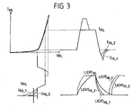
- FIG. 3 schematically shows the light radiation LICHT HL from a laser diode as a function of the current flow I HL through the laser.
- the solid line in diagram I HL relates to a data signal not modulated by peaking, the dashed lines 1 and 2 indicate the behavior of the current through the laser if the signal is modulated by peaking of different strengths.
- FIG. 3 it can be seen that the switching on and off of the light radiation LICHT HL becomes steeper due to the peaking, the laser light can be switched on and off faster.
- a disadvantage of the previously known circuit is that the peaking provides a negative current pulse through the forward voltage through the semiconductor radiation source so is greatly reduced that the next time the Semiconductor radiation source (i.e. the next positive Current pulse) Switch-on delays can occur.
- the Switch-on delays depend on the lowering of the Forward voltage at the semiconductor radiation source from and correspond to the discharge of the diffusion capacity.
- a exact coordination of the negative current pulse to be used to improve the shutdown edge proves to be technically not practicable, because in the components of the Circuit certain scatter of electrical and optical Properties prevail.
- the invention has for its object an electrical Circuit for a directly modulated Semiconductor radiation source to provide a high data transmission speed through a Can provide semiconductor radiation source.
- adverse effects are to be avoided by a Peaking the falling signal edge of a modulated current can arise from the semiconductor laser diode.
- the electrical circuit has one Semiconductor radiation source, which is dependent on one a modulated current is supplied to the digital data signal. Its falling signal edges show a peaking.
- Circuit means with an electrical contact point of the Circuit are connected, is below a predetermined value of the forward voltage at the Semiconductor radiation source the peaking of the falling Signal edge reduced or prevented. In particular, at Falling below the specified value of the forward voltage Do not further discharge semiconductor radiation source or a further reduction of the forward voltage prevented.
- the circuit means preferably form one type "Clamping circuit" that the existing circuit on the electrical contact point is switched on, or a Entladepuls horrung.
- the circuit means are preferably characterized in that they contribute the current through the semiconductor radiation source Falling below the specified value of the forward voltage at least partially divert or switch off.
- the current through the semiconductor radiation source is thereby deflected and flows through the clamp circuit.
- the circuit means preferably have at least one Transistor on, which is blocked as long as the on Semiconductor radiation source applied voltage above the considered given value of the forward voltage at the Semiconductor radiation source.
- the transistor will conductive once the voltage reaches the specified limit reached. This can happen, for example, in that such a transistor, for example a PNP or an NPN transistor is based on a DC voltage source lies and its emitter with the electrical contact point is connected to the semiconductor radiation source. Dependent on from that provided by the DC voltage source The voltage will exceed the certain value of the transistor Forward voltage through the semiconductor radiation source conductive.
- the Clamping circuit a PNP transistor and the Semiconductor radiation source one with a fixed electrical Potential connected cathode to the Emitter connection of the PNP transistor is connected. From one certain voltage at the semiconductor radiation source Current fed through the PNP transistor (p-channel) and one further discharge of the semiconductor radiation source avoided.
- clamp circuit is an NPN transistor has, and that the semiconductor radiation source with anode connected to a fixed electrical potential has that with the emitter terminal of the NPN transistor connected is.
- field effect transistors can also be used any type can be used.
- the circuit means a Have discharge pulse control, which falls below a given value of the forward voltage of a peaking providing circuit a voltage or current signal cause the peaking of the considered Edge causes, i.e. the negative pulse current is by means of a shutdown ended prematurely. That way too can further discharge the semiconductor radiation source be prevented.
- the circuit providing peaking has, for example, a transistor, the Voltage signal is supplied to the base of the transistor.
- the switching means or the clamping circuit measures in to some extent that at the semiconductor radiation source applied voltage or the current flowing through it. If the measured voltage or the measured current falls below the specified value, the current in the Clamp voltage derived or the negative pulse current by means of a shutdown ended prematurely.
- the "measurement" of the In this respect, the voltage or the current may take place automatically than when a considered limit value is reached a circuit is activated. Basically it can it can also be provided that a measurement signal is initially determined and this is then fed to a control circuit.
- the clamping circuit has at least one electrical contact point to a circuit with a directly modulated VCSEL laser having. These lasers are particularly suitable for fast Data transfer.
- the Semiconductor radiation source can also be a light emitting diode.
- the clamping circuit preferably has an electrical one Connection to a constant potential point, especially to an electrical ground. This electric Contact point to a constant potential is used to the current flowing through the semiconductor radiation source if necessary via the clamp circuit to the constant potential point derive.
- FIG. 4 shows a known circuit diagram of a modulated semiconductor radiation source 100.
- the semiconductor radiation source 100 is an LED with an anode and cathode. It can also be any laser diode.
- the LED 100 is acted upon by a modulated current source 12 with a current I HL modulated in accordance with a signal to be transmitted. Peaking pulses are also provided via a transistor 11, which cause the edges of the current to be peaked by the LED 100, as shown in FIG.
- the shape of the switch-on and switch-off edges of the signal of the current I HL through the semiconductor radiation source 100 and the voltage at the semiconductor radiation source 100 are important for fast data transmission.
- the current I HL through the semiconductor radiation source is shown as a function of the voltage U HL .
- the characteristic curve of a diode has a very gentle current increase at low voltages U HL , but the current I HL increases essentially linearly above a certain limit value.
- This linear range represents the desired working range of the semiconductor radiation source: the voltage U HL or the current I HL should not fall below the range of the linear, steep increase in the current.
- a smaller voltage present at the semiconductor radiation source would mean a delay when the semiconductor light source is switched on, since the voltage required for light emission at the semiconductor radiation source 100 would first have to be built up. Therefore, it is desirable to maintain some residual voltage on the semiconductor radiation source.
- the signal pulse shape for the current I HL of the characteristic is shown at the top right next to the characteristic.
- the solid line shows a normal, substantially rectangular waveform that has no peaking.
- the dashed lines refer to a signal pulse shape modulated by peaking.
- An additional current pulse is provided by the semiconductor radiation source both when the signal is switched on and when it is switched off.
- the light output of the semiconductor radiation source is shown at the bottom right in FIG. 3.
- a negative voltage U HL is applied to the semiconductor radiation source.
- the pulse shapes I HL, 1 and I HL, 2 shown in FIG. 3 result.
- the first pulse shape I HL, 1 has a greater negative current level than the second pulse shape I HL, 2 .
- the associated signal pulse shape of the voltage U HL, 1 , 2 is also shown in FIG. 3 at the bottom left.
- the solid, essentially rectangular signal pulse shape shows the voltage U HL for a semiconductor radiation source that is not additionally modulated by peaking.
- the dashed lines U HL, 1 , 2 indicate the pulse shape for a modulated signal and, like the current I HL, have an essentially rectangular shape on the switch-on edge and an essentially triangular shape of different strength on the switch-off edge.
- the light radiation LICHT HL belonging to the two signal pulse shapes for I HL and U HL is shown , which is emitted by the semiconductor radiation source.
- the light radiation LICHT HL does not have an approximately rectangular shape, but rather flat switch-on and switch-off edges. These switch-on and switch-off edges become steeper in the case of signal pulse shapes modulated by peaking (dashed lines). The switch-off edge is steeper the greater the negative level of the countercurrent when the signal pulse was switched off.
- the first pulse shape LICHT HL, 1 therefore shows a steeper edge than the second pulse shape LICHT HL, 2 .
- the switch-on edge for a following pulse signal is shown in the representation of the light output. It is noticeable here that the signal with the second, less strongly decreasing pulse shape LICHT HL, 2 can be switched on again earlier than the signal with the first pulse shape LICHT HL, 1 with the greater negative current level when the pulse signal is switched off. In the first pulse shape, a negative countercurrent delays the fast switching on of the light of the semiconductor radiation source. The circuits described below prevent or reduce this negative effect of the peaking desired per se.
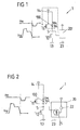
- Figure 1 shows a circuit diagram of a modulated Semiconductor radiation source 100 with a schematic shown discharge pulse control 20 '.
- the circuit shown in FIG. 1 corresponds to the circuit of FIG. 4 except for the discharge pulse control 20 '.
- the transistor 12, which serves as the current source of the circuit is supplied with a voltage signal U 12 at its gate connection. This is modulated in accordance with the data to be transmitted and, moreover, has a peaking signal on the respective rising edge of a voltage pulse.
- the current flowing through the semiconductor radiation source is modulated accordingly, cf. Figure 3.
- Negative peaking pulses U 11 for the falling edge of the current signal are provided on the further transistor 11.
- the transistor 11 is part of a circuit known per se for generating peaking pulses, so that this circuit will not be discussed further.
- the discharge pulse control 20 ′ is via a contact point 5 connected to the cathode of the semiconductor radiation source 100 and also has an electrical connection to one constant potential point 23, here the electrical Dimensions.
- the discharge pulse controller 20 prevents excessive peaking of the falling signal edge of a current pulse by the semiconductor radiation source.
- the discharge pulse control 20 ′ measures the voltage at the semiconductor radiation source 100. When a certain value is reached, the peaking circuit for the falling edge under consideration is deactivated. This prevents further discharge of the semiconductor radiation source from a certain point. This statement corresponds to the fact that the forward voltage U HL of the semiconductor radiation source 100 does not drop too much, in particular does not fall below the range of the linear rise in the current-voltage characteristic curve in FIG. 3.
- the discharge pulse control of FIG. 1 and the voltages that occur are shown in more detail in FIG. 6 in one exemplary embodiment.
- the discharge pulse control has a comparator 20 ′′, which compares the voltage at node 5 with a predetermined voltage value.
- the comparator 20 ′′ has two inputs which are connected to two comparison voltages.
- the voltage U HL of the semiconductor radiation source 100 is present at the first input via the contact point 5. This is compared with a predetermined threshold value.
- the threshold value is set by a DC voltage source DC, which is connected to the second input of the comparator 20 ".
- a control signal is generated which is fed via a connection 15 to a first input of a logic OR element 17 which is connected upstream of the transistor 11 of the peaking circuit.
- the voltage variation U 15 specifies the form of this signal.
- a voltage U 11 ' is present at a second input of the OR element 17 and provides the peaking signal of the switch-off process.
- the two signal voltages U 11 'and U 15 determine the output voltage U 11 , which is present at the transistor 11 via the output of the OR element.
- the mode of operation is explained using the voltages U 12 , U 11 ', U 11 , U 15 and -U HL .
- the voltage U 11 ' is at logic ONE, the voltage U 15 at logic ZERO.
- the voltage U 11 is therefore logically ONE at the output of the OR element 17 and at the transistor 11.
- the transistor 11 blocks in this case.
- the signal U 11 ' is now set to logic ZERO by the peaking circuit after the end of the signal U 12 .
- the logic ZERO signal is thus present at both inputs of the OR element 17.
- the transistor 11 is then conductive.
- the voltage at the semiconductor radiation source 100 can be reduced via the transistor 11.
- the signal U 15 is set to logic ONE by the comparator output. This has the effect that the output of the OR element 17 is also set to logic ONE: the transistor 11 now blocks and further discharge of the semiconductor radiation source 100 is prevented.
- the comparator 20 "thus causes the negative pulse U 11 'to end prematurely.
- the comparator 20 "preferably has a hysteresis which prevents the system from oscillating in the low level while the voltage U HL is close to the predetermined threshold value. Furthermore, the comparator is controlled in such a way that it can only be activated on the switch-off edge of the signal.
- FIG. 2 is a circuit diagram of an alternative modulated semiconductor radiation source 100 with a Clamp circuit 20 can be seen that the discharge pulse control 20 ' of Figure 1 replaced. Otherwise the circuit corresponds to Figure 2 shows the circuit of Figure 1.
- the clamping circuit 20 monitors the forward voltage through the semiconductor radiation source 100. If the voltage falls below a certain forward voltage, ie from a certain value of the forward voltage on the falling edge, the negative current signal pulse I HL (see FIG. 3) no longer flows through the semiconductor radiation source 100, but through the Clamping circuit 20 from. The fact that this negative current pulse does not flow through the semiconductor radiation source 100 prevents the forward voltage at the semiconductor radiation source from being lowered too much or discharging it too much, which would delay a subsequent signal pulse.
- the via the contact point 5 with the cathode Semiconductor radiation source 100 connected clamping circuit 20 has a PNP transistor 21, the emitter of which Contact point 5 with the cathode of the semiconductor radiation source 100 is connected.
- the base of transistor 21 is connected to the negative pole of a DC voltage source 22 connected.
- the positive pole of the DC voltage source 22 is via a Contact point 24 connected to a supply voltage.
- the Collector connection of transistor 21 is on the constant potential point 23.
- the transistor 21 If the voltage U HL at the semiconductor radiation source 100 is now above a certain limit value, which can be set by the strength of the DC voltage source 22, the transistor 21 is blocked. Then no current flows through the transistor 21. However, if the voltage U HL at the semiconductor radiation source 100 falls below this set limit value, the transistor 21 automatically becomes conductive and the current I HL at the semiconductor source 100 flows through the p-channel of the transistor 21 to a constant value Potential point 23 from. This prevents the forward voltage U HL at the semiconductor radiation source 100 from being lowered too far, which would delay the semiconductor radiation source 100 from being switched on again.
- a certain limit value which can be set by the strength of the DC voltage source 22
- the invention is not limited in its implementation the illustrated embodiments.
- the Realization of the clamping circuit according to Figure 2 only exemplary to understand.
Landscapes
- Physics & Mathematics (AREA)
- Optics & Photonics (AREA)
- Electromagnetism (AREA)
- Engineering & Computer Science (AREA)
- Computer Networks & Wireless Communication (AREA)
- Signal Processing (AREA)
- Condensed Matter Physics & Semiconductors (AREA)
- General Physics & Mathematics (AREA)
- Semiconductor Lasers (AREA)
- Digital Transmission Methods That Use Modulated Carrier Waves (AREA)
Abstract
Description
- Figur 1
- ein Schaltbild einer modulierten Halbleiterstrahlungsquelle mit einer schematisch dargestellten Entladepulssteuerung;
- Figur 2
- ein Schaltbild einer modulierten Halbleiterstrahlungsquelle mit einem Ausführungsbeispiel einer Klemmschaltung;
- Figur 3
- eine Strom-Spannungs-Kennlinie einer Halbleiterstrahlungsquelle zusammen mit den zugehörigen Signalpulsformen für Strom, Spannung und Licht;
- Figur 4
- ein Schaltbild einer modulierten Halbleiterstrahlungsquelle gemäß dem Stand der Technik;
- Figur 5
- die zeitliche Abfolge von gepeakten Pulsen in einer Treiberschaltung für eine Halbleiterstrahlungsquelle gemäß dem Stand der Technik; und
- Figur 6
- ein Ausführungsbeispiel einer modulierten Halbleiterstrahlungsquelle mit einer Entladepulssteuerung.
- 1
- Elektrische Schaltung
- 5
- elektrischer Kontaktpunkt
- 11
- Transistor der Peaking-Schaltung
- 12
- Transistor
- 13
- Masse
- 14
- Kontaktpunkt mit Versorgungsspannung
- 15
- Verbindung
- 17
- ODER-Element
- 20
- Klemmschaltung
- 20'
- Entladepulssteuerung
- 20''
- Komparator
- 21
- Transistor
- 22
- Gleichspannungsquelle
- 23
- Masse
- 100
- Halbleiterstrahlungsquelle
- IHL
- Strom durch die Halbleiterstrahlungsquelle 100
- IHL,1
- erste Strompulsform
- IHL,2
- zweite Strompulsform
- UHL
- Spannung an der Halbleiterstrahlungsquelle 100
- UHL,1
- erste Spannungspulsform
- UHL,2
- zweite Spannungspulsform
- LICHTHL
- Lichtstrahlung der Halbleiterstrahlungsquelle 100
- LICHTHL,1
- erste Lichtpulsform
- LICHTHL,2
- zweite Lichtpulsform
- U11
- Spannung an Transistor 11
- U12
- Spannung an Transistor 12
- U11'
- Spannung von Peaking-Schaltung an ODER-Element 17
- U15
- Spannung von Komparator 20'' an ODER-Element 17
- DC
- Gleichspannungsquelle
Claims (12)
- Elektrische Schaltung (1) für eine direkt modulierte Halbleiterstrahlungsquelle mit einer Halbleiterstrahlungsquelle (100), der in Abhängigkeit von einem digitalen Datensignal ein modulierter Strom (IHL) zugeführt wird, dessen abfallende Signalflanke ein Peaking aufweist,
gekennzeichnet durch
Schaltungsmittel (20'; 20), die mit einem elektrischen Kontaktpunkt (5) der Schaltung (1) verbunden sind und bei Unterschreiten eines vorgegebenen Werts der Flussspannung (UHL) an der Halbleiterstrahlungsquelle (100) ein Peaking der abfallenden Signalflanke reduzieren bzw. verhindern. - Schaltung nach Anspruch 1, dadurch gekennzeichnet, dass die Schaltungsmittel (20'; 20) den Strom (IHL) durch die Halbleiterstrahlungsquelle (100) bei Unterschreiten des vorgegebenen Werts der Flussspannung mindestens teilweise umlenken oder abschalten.
- Schaltung nach Anspruch 1 oder 2, dadurch gekennzeichnet, dass der für die Halbleiterstrahlungsquelle (100) bestimmte Strom (IHL) durch die Schaltungsmittel (20) abfließt, wenn die Spannung (UHL) an der Halbleiterstrahlungsquelle (100) den vorgegebenen Wert der Flussspannung unterschreitet.
- Schaltung nach einem der vorangegangenen Ansprüche, dadurch gekennzeichnet, dass die Schaltungsmittel (20) mindestens einen Transistor (21) aufweisen, dessen Basis an einer Gleichspannungsquelle (22) liegt, die den vorgegebenen Wert der Flussspannung festlegt, und dessen Kollektor oder Emitter mit dem elektrischen Kontaktpunkt (5) verbunden ist.
- Schaltung nach Anspruch 4, dadurch gekennzeichnet, dass der Strom durch die Halbleiterstrahlungsquelle bei Unterschreiten des vorgegebenen Werts der Flussspannung durch den Transistor (21) abgeleitet wird.
- Schaltung nach einem der Ansprüche 3 bis 5, dadurch gekennzeichnet, dass die Schaltungsmittel (20) einen PNP-Transistor (21) aufweisen und die Halbleiterstrahlungsquelle (100) eine mit einem festen elektrischen Potential (13) verbundene Kathode aufweist, die mit dem Emitteranschluss des PNP-Transistors (21) verbunden ist.
- Schaltung nach einem der Ansprüche 3 bis 5, dadurch gekennzeichnet, dass die Schaltungsmittel (20) einen NPN-Transistor aufweisen und die Halbleiterstrahlungsquelle (100) eine mit einem festen elektrischen Potential verbundene Anode aufweist, die mit dem Emitteranschluss des NPN-Transistors verbunden ist.
- Schaltung nach einem der vorangegangenen Ansprüche, dadurch gekennzeichnet, dass die Schaltungsmittel eine Entladepulssteuerung (20') aufweisen, die das Peaking der abfallenden Signalflanke mittels einer entsprechenden Steuerung der Peaking-Pulse reduziert.
- Schaltung nach Anspruch 8, dadurch gekennzeichnet, dass die Entladepulssteuerung (20') bei Unterschreiten eines vorgegebenen Werts der Flussspannung einer ein Peaking bereitstellenden Schaltung (11) ein Spannungs- oder Stromsignal zuführen, das ein Abschalten des Peakings der betrachteten Flanke bewirkt.
- Schaltung nach Anspruch 9, dadurch gekennzeichnet, dass die Entladepulssteuerung (20') einen Komparator (20") aufweist, der die Spannung am elektrischen Kontaktpunkt (5) mit einem vorgegebenen Spannungswert vergleicht und bei Unterschreiten des vorgegebenen Werts ein Spannungs- oder Stromsignal erzeugt, das der ein Peaking bereitstellenden Schaltung (11) zugeführt wird.
- Schaltung nach Anspruch 9 oder 10, dadurch gekennzeichnet, dass die ein Peaking bereitstellende Schaltung einen Transistor (11) aufweist und das Spannungsoder Stromsignal einer der Basis des Transistors (11) vorgeschalteten ODER-Schaltung zugeführt wird.
- Schaltung nach einem der vorangegangenen Ansprüche, dadurch gekennzeichnet, dass die Schaltungsmittel (20; 20') eine elektrische Verbindung zu einem konstanten Potentialpunkt (23) aufweisen, insbesondere zu einer elektrischen Masse.
Applications Claiming Priority (2)
| Application Number | Priority Date | Filing Date | Title |
|---|---|---|---|
| DE10320333 | 2003-05-06 | ||
| DE10320333A DE10320333B4 (de) | 2003-05-06 | 2003-05-06 | Elektrische Schaltungen für eine direkt modulierte Halbleiterstrahlungsquelle |
Publications (2)
| Publication Number | Publication Date |
|---|---|
| EP1487242A2 true EP1487242A2 (de) | 2004-12-15 |
| EP1487242A3 EP1487242A3 (de) | 2006-06-14 |
Family
ID=33185718
Family Applications (1)
| Application Number | Title | Priority Date | Filing Date |
|---|---|---|---|
| EP04090160A Withdrawn EP1487242A3 (de) | 2003-05-06 | 2004-04-22 | Elektrische Schaltung für eine direkt modulierte Halbleiterstrahlungsquelle |
Country Status (3)
| Country | Link |
|---|---|
| US (1) | US7224709B2 (de) |
| EP (1) | EP1487242A3 (de) |
| DE (1) | DE10320333B4 (de) |
Families Citing this family (3)
| Publication number | Priority date | Publication date | Assignee | Title |
|---|---|---|---|---|
| US7668464B2 (en) * | 2002-11-06 | 2010-02-23 | Finisar Corporation | Control of peaking of laser driver current to improve eye quality |
| TW567054B (en) * | 2002-11-28 | 2003-12-21 | Actherm Inc | Method for assembling electric clinical thermometer and structure thereof |
| US7170335B2 (en) * | 2004-03-08 | 2007-01-30 | Avago Technologies Ecbu Ip (Singapore) Pte. Ltd. | Driver circuit for driving a light source of an optical pointing device |
Family Cites Families (8)
| Publication number | Priority date | Publication date | Assignee | Title |
|---|---|---|---|---|
| US6018538A (en) * | 1997-06-18 | 2000-01-25 | Lucent Technologies Inc. | High speed non-biased semiconductor laser dione driver for high speed digital communication |
| US6272160B1 (en) * | 1998-02-03 | 2001-08-07 | Applied Micro Circuits Corporation | High-speed CMOS driver for vertical-cavity surface-emitting lasers |
| US6285692B1 (en) * | 1998-08-05 | 2001-09-04 | Advantest Corporation | Method and apparatus for driving laser diode |
| JP2000138415A (ja) * | 1998-11-02 | 2000-05-16 | Fujikura Ltd | 半導体レーザ駆動回路 |
| JP3438779B2 (ja) * | 2000-05-09 | 2003-08-18 | 住友電気工業株式会社 | 駆動回路および半導体レーザ駆動装置 |
| US6947456B2 (en) * | 2000-12-12 | 2005-09-20 | Agilent Technologies, Inc. | Open-loop laser driver having an integrated digital controller |
| DE10065838C2 (de) * | 2000-12-29 | 2003-06-26 | Infineon Technologies Ag | Elektronische Treiberschaltung für einen direkt modulierten Halbleiterlaser |
| DE10218939B4 (de) * | 2002-04-19 | 2005-08-25 | Infineon Technologies Ag | Lasertreiber und Verfahren zur Steuerung der Modulation einer Laserdiode |
-
2003
- 2003-05-06 DE DE10320333A patent/DE10320333B4/de not_active Expired - Fee Related
-
2004
- 2004-04-22 EP EP04090160A patent/EP1487242A3/de not_active Withdrawn
- 2004-05-04 US US10/838,821 patent/US7224709B2/en not_active Expired - Fee Related
Also Published As
| Publication number | Publication date |
|---|---|
| US20040264526A1 (en) | 2004-12-30 |
| DE10320333B4 (de) | 2009-06-18 |
| US7224709B2 (en) | 2007-05-29 |
| DE10320333A1 (de) | 2004-12-09 |
| EP1487242A3 (de) | 2006-06-14 |
Similar Documents
| Publication | Publication Date | Title |
|---|---|---|
| DE112007000857B4 (de) | Drei Treiberschaltungen für Halbleiterelemente mit Kurzschlusserfassung | |
| DE69311755T2 (de) | Steuerschaltung für lichtemittierende Vorrichtung | |
| DE69529494T2 (de) | Steuerschaltung für Halbleitervorrichtung | |
| DE4008376C2 (de) | ||
| DE10048433B4 (de) | Lastbetätigungsschaltkreis | |
| DE19533116A1 (de) | Treiberschaltung für eine Leuchtdiode | |
| DE2514462C3 (de) | Schaltungsanordnung zur Umwandlung eines Spannungspegels | |
| DE2900539C3 (de) | Logische Schaltung | |
| DE1248104B (de) | Elektro-optische Kippschaltung | |
| EP0137055B1 (de) | Schaltnetzteil mit Überstromschutz | |
| DE3587924T2 (de) | Schaltung zur Beschleunigung des Hoch-Tief-Überganges für TTL-Gatter. | |
| DE102005003643B4 (de) | Schaltungsvorrichtung mit einem Strombegrenzer eines Ausgangstransistors | |
| EP0013710B1 (de) | Gegentakt-Treiberschaltung, deren Ausgang direkt mit den Ausgängen weiterer Treiberschaltungen verknüpfbar ist | |
| EP0314013B1 (de) | Verfahren zur Basisstromregelung eines Schalttransistors und Schaltungsanordnung zur Durchführung des Verfahrens | |
| DE2030135C3 (de) | Verknüpfungsschaltung | |
| EP0698794A1 (de) | Schaltungsanordnung zur Unterspannungs-Erkennung | |
| DE1186502B (de) | Schaltung zur Sperrung von Eingangsimpulsen, die eine kuerzere Zeitdauer als eine vorherbestimmte minimale Zeitdauer aufweisen | |
| DE10320333B4 (de) | Elektrische Schaltungen für eine direkt modulierte Halbleiterstrahlungsquelle | |
| DE10215363A1 (de) | Schaltungsanordnung zum Ansteuern eines Halbleiterschalters | |
| DE102020131358A1 (de) | Halbleitervorrichtung | |
| DE10143432C1 (de) | Treiberschaltung und Ansteuerverfahren für einen feldgesteuerten Leistungsschalter | |
| DE102009045220A1 (de) | System und Verfahren zum Begrenzen von Stromoszillationen | |
| DE102023108243A1 (de) | Laserdiodentreiber und verfahren zum betreiben eines optoelektronischen baueelements | |
| DE102014010202B3 (de) | EMV gerechte Flanken-Regelung für Transceiver eines Eindrahtbussystems, insbesondere für einen LINBUS-Transceiver | |
| DE3536447C2 (de) | Kurzschluß- und überlastfeste Transistorausgangsstufe |
Legal Events
| Date | Code | Title | Description |
|---|---|---|---|
| PUAI | Public reference made under article 153(3) epc to a published international application that has entered the european phase |
Free format text: ORIGINAL CODE: 0009012 |
|
| AK | Designated contracting states |
Kind code of ref document: A2 Designated state(s): AT BE BG CH CY CZ DE DK EE ES FI FR GB GR HU IE IT LI LU MC NL PL PT RO SE SI SK TR |
|
| AX | Request for extension of the european patent |
Extension state: AL HR LT LV MK |
|
| PUAL | Search report despatched |
Free format text: ORIGINAL CODE: 0009013 |
|
| AK | Designated contracting states |
Kind code of ref document: A3 Designated state(s): AT BE BG CH CY CZ DE DK EE ES FI FR GB GR HU IE IT LI LU MC NL PL PT RO SE SI SK TR |
|
| AX | Request for extension of the european patent |
Extension state: AL HR LT LV MK |
|
| RIC1 | Information provided on ipc code assigned before grant |
Ipc: H05B 33/08 20060101ALN20060509BHEP Ipc: H01S 5/042 20060101AFI20060509BHEP |
|
| AKX | Designation fees paid | ||
| STAA | Information on the status of an ep patent application or granted ep patent |
Free format text: STATUS: THE APPLICATION IS DEEMED TO BE WITHDRAWN |
|
| 18D | Application deemed to be withdrawn |
Effective date: 20061215 |
|
| REG | Reference to a national code |
Ref country code: DE Ref legal event code: 8566 |