EP1489667A2 - Procedé de passivation de la surface arrière de cellules solaires et cellules solairer avec une telle passivation - Google Patents
Procedé de passivation de la surface arrière de cellules solaires et cellules solairer avec une telle passivation Download PDFInfo
- Publication number
- EP1489667A2 EP1489667A2 EP04447148A EP04447148A EP1489667A2 EP 1489667 A2 EP1489667 A2 EP 1489667A2 EP 04447148 A EP04447148 A EP 04447148A EP 04447148 A EP04447148 A EP 04447148A EP 1489667 A2 EP1489667 A2 EP 1489667A2
- Authority
- EP
- European Patent Office
- Prior art keywords
- oxide
- solar cell
- tio
- metal
- metalloid
- Prior art date
- Legal status (The legal status is an assumption and is not a legal conclusion. Google has not performed a legal analysis and makes no representation as to the accuracy of the status listed.)
- Withdrawn
Links
Images

Classifications
-
- H—ELECTRICITY
- H10—SEMICONDUCTOR DEVICES; ELECTRIC SOLID-STATE DEVICES NOT OTHERWISE PROVIDED FOR
- H10F—INORGANIC SEMICONDUCTOR DEVICES SENSITIVE TO INFRARED RADIATION, LIGHT, ELECTROMAGNETIC RADIATION OF SHORTER WAVELENGTH OR CORPUSCULAR RADIATION
- H10F71/00—Manufacture or treatment of devices covered by this subclass
- H10F71/129—Passivating
-
- H—ELECTRICITY
- H10—SEMICONDUCTOR DEVICES; ELECTRIC SOLID-STATE DEVICES NOT OTHERWISE PROVIDED FOR
- H10F—INORGANIC SEMICONDUCTOR DEVICES SENSITIVE TO INFRARED RADIATION, LIGHT, ELECTROMAGNETIC RADIATION OF SHORTER WAVELENGTH OR CORPUSCULAR RADIATION
- H10F77/00—Constructional details of devices covered by this subclass
- H10F77/30—Coatings
- H10F77/306—Coatings for devices having potential barriers
- H10F77/311—Coatings for devices having potential barriers for photovoltaic cells
-
- Y—GENERAL TAGGING OF NEW TECHNOLOGICAL DEVELOPMENTS; GENERAL TAGGING OF CROSS-SECTIONAL TECHNOLOGIES SPANNING OVER SEVERAL SECTIONS OF THE IPC; TECHNICAL SUBJECTS COVERED BY FORMER USPC CROSS-REFERENCE ART COLLECTIONS [XRACs] AND DIGESTS
- Y02—TECHNOLOGIES OR APPLICATIONS FOR MITIGATION OR ADAPTATION AGAINST CLIMATE CHANGE
- Y02E—REDUCTION OF GREENHOUSE GAS [GHG] EMISSIONS, RELATED TO ENERGY GENERATION, TRANSMISSION OR DISTRIBUTION
- Y02E10/00—Energy generation through renewable energy sources
- Y02E10/50—Photovoltaic [PV] energy
-
- Y—GENERAL TAGGING OF NEW TECHNOLOGICAL DEVELOPMENTS; GENERAL TAGGING OF CROSS-SECTIONAL TECHNOLOGIES SPANNING OVER SEVERAL SECTIONS OF THE IPC; TECHNICAL SUBJECTS COVERED BY FORMER USPC CROSS-REFERENCE ART COLLECTIONS [XRACs] AND DIGESTS
- Y02—TECHNOLOGIES OR APPLICATIONS FOR MITIGATION OR ADAPTATION AGAINST CLIMATE CHANGE
- Y02P—CLIMATE CHANGE MITIGATION TECHNOLOGIES IN THE PRODUCTION OR PROCESSING OF GOODS
- Y02P70/00—Climate change mitigation technologies in the production process for final industrial or consumer products
- Y02P70/50—Manufacturing or production processes characterised by the final manufactured product
-
- Y—GENERAL TAGGING OF NEW TECHNOLOGICAL DEVELOPMENTS; GENERAL TAGGING OF CROSS-SECTIONAL TECHNOLOGIES SPANNING OVER SEVERAL SECTIONS OF THE IPC; TECHNICAL SUBJECTS COVERED BY FORMER USPC CROSS-REFERENCE ART COLLECTIONS [XRACs] AND DIGESTS
- Y10—TECHNICAL SUBJECTS COVERED BY FORMER USPC
- Y10T—TECHNICAL SUBJECTS COVERED BY FORMER US CLASSIFICATION
- Y10T428/00—Stock material or miscellaneous articles
- Y10T428/31504—Composite [nonstructural laminate]
- Y10T428/31678—Of metal
Definitions
- the present invention relates to semiconductor devices such as solar cells, e.g. silicon solar cells, and more particularly to a method for passivation of a semiconductor substrate surface, e.g. silicon surface of a solar cell by a dielectric with negative fixed charge at the interface between the semiconductor substrate, e.g. silicon, and a passivating dielectric.
- Solar cells convert impinging electromagnetic radiation, e.g. sunlight directly into electrical energy. They are made of semiconducting materials which can be monocrystalline, polycrystalline or amorphous. This process of converting light (photons) to electrical energy (voltage) is called the photovoltaic (PV) effect. The performance of a solar cell is measured in terms of its efficiency at turning light energy into electrical energy.
- the thickness can be so low that minority carriers will easily reach the back surface of the solar cell and will recombine there. Through this, a significant loss of energy occurs and only a small amount of the impinging sunlight is effectively converted into electrical energy.
- An alternative is to increase the thickness of semiconductor material with its cost disadvantages.
- a layer also called a back surface field (BSF) passivation layer, has been created at the back side of the solar cell by diffusion of dopants at the back side, in order to stop recombination and to allow minority carriers to diffuse back to the junction formed by the interface between the semiconductor, e.g. silicon, and the passivating layer, and to subsequently contribute to the cell's current.
- BSF back surface field
- the p + region at the cell back results in injection of holes into the back of p-type silicon, creating a high density of holes at the boundary of the bulk.
- the p + region at the back constitutes a barrier to the movement of electrons to the back contact (Fig.1a), and in this way a reduction in the rear surface recombination velocity is reached.
- This effect is still rather inappropriately referred to as the back surface field (BSF) effect.
- BSF back surface field
- the use of a p + region requires an additional doping with acceptor-type impurities which means more technological steps and costs raising.
- a thin dielectric film which has a big fixed charge of a first type, e.g. a negative charge, at the dielectric/semiconductor interface (Fig. 1b).
- a first type e.g. a negative charge
- a second type opposite to the first type
- MIS metal insulator semiconductor
- FIG. 2a an energy band diagram of such an MIS structure is shown for a p-type semiconductor.
- a MIS structure With an MIS structure equilibrium will be established when the Fermi levels are aligned. Fermi level alignment involves charge movement and since charge cannot move through the dielectric (insulator), an external connection between the semiconductor and the metal is necessary in order to allow equilibrium.
- ⁇ ms ⁇ m -( ⁇ +E g /2+ ⁇ B )
- ⁇ m the metal work function
- ⁇ the semiconductor electron affinity
- E g the band gap
- ⁇ B the bulk potential
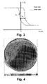
- Fig. 3 the high frequency current-voltage (CV) curves for an ideal and a real MIS structure are shown, by means of a dashed and a full line respectively.
- CV current-voltage
- a first known passivation layer for a silicon semiconductor layer is a SiO 2 layer. It is known that SiO 2 has excellent passivation properties on silicon. This is based on proper surface termination, although it is known that SiO 2 accumulates positive charges at the interface.
- SiN x :H local BSF is used as passivation layer for silicon surfaces.
- This technology is often employed on development solar cells. It relies on field induced passivation, through the accumulation of a high density of positive charges at the interface with silicon. On p-silicon substrates this generates an inversion layer which acts as an induced floating junction, which has not the effect of BSF.
- a disadvantage of this solution is that it is costly and relatively elaborate.
- dielectrics of the above described type When dielectrics of the above described type are deposited on p-type silicon, they induce an accumulation layer and a reduction of the effective surface recombination velocity is anticipated.
- the band bending due to this negative charge provides a very effective field induced surface passivation, on high and, remarkably, on low resistivity wafers too, making it a superior choice with respect to diffused BSF.
- the material quality in the drift field region is preserved, as there is no indiffusion of dopant species or impurities, nor formation of bulk defects typical of highly doped perturbed lattices.
- dielectrics with a high positive charge e.g. standard SiNx:H
- field passivation is due to an inversion layer which needs to be floating and is very sensitive to parasitic shunting, no contact separation is needed.
- the present invention provides a method for surface passivation of a semiconductor device, comprising applying an oxide system at a surface of the semiconductor device.
- the semiconductor device can be a solar cell, e.g. a silicon solar cell.
- the oxide system comprises at least two oxides, i.e. Al 2 O 3 and at least one metal oxide, such as e.g. TiO 2 or ZrO 2 , or metalloid (semi-metal) oxide, such as e.g. SiO 2 .
- the additional oxide preferably enhances the tetrahedral structure of Al 2 O 3 . The effect is to provide a passivation layer with negative fixed charge.
- the oxide system may be a binary oxide system comprising Al 2 O 3 and a metal oxide or metalloid (semi-metal) oxide which enhances the tetrahedral structure of Al 2 O 3 .
- Al 2 O 3 can have two forms, if which the tetrahedral from is less common but it is this form that has the right charge for surface passivation of semiconductor solar cells according to the present invention.
- the method according to the present invention has several advantages over the prior art.
- the deposition process is potentially low-cost and does not require expensive equipment.
- the process is very reproducible, due to the fact that the developed process is not critical to the technological conditions.
- it is not necessary to deposit an intermediate SiO 2 -layer and the use of fluorine can be avoided with all the environmental and processing benefits thereof.
- the oxide system may comprise a mixture of Al 2 O 3 and the at least one metal oxide or metalloid oxide.
- the Al 2 O 3 may be mixed with one or more metal oxides and/or with one or more metalloid oxides.
- the Al 2 O 3 is mixed with just one metal oxide or metalloid oxide.
- Compound systems or mixtures used in a method according to the present invention are combinations of two or more oxides. These alloy systems are predominantly non-stoichiometric mixtures and are therefore, in the case of a mixture of two materials, termed pseudobinary alloys (see paper of G. Wilk et al J. Appl. Physics v.89, 10, p.3262, 2001). In this way, it is possible to vary the ratio of the plurality of oxides and to obtain thin films with certain pre-set characteristics, such as refractive index, extinction coefficient, energy band gap, dielectric constants, etc.
- non-stoichiometric mixtures of Al 2 O 3 and the at least one metal oxide and/or metalloid oxide may be used as a passivating layer for surface passivation of a semiconductor device such as a solar cell, e.g. pseudobinary alloys (also called pseudobinaries), comprising an Al 2 O 3 component and a metal oxide or metalloid oxide which enhances the tetrahedral structure of Al 2 O 3 .
- pseudobinary alloys also called pseudobinaries
- the passivating layer may consist of a pseudobinary (Al 2 O 3 ) x (TiO 2 ) 1-x alloy, comprising a mixture of Al 2 O 3 and TiO 2 .
- the mixture may have a fixed ratio of Al 2 O 3 to the metal oxide or metalloid oxide, e.g. a fixed ratio of Al 2 O 3 : TiO 2 .
- the mixture of two or more oxides either a stoichiometric or a non-stoichiometric mixture, may be prepared by a sol-gel method.
- applying the oxide system may comprise spin-coating on the oxide system.
- the present invention furthermore provides a semiconductor device such as a solar cell having backside surface passivation.
- the semiconductor device such as a solar cell comprises a semiconductor substrate having a major surface and an oxide system on the major surface, the oxide system comprising Al 2 O 3 and at least one metal oxide and/or metalloid oxide which enhances the tetrahedral structure of Al 2 O 3 .
- the oxide system may be a binary oxide system comprising Al 2 O 3 and a metal oxide or metalloid (semi-metal) oxide which enhances the tetrahedral structure of Al 2 O 3 .
- the oxide system may comprise more than two oxides, for example, in the case of three oxides, Al 2 O 3 and two metal oxides, or Al 2 O 3 and two metalloid oxides, or Al 2 O 3 , one metal oxide and one metalloid oxide.
- the oxide system may comprise a mixture of Al 2 O 3 and the at least one metal oxide, e.g. TiO 2 or ZrO 2 , and/or metalloid oxide, e.g. SiO 2 .
- the mixture may be a stoichiometric mixture.
- the mixture may be a non-stoichiometric mixture, which in case of a mixture of two oxides is called a pseudobinary alloy (also called a pseudobinary), which comprises an Al 2 O 3 component and at least one metal oxide and/or metalloid oxide. In this way it is possible to combine the desirable properties from the different oxides, while eliminating the undesirable properties of each individual material.
- a pseudobinary alloy also called a pseudobinary
- the mixture may be a pseudobinary alloy at a fixed ratio of Al 2 O 3 to the metal oxide or metalloid oxide, e.g. a fixed ratio of Al 2 O 3 :TiO 2 .
- the solar cell may further comprise a backside metal contact.
- This backside metal contact may be a metal grid direct on the semiconductor, e.g. p-type silicon, substrate or a metal reflector.
- the present invention will be described with reference to solar cells but the present invention is not limited thereto.
- the invention may be applied to any form of semiconductor product.
- solar cells and a method for passivating a surface of a semiconductor solar cell are provided by using dielectrics which accumulate charge of a first type, e.g. negative charge, at the dielectric/semiconductor interface.
- This passivating method may be applied to any semiconductor device.
- Al 2 O 3 layers were used as a passivating layer.
- Al 2 O 3 layers were deposited by atomic layer deposition (ALD) on both sides of 2 Ohm.cm, 8" CZ-Si wafers.
- ALD atomic layer deposition
- This growth technique may provide atomic layer control and allows conformal films to be deposited on very high aspect ratio structures.
- ALD is based on sequential, self-limiting surface chemical reactions.
- the binary reaction 2Al(CH 3 ) 3 + 3H 2 O ⁇ Al 2 O 3 + 6CH 4 can be split in the following two surface half reactions: AlOH* + Al(CH 3 ) 3 ⁇ AlOAl(CH 3 ) 2 * + CH 4 and AlCH 3 * + H 2 O ⁇ AlOH* + CH 4 where the asterisks denote the surface species.
- Al(CH 3 ) 3 reacts with the hydroxyl species (OH*) and produces a dimethylaluminum covered surface.
- H 2 O reacts with the AlCH3* species and rehydroxilates the surface. An excess of precursors is applied during each half reaction, so they proceed until all sterically available surface species have reacted.
- each reaction is self-limiting, and Al 2 O 3 deposition occurs with atomic layer control.
- Half-reactions (2) and (3) are repeated until an Al 2 O 3 layer of the desired thickness is achieved.
- the full process never reaches temperatures above 300°C, making it de facto a low-temperature process, harmless to the substrates and with a low thermal budget.
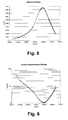
- Fig. 5 and 6 respectively represent the injection dependent lifetime measured with QSSPC and the (conservative value for) surface recombination velocity calculated assuming a bulk lifetime of 2 ms. Throughout the whole range of operation of a solar cell, the surface recombination velocity is in the order of 100 cm/s, reaching a minimum of 10 cm/s at an injection level of 10 15 cm -3 . No degradation of the surface passivation properties has been observed after prolonged high temperature treatments (up to 820°C for 60 minutes).
- a high density of charge resulted to be crucial for proper surface passivation. Measurements carried out on samples with a density of charge less than 10 11 cm -2 resulted in a more modest performance.
- the fixed negative charge at the interface for the considered sample, as calculated from C-V measurements, is about -1.3 x 10 12 cm -2 . Values as high as -1 x 10 13 cm -2 can be obtained.
- This net negative charge is consistent with a model for the local atomic bonding of non-crystalline Al 2 O 3 that has two different bonding environments for the Al atoms, as described by G. Lukovsky et al in Proc. of the Characterisation and Metrology for ULSI Technology, 154-158 (2000).
- the dielectric can be described as a modified continuous random network including a charged network and discrete ions.
- the Al 3+ ions occupy octahedral interstitial sites of the network, and form three resonating, partially covalent donor-acceptor pair bonds with bridging oxygen atoms of that network.
- the reason for the negative charge at the Al 2 O 3 /Si interface is that the Al ions rearrange in tetrahedrally co-ordinated Al sites with a net negative charge bonded directly to the O atoms of the SiO 2 interfacial. Thermal or 'firing' conditions typical for solar cell processing do not affect the passivation properties of optimised layers.
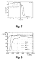
- the net amount of fixed negative charge remains substantially stable, if it is not even increased (see Fig. 7).
- the surface recombination velocity remains in the same order of magnitude. No significant degradation of the layers has been shown over a period of 6 months.
- the increase of the flat-band shift in the annealed sample, as illustrated in Fig. 7, indicates an increased negative interface charge density.
- Al 2 O 3 layers formed as described above, thus seem to be suitable for surface passivation of the base of crystalline silicon solar cells.
- Atomic Layer Deposition is less preferable for industrial, large scale production. The layers are rather difficult to structure and the throughput of the system is very low.
- the present invention provides the use of a combination or mixture of two or more oxides for use as a passivation layer, one of the oxides being Al 2 O 3 and the other at least one oxide being a metal oxide or metalloid oxide which enhances the tetrahedral structure of Al 2 O 3 .
- These mixtures or alloy systems may be predominantly non-stoichiometric mixtures and are called, in the case of a mixture of two materials, pseudobinary alloys (PBAs). They allow combining the desirable properties of the different oxides in order to obtain a dielectric system consisting of a thin film with certain pre-set values - refractive index, extinction coefficient, energy band gap, dielectric constants, ... and negative or positive trapped charges.
- PBAs pseudobinary alloys
- a binary oxide system such as e.g. a pseudobinary alloy of the type (Al 2 O 3 ) x (TiO 2 ) 1-y , is used as a passivating layer.
- formation of the pseudobinary alloy may be carried out by a sol-gel method.
- Liquid phase deposition of thin dielectric films obtained by the sol-gel method has been actively used for several years in research laboratories for fabrication of optical devices and components.
- Recently, the technique has also demonstrated its potential for commercial manufacturing in various fields of application in semiconductor industry. Particular advantages are achieved with alloys of two metal oxides, i.e. with pseudobinary alloys.
- the first step in the preparation of a (Al 2 O 3 ) x (TiO 2 ) 1-x alloy is the formation of a titanium dioxide sol.
- a titanium ethoxide may for example be used as a titanium precursor to form the TiO 2 films.
- other suitable precursors can be used here.
- acetic acid C 2 H 5 OH preferably having a purity of at least 96 %, to the titanium precursor an exothermic reaction is caused.
- Acetate modification was performed in-situ by introducing of for example 1.5 mg, or any suitable amount, of glacial acetic acid.
- the process is exothermal and, keeping in mind the great difference in the stability constants of the two complexes, it leads to full substitution of alcoxic groups by the more stable acetic groups.
- Subsequent addition of a small amount of water, such as for example 60 mol, or any suitable amount, of water causes hydrolysis and a condensation reaction and results in gelation of the solution and the formation of a transparent gel.
- the addition of for example 1 mol, or any suitable amount, of acetylaceton leads to peptisation of the gel.
- a stirring at low revolutions (100-150 rpm) follows.
- a next step is the preparation of the aluminum sol.
- an organic aluminium source such as Aluminum chloride anhydrous Al[OCH(CH) 3 ) 2 ] 3 . This is preferably dissolved in a suitable solvent such as for example absolute ethanol.
- a suitable solvent such as for example absolute ethanol.
- the reaction is exothermal and could be explained as follows: AlCl 3 + 3C 2 H 3 OH ⁇ Al(C 2 H 5 O) 3 + 3 HCl
- the obtained solution preferably has a pH in the range of 1 - 1.2.
- the presence of HCl is appropriate for this invention because the gettering effect of chlorine for undesirable metal impurities is well known. The latter are the main reason for decreasing the lifetime of minority carriers on Si surface.
- chlorine decreases the surface states density when thermal SiO x is grown on the Si surface.
- both sols are mixed in suitable ratios and solutions with different aluminum contents may be produced.
- the ratios of the two oxide components can be altered by varying the quantity of the two precursors in the sol solutions.
- the Ti sol and Al solutions are carefully mixed together under mechanical agitation. Examples of mechanical agitation are stirring and ultrasonic treatment.
- the temperature is preferably maintained at 40°C.
- By increasing the content of Al in the solution thus by increasing the concentration of the Al[OCH(CH) 3 ) 2 ] 3 compound, higher Al/Ti rations can be obtained in the (Al 2 O 3 ) x (TiO 2 ) 1-x alloy, which has an advantage as explained below.
- the working solution is finally obtained after series of treatments in order to get homogeneous and filtered product, which is suitable for thin film deposition, for example using spin-coating technique.
- the sols prepared according to this embodiment are stable for more than 5 months.
- the precursor used for the aluminium component may be an inorganic one such as e.g. AlCl 3 anhydrous, also dissolved in a solvent, e.g. absolute ethanol.
- a solvent e.g. absolute ethanol.
- the (Al 2 O 3 ) x (TiO 2 ) 1-x alloy can be deposited onto the silicon substrate by any suitable method. Spin coating is a preferred method.
- the (Al 2 O 3 ) x (TiO 2 ) 1-x , alloy is deposited on a polished single crystal p-silicon wafer with orientation ⁇ 100>.
- the layer deposition process may comprise the following steps.
- a first step is a chemical cleaning process for the semiconductor substrate, e.g. silicon substrate. Therefore the substrate may e.g. be dipped in a H 2 SO 4 : H 2 O 2 (1:1 ) solution for 30 min. Because of the oxidising nature of the chemicals, a native oxide layer is formed. Therefore, the next step in the cleaning process may be an oxide etching in HF 1:10 and subsequently rinsing in deionised water. As for this step fluorine is used in diluted quantities and because it is followed by a rinse step, no environmental pollution will occur. Finally the substrate is treated again in H 2 SO 4 : H 2 O 2 (1:1) solution in order to form a very thin SiO 2 film with 1 nm thickness. The oxide film formed during this treatment is the result of a chemical cleaning which leaves a monolayer (or few monolayers) of oxide on the surface. This is called a native oxide and is useful for the growth/deposition of the pseudobinary alloy.
- the thin (Al 2 O 3 ) x (TiO 2 ) 1-x ), film is deposited onto the silicon substrate e.g. by spin coating with preferably 6000 to 8000 rpm for 30 sec.
- the layer's thickness depends on the ratio Al: Ti in the sol solution and is in the range of 40 - 70 nm.
- the samples are then dried, e.g. at 80 ⁇ 5°C for 30 min, in order to obtain a xerogel film and to remove residual solvents.
- Organic components are then pyrolised, e.g. by firing at 350 ⁇ 10°C in O 2 for 1 hour.
- a last step in the layer deposition process is high temperature annealing, e.g.
- the (Al 2 O 3 ) x (TiO 2 ) 1-x alloy layer deposited according to this embodiment, is dense, homogenous and smooth with good thickness uniformity of ⁇ 1% along the wafer. Preferably no pores, inhomogeneity or pinholes exist in the layer.
- Table 1 shows the results on fixed oxide charge of films deposited from 3 different sol solutions according to the above described embodiment.
- the different solutions contain increasing Al contents as follows:
- the thin films are deposited on p-type Si substrates and 2" sapphire.
- Refractive index, n and thicknesses d of the films were calculated simultaneously by minimization of the objective function F including sum of measured and calculated transmissions: where N is the number of points in the transparent range of each layer over which the summation is performed.
- n 2 1+ E d E 0 E 2 0 - E 2
- E d and E 0 are the dispersion and single-oscillator energies, respectively and E - the photon energy.
- the initial estimates for E d and E 0 taken from the literature as well as the thickness are varied until a good fit between the measured and calculated values of T is found.
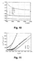
- Fig. 10 presents the spectral dependencies of the refractive indices for some layers.
- n obeys weak dispersion and decreases slowly when ⁇ increases.
- the influence of x is much pronounced: the refractive index grows with the decrease of x.
- the charge of the first type being a negative fixed oxide charge is characteristic for all the annealed films described above. With increasing Al content of the solution the negative charge N f increases. N f [cm -2 ] Sol solution Type Al 1 - 4.9 * 10 11 Sol solution Type Al 1.5 - 5.2 * 10 11 Sol solution Type Al 2 - 6.6 * 10 11
- the (Al 2 O 3 ) x (TiO 2 ) 1-x alloy is deposited onto an unpolished single crystal p-silicon wafer.
- the (Al 2 O 3 ) x (TiO 2 ) 1-x film is uniformly deposited onto the surface and follows the relief of the substrate.
- the films, which were deposited on these unpolished single crystal p-silicon wafers, were with effective thickness two times thinner than on polished Si-substrates.
- the (Al 2 O 3 ) x (TiO 2 ) 1-x alloy is deposited onto a polycrystalline silicon wafer.
- the deposited film represents a uniform coating without inhomogeneities along the depth.
- the (Al 2 O 3 ) x (TiO 2 ) 1-x layer shows no substantial difference in the film thickness, the film coats the substrate uniformly. The thickness of the layer is smaller as compared to that of the polished substrates.
- the used Si substrates were p-type ⁇ 100>, unpolished p-Si and multicrystalline Si.
- Hg probe is used. This case is closer to the situation, when the dielectric layer is utilized for surface passivation.
- the overall dielectric permittivity of the pseudobinary alloy (Al 2 O 3 ) x (TiO 2 ) 1-x is always lower than that of pure TiO 2 but it results from Al 2 O 3 component presence.
- the dielectric constant decreases with the increase of the component with low dielectric constant - aluminum oxide (Table 4). This is another demonstration of the fact that combining different oxides a multicomponent oxide layer with varying physical properties is obtained.
- the refractive indices do not depend on the film thickness and the temperature treatments.
- the films annealed at 750°C possibly become denser and for that reason their thickness is 12% lower than that of the films annealed at 650°C.
- the given values are the average from 5 points measurements.
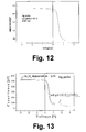
- the silicon substrate is in accumulation (Fig. 12).
- the thickness of CVD Al 2 O 3 film is 10 nm, correspondingly the thickness of pseudobinary alloy is 46 nm.
- the upper electrode is a Hg probe. It is to be noted that no differences in capacitance of accumulation region are observed, although the great difference in thickness. For ALD CVD 10 nm thick film, this effect is connected with the small value of the effective dielectric constant.
- sol solutions are developed which allow to deposit, e.g. by spin-coating, a pseudobinary alloy (ZrO 2 ) x (Al 2 O 3 ) 1-x .
- a pseudobinary alloy ZrO 2 ) x (Al 2 O 3 ) 1-x .
- Such thin film can be obtained on Si wafers with different thicknesses as a result of multiple spin coating procedures. After low temperature (350°C) and high temperature (750°C) annealing, homogeneous thin films are obtained with no visual defects.
- the back side of the wafers is preferably covered with an Al layer to get ohmic contact with the substrate, e.g. Si.
- the capacitance - voltage characteristics of the dielectric/Si structures as mentioned above have been measured by Hg probe with area 4.8x10 -3 cm 2 .
- Table 8 gives the results from the measurements of the fixed oxide charge and the dielectric constant. The highest "negative" charge values are obtained for films, containing Al 2 O 3 .
- the D f value for (ZrO 2 ) x (Al 2 O 3 ) 1-x film is 4.5x10 11 cm -2
- a high dielectric constant ( ⁇ ) is obtained for (ZrO 2 ) x (Al 2 O 3 ) 1-x film, which makes it promising material for high - k dielectric.
- the amorphous films, formed by the method of the present invention show the following properties:
- the method according to the invention shows several advantages with respect to the prior art.
- the deposition process is low-cost, uses an easy technology and does not require expensive equipment. Furthermore, a high reproducibility of the results may be achieved, due to the fact that the developed process is not critical to the technological conditions. Moreover, the process according to the invention does not need gases or hazard chemicals and hence, is respectively safe and ecological.
- an alloy of aluminum oxide with a metal or metalloid oxide is an ideal candidate for high-quality surface passivation of p-type silicon and solar cells application.
- the net negative fixed charge at its interface with silicon induces an accumulation layer which inherently provides a degree of field induced surface passivation.
Landscapes
- Formation Of Insulating Films (AREA)
Priority Applications (1)
| Application Number | Priority Date | Filing Date | Title |
|---|---|---|---|
| EP20040447148 EP1489667A3 (fr) | 2003-06-20 | 2004-06-21 | Procedé de passivation de la surface arrière de cellules solaires et cellules solairer avec une telle passivation |
Applications Claiming Priority (5)
| Application Number | Priority Date | Filing Date | Title |
|---|---|---|---|
| EP03447168 | 2003-06-20 | ||
| EP03447168 | 2003-06-20 | ||
| GB0401703A GB0401703D0 (en) | 2004-01-27 | 2004-01-27 | Method for backside surface passivation of solar cells and solar cells with such passivation |
| GB0401703 | 2004-01-27 | ||
| EP20040447148 EP1489667A3 (fr) | 2003-06-20 | 2004-06-21 | Procedé de passivation de la surface arrière de cellules solaires et cellules solairer avec une telle passivation |
Publications (2)
| Publication Number | Publication Date |
|---|---|
| EP1489667A2 true EP1489667A2 (fr) | 2004-12-22 |
| EP1489667A3 EP1489667A3 (fr) | 2014-12-03 |
Family
ID=34105767
Family Applications (1)
| Application Number | Title | Priority Date | Filing Date |
|---|---|---|---|
| EP20040447148 Withdrawn EP1489667A3 (fr) | 2003-06-20 | 2004-06-21 | Procedé de passivation de la surface arrière de cellules solaires et cellules solairer avec une telle passivation |
Country Status (2)
| Country | Link |
|---|---|
| US (1) | US7659475B2 (fr) |
| EP (1) | EP1489667A3 (fr) |
Cited By (16)
| Publication number | Priority date | Publication date | Assignee | Title |
|---|---|---|---|---|
| US7375378B2 (en) | 2005-05-12 | 2008-05-20 | General Electric Company | Surface passivated photovoltaic devices |
| WO2009062882A3 (fr) * | 2007-11-14 | 2010-07-08 | Institut Für Solarenergieforschung Gmbh | Procédé de fabrication d'une cellule solaire comportant une double couche de diélectrique à passivation de surface, et cellule solaire correspondante |
| WO2012024736A1 (fr) * | 2010-08-25 | 2012-03-01 | The Australian National University | Procédé de fabrication de semi-conducteur et article à semi-conducteur |
| EP2494605A2 (fr) * | 2009-10-27 | 2012-09-05 | Varian Semiconductor Equipment Associates, Inc. | Réduction de la recombinaison superficielle et amélioration de la capture de la lumière dans les cellules solaires |
| WO2011144207A3 (fr) * | 2010-05-18 | 2012-09-13 | Q-Cells Se | Procédé de production d'un dispositif à semi-conducteur |
| DE102012102745A1 (de) | 2011-07-29 | 2013-01-31 | Schott Solar Ag | Verfahren zur Herstellung einer Solarzelle sowie Solarzelle |
| EP2130230A4 (fr) * | 2007-03-23 | 2013-06-19 | Lg Electronics Inc | Cellule solaire comportant une couche réfléchissante arrière composée d'un diélectrique à k élevé |
| EP2448002A3 (fr) * | 2010-10-29 | 2013-10-30 | Industrial Technology Research Institute | Structure de couche de passivation de dispositif semi-conducteur et procédé de formation associé |
| WO2012171682A3 (fr) * | 2011-06-15 | 2013-11-21 | Robert Bosch Gmbh | Procédé de fabrication d'un dispositif à semi-conducteur |
| WO2013180857A1 (fr) * | 2012-05-31 | 2013-12-05 | Dow Corning Corporation | Plaquette de silicium revêtue d'une couche de passivation |
| EP2398044A3 (fr) * | 2010-06-17 | 2014-07-02 | Katholieke Universiteit Leuven, K.U.L. Leuven R&D | Procédé de passivation d'une surface en silicone |
| RU2532137C2 (ru) * | 2009-09-18 | 2014-10-27 | Син-Эцу Кемикал Ко., Лтд. | Солнечный элемент, способ изготовления солнечного элемента и модуль солнечных элементов |
| US9040983B2 (en) | 2010-10-29 | 2015-05-26 | Industrial Technology Research Institute | Passivation layer structure of semiconductor device and method for forming the same |
| WO2016022026A1 (fr) * | 2014-08-04 | 2016-02-11 | Asm International N.V. | Cellule photovoltaïque à couche de passivation ainsi que procédé de fabrication d'une telle cellule photovoltaïque |
| WO2017090059A1 (fr) | 2015-11-23 | 2017-06-01 | Council Of Scientific And Industrial Research | Préparation de couches antireflet et de passivation de surface de silicium |
| US11784204B2 (en) | 2020-10-19 | 2023-10-10 | Taiwan Semiconductor Manufacturing Company, Ltd. | Enhanced trench isolation structure |
Families Citing this family (37)
| Publication number | Priority date | Publication date | Assignee | Title |
|---|---|---|---|---|
| EP1763086A1 (fr) * | 2005-09-09 | 2007-03-14 | Interuniversitair Micro-Elektronica Centrum | Cellule solaire avec une couche épaisse de passivation d'oxyde de silicium et de nitrure de silicium et son procédé de fabrication |
| US8148629B2 (en) * | 2006-09-11 | 2012-04-03 | Silicon China (Hk) Limited | Method and structure for hydrogenation of porous monocrystalline silicon substrates |
| US7821637B1 (en) | 2007-02-22 | 2010-10-26 | J.A. Woollam Co., Inc. | System for controlling intensity of a beam of electromagnetic radiation and method for investigating materials with low specular reflectance and/or are depolarizing |
| US8614395B1 (en) | 2007-11-01 | 2013-12-24 | Sandia Corporation | Solar cell with back side contacts |
| TW200929575A (en) * | 2007-12-28 | 2009-07-01 | Ind Tech Res Inst | A passivation layer structure of the solar cell and the method of the fabricating |
| EP2351097A2 (fr) | 2008-10-23 | 2011-08-03 | Alta Devices, Inc. | Dispositif photovoltaïque |
| DE102008055028A1 (de) * | 2008-12-19 | 2010-07-01 | Q-Cells Se | Solarzelle |
| US8338220B2 (en) * | 2009-02-06 | 2012-12-25 | Applied Materials, Inc. | Negatively charged passivation layer in a photovoltaic cell |
| DE102009003467A1 (de) * | 2009-02-11 | 2010-08-19 | Q-Cells Se | Rückseitenkontaktierte Solarzelle |
| US8298850B2 (en) * | 2009-05-01 | 2012-10-30 | Silicor Materials Inc. | Bifacial solar cells with overlaid back grid surface |
| KR20100135618A (ko) * | 2009-06-17 | 2010-12-27 | 삼성전자주식회사 | 태양 전지 및 그 제조 방법 |
| US9691921B2 (en) * | 2009-10-14 | 2017-06-27 | Alta Devices, Inc. | Textured metallic back reflector |
| US9768329B1 (en) | 2009-10-23 | 2017-09-19 | Alta Devices, Inc. | Multi-junction optoelectronic device |
| US9136422B1 (en) | 2012-01-19 | 2015-09-15 | Alta Devices, Inc. | Texturing a layer in an optoelectronic device for improved angle randomization of light |
| US11271128B2 (en) | 2009-10-23 | 2022-03-08 | Utica Leaseco, Llc | Multi-junction optoelectronic device |
| US20150380576A1 (en) | 2010-10-13 | 2015-12-31 | Alta Devices, Inc. | Optoelectronic device with dielectric layer and method of manufacture |
| US20170141256A1 (en) | 2009-10-23 | 2017-05-18 | Alta Devices, Inc. | Multi-junction optoelectronic device with group iv semiconductor as a bottom junction |
| US9502594B2 (en) | 2012-01-19 | 2016-11-22 | Alta Devices, Inc. | Thin-film semiconductor optoelectronic device with textured front and/or back surface prepared from template layer and etching |
| KR20110061997A (ko) * | 2009-12-02 | 2011-06-10 | 삼성전자주식회사 | 태양 전지 및 이의 제조 방법 |
| WO2011126660A2 (fr) * | 2010-03-30 | 2011-10-13 | Applied Materials, Inc. | Procédé de formation d'une couche de passivation négativement chargée sur une région de type p diffusée |
| ES2923774T3 (es) * | 2010-05-21 | 2022-09-30 | Asm Int Nv | Método de fabricación de una celda solar |
| US9340678B2 (en) | 2010-06-14 | 2016-05-17 | State Of Oregon Acting By And Through The State Board Of Higher Education On Behalf Of Oregon State University | Process to form aqueous precursor and aluminum oxide film |
| US7939353B1 (en) * | 2010-09-28 | 2011-05-10 | Taiwan Semiconductor Manufacturing Company, Ltd. | Methods of forming integrated circuits |
| TWI448431B (zh) * | 2011-11-18 | 2014-08-11 | Ind Tech Res Inst | 光學鈍化薄膜及其製造方法以及太陽能電池 |
| US11038080B2 (en) | 2012-01-19 | 2021-06-15 | Utica Leaseco, Llc | Thin-film semiconductor optoelectronic device with textured front and/or back surface prepared from etching |
| EP2654090B1 (fr) | 2012-04-17 | 2020-07-08 | LG Electronics, Inc. | Cellule solaire |
| TW201417319A (zh) | 2012-08-24 | 2014-05-01 | Ind Tech Res Inst | 矽晶太陽能電池及其矽晶太陽能電池模組 |
| WO2014076524A1 (fr) | 2012-11-16 | 2014-05-22 | Data2Text Limited | Procédé et appareil conçus pour les descriptions spatiales dans un texte de sortie |
| US9472702B1 (en) | 2012-11-19 | 2016-10-18 | Sandia Corporation | Photovoltaic cell with nano-patterned substrate |
| US20150136214A1 (en) * | 2013-11-20 | 2015-05-21 | The Board Of Trustees Of The Leland Stanford Junior University | Solar cells having selective contacts and three or more terminals |
| JP6795877B2 (ja) * | 2013-12-25 | 2020-12-02 | 東京応化工業株式会社 | 表面被覆膜の形成方法及び表面被覆膜を有する太陽電池 |
| WO2017008051A1 (fr) | 2015-07-09 | 2017-01-12 | University Of Oregon | Synthèse d'amas m13 à partir de polymorphes de minéraux d'aluminium et de gallium |
| WO2017016789A1 (fr) * | 2015-07-28 | 2017-02-02 | Imec Vzw | Cellules photovoltaïques à contact arrière à jonctions induites |
| TWI599056B (zh) | 2015-12-28 | 2017-09-11 | 財團法人工業技術研究院 | 太陽能電池 |
| CN109494264A (zh) * | 2018-12-26 | 2019-03-19 | 苏州腾晖光伏技术有限公司 | 一种晶硅太阳能电池及其制作方法 |
| CN114823973A (zh) * | 2022-04-20 | 2022-07-29 | 通威太阳能(眉山)有限公司 | 一种p型背接触太阳电池及其制备方法 |
| WO2025052366A1 (fr) * | 2023-09-06 | 2025-03-13 | Indian Institute Of Science | Procédé pour une approche de passivation multiple dans des hemt en mode e à grille p-gan |
Family Cites Families (11)
| Publication number | Priority date | Publication date | Assignee | Title |
|---|---|---|---|---|
| USB392136I5 (fr) * | 1964-08-26 | |||
| US3767463A (en) * | 1967-01-13 | 1973-10-23 | Ibm | Method for controlling semiconductor surface potential |
| US4268711A (en) * | 1979-04-26 | 1981-05-19 | Optical Coating Laboratory, Inc. | Method and apparatus for forming films from vapors using a contained plasma source |
| JPS58128775A (ja) * | 1982-01-28 | 1983-08-01 | Toshiba Corp | 太陽電池の製造方法 |
| US4525593A (en) * | 1984-04-16 | 1985-06-25 | Exxon Research And Engineering Co. | Inverted, optically enhanced solar cell |
| DE3536299A1 (de) * | 1985-10-11 | 1987-04-16 | Nukem Gmbh | Solarzelle aus silizium |
| US4842888A (en) * | 1988-04-07 | 1989-06-27 | Dow Corning Corporation | Ceramic coatings from the pyrolysis in ammonia of mixtures of silicate esters and other metal oxide precursors |
| JPH1197726A (ja) * | 1997-09-22 | 1999-04-09 | Daido Hoxan Inc | 太陽電池の製法 |
| JP3781600B2 (ja) * | 2000-01-18 | 2006-05-31 | シャープ株式会社 | 太陽電池 |
| CA2366572C (fr) * | 2000-02-07 | 2005-08-30 | Ifire Ip Corporation | Substrat composite, dispositif electroluminescent a film mince comprenant ce dernier et procede de production associe |
| US6660578B1 (en) * | 2002-04-08 | 2003-12-09 | Advanced Micro Devices, Inc. | High-K dielectric having barrier layer for P-doped devices and method of fabrication |
-
2004
- 2004-06-17 US US10/871,531 patent/US7659475B2/en not_active Expired - Fee Related
- 2004-06-21 EP EP20040447148 patent/EP1489667A3/fr not_active Withdrawn
Cited By (22)
| Publication number | Priority date | Publication date | Assignee | Title |
|---|---|---|---|---|
| US7375378B2 (en) | 2005-05-12 | 2008-05-20 | General Electric Company | Surface passivated photovoltaic devices |
| EP2130230A4 (fr) * | 2007-03-23 | 2013-06-19 | Lg Electronics Inc | Cellule solaire comportant une couche réfléchissante arrière composée d'un diélectrique à k élevé |
| US8658884B2 (en) | 2007-03-23 | 2014-02-25 | Lg Electronics Inc. | Solar cell including backside reflection layer composed of high-K dielectrics |
| WO2009062882A3 (fr) * | 2007-11-14 | 2010-07-08 | Institut Für Solarenergieforschung Gmbh | Procédé de fabrication d'une cellule solaire comportant une double couche de diélectrique à passivation de surface, et cellule solaire correspondante |
| US9893215B2 (en) | 2007-11-14 | 2018-02-13 | Hanwha Q Cells Co., Ltd | Method for manufacturing a solar cell with a surface-passivating dielectric double layer, and corresponding solar cell |
| RU2532137C2 (ru) * | 2009-09-18 | 2014-10-27 | Син-Эцу Кемикал Ко., Лтд. | Солнечный элемент, способ изготовления солнечного элемента и модуль солнечных элементов |
| EP2494605A2 (fr) * | 2009-10-27 | 2012-09-05 | Varian Semiconductor Equipment Associates, Inc. | Réduction de la recombinaison superficielle et amélioration de la capture de la lumière dans les cellules solaires |
| WO2011144207A3 (fr) * | 2010-05-18 | 2012-09-13 | Q-Cells Se | Procédé de production d'un dispositif à semi-conducteur |
| EP2398044A3 (fr) * | 2010-06-17 | 2014-07-02 | Katholieke Universiteit Leuven, K.U.L. Leuven R&D | Procédé de passivation d'une surface en silicone |
| WO2012024736A1 (fr) * | 2010-08-25 | 2012-03-01 | The Australian National University | Procédé de fabrication de semi-conducteur et article à semi-conducteur |
| US9040983B2 (en) | 2010-10-29 | 2015-05-26 | Industrial Technology Research Institute | Passivation layer structure of semiconductor device and method for forming the same |
| EP2448002A3 (fr) * | 2010-10-29 | 2013-10-30 | Industrial Technology Research Institute | Structure de couche de passivation de dispositif semi-conducteur et procédé de formation associé |
| WO2012171682A3 (fr) * | 2011-06-15 | 2013-11-21 | Robert Bosch Gmbh | Procédé de fabrication d'un dispositif à semi-conducteur |
| WO2013017526A2 (fr) | 2011-07-29 | 2013-02-07 | Schott Solar Ag | Procédé de fabrication d'une cellule photovoltaïque et cellule photovoltaïque |
| DE102012102745A1 (de) | 2011-07-29 | 2013-01-31 | Schott Solar Ag | Verfahren zur Herstellung einer Solarzelle sowie Solarzelle |
| WO2013180857A1 (fr) * | 2012-05-31 | 2013-12-05 | Dow Corning Corporation | Plaquette de silicium revêtue d'une couche de passivation |
| NL2013298B1 (en) * | 2014-08-04 | 2016-09-21 | Asm Int Nv | A Photovoltaic cell with a passivation layer as well as a method for manufacturing such a photovoltaic cell. |
| WO2016022026A1 (fr) * | 2014-08-04 | 2016-02-11 | Asm International N.V. | Cellule photovoltaïque à couche de passivation ainsi que procédé de fabrication d'une telle cellule photovoltaïque |
| WO2017090059A1 (fr) | 2015-11-23 | 2017-06-01 | Council Of Scientific And Industrial Research | Préparation de couches antireflet et de passivation de surface de silicium |
| US10811546B2 (en) | 2015-11-23 | 2020-10-20 | Council Of Scientific & Industrial Research | Preparation of anti-reflection and passivation layers of silicon surface |
| US11784204B2 (en) | 2020-10-19 | 2023-10-10 | Taiwan Semiconductor Manufacturing Company, Ltd. | Enhanced trench isolation structure |
| US12581762B2 (en) | 2020-10-19 | 2026-03-17 | Taiwan Semiconductor Manufacturing Company, Ltd. | Enhanced trench isolation structure |
Also Published As
| Publication number | Publication date |
|---|---|
| EP1489667A3 (fr) | 2014-12-03 |
| US20050022863A1 (en) | 2005-02-03 |
| US7659475B2 (en) | 2010-02-09 |
Similar Documents
| Publication | Publication Date | Title |
|---|---|---|
| US7659475B2 (en) | Method for backside surface passivation of solar cells and solar cells with such passivation | |
| AU2022206802B2 (en) | Solar Cell, Manufacturing Method Thereof, and Photovoltaic Module | |
| CN114649427B (zh) | 太阳能电池及光伏组件 | |
| Agostinelli et al. | Very low surface recombination velocities on p-type silicon wafers passivated with a dielectric with fixed negative charge | |
| Richards et al. | Enhancing the surface passivation of TiO 2 coated silicon wafers | |
| Liao et al. | Excellent c-Si surface passivation by low-temperature atomic layer deposited titanium oxide | |
| Lee et al. | Double-layer anti-reflection coating using MgF2 and CeO2 films on a crystalline silicon substrate | |
| Gangopadhyay et al. | Low cost CBD ZnS antireflection coating on large area commercial mono-crystalline silicon solar cells | |
| Takahashi et al. | Dip‐coating of Sb‐doped SnO2 films by ethanolamine‐alkoxide method | |
| Zhu et al. | Atomic layer deposited Al2O3 films for anti-reflectance and surface passivation applications | |
| Hsu et al. | Enhanced Si passivation and PERC solar cell efficiency by atomic layer deposited aluminum oxide with two-step post annealing | |
| KR20130036010A (ko) | 고효율 태양 전지 극 저 표면 재결합 속도를 달성하기 위한 패시베이션 방법 및 장치 | |
| TWI587528B (zh) | 鈍化膜、塗佈型材料、太陽電池元件及帶有鈍化膜的矽基板 | |
| US6080683A (en) | Room temperature wet chemical growth process of SiO based oxides on silicon | |
| WO2003003438A1 (fr) | Dielectriques a couches minces a base d'oxyde de silicium a faible impurete metallique sur des substrats de semi-conducteurs utilisant un processus de croissance chimique par voie humide a temperature ambiante, procede et applications | |
| Liu et al. | Surface defect passivation and reaction of c-Si in H2S | |
| Thi et al. | Effect of hydrogen on passivation quality of SiNx/Si-rich SiNx stacked layers deposited by catalytic chemical vapor deposition on c-Si wafers | |
| Meyer et al. | Chemical passivation of crystalline Si by Al2O3 deposited using atomic layer deposition: implications for solar cells | |
| Lee et al. | The effects of a double layer anti-reflection coating for a buried contact solar cell application | |
| WO2019206679A1 (fr) | Empilement de couches passivées pour un dispositif de collecte de lumière | |
| Chen et al. | N-type polysilicon passivating contacts using ultra-thin PECVD silicon oxynitrides as the interfacial layer | |
| Nguyen et al. | Al2O3/SiON stack layers for effective surface passivation and anti-reflection of high efficiency n-type c-Si solar cells | |
| Wan et al. | Passivation of c-Si surfaces by sub-nm amorphous silicon capped with silicon nitride | |
| Vitanov et al. | Low cost surface passivation for p-type mc-Si based on pseudobinary alloys (Al2O3) x (TiO2) 1− x | |
| Zaghouani et al. | Study of WO3-decorated porous silicon and Al2O3-ALD encapsulation |
Legal Events
| Date | Code | Title | Description |
|---|---|---|---|
| PUAI | Public reference made under article 153(3) epc to a published international application that has entered the european phase |
Free format text: ORIGINAL CODE: 0009012 |
|
| AK | Designated contracting states |
Kind code of ref document: A2 Designated state(s): AT BE BG CH CY CZ DE DK EE ES FI FR GB GR HU IE IT LI LU MC NL PL PT RO SE SI SK TR |
|
| AX | Request for extension of the european patent |
Extension state: AL LT LV MK |
|
| RIN1 | Information on inventor provided before grant (corrected) |
Inventor name: HARIZANOVA, ANTOANETA Inventor name: VITANOV, PETKO Inventor name: SZLUFCIK, JOZEF Inventor name: AGOSTINELLI, GUIDO |
|
| RIN1 | Information on inventor provided before grant (corrected) |
Inventor name: HARIZANOVA, ANTOANETA Inventor name: VITANOV, PETKO Inventor name: SZLUFCIK, JOZEF Inventor name: AGOSTINELLI, GUIDO |
|
| RAP1 | Party data changed (applicant data changed or rights of an application transferred) |
Owner name: IMEC |
|
| PUAL | Search report despatched |
Free format text: ORIGINAL CODE: 0009013 |
|
| AK | Designated contracting states |
Kind code of ref document: A3 Designated state(s): AT BE BG CH CY CZ DE DK EE ES FI FR GB GR HU IE IT LI LU MC NL PL PT RO SE SI SK TR |
|
| AX | Request for extension of the european patent |
Extension state: AL LT LV MK |
|
| RIC1 | Information provided on ipc code assigned before grant |
Ipc: H01L 31/0216 20140101ALI20141030BHEP Ipc: H01L 31/18 20060101AFI20141030BHEP |
|
| STAA | Information on the status of an ep patent application or granted ep patent |
Free format text: STATUS: THE APPLICATION IS DEEMED TO BE WITHDRAWN |
|
| 18D | Application deemed to be withdrawn |
Effective date: 20150106 |