EP1491347A1 - Méthode et système pour réduire les erreurs d'impression dans un appareil de traitement de courrier - Google Patents
Méthode et système pour réduire les erreurs d'impression dans un appareil de traitement de courrier Download PDFInfo
- Publication number
- EP1491347A1 EP1491347A1 EP03090193A EP03090193A EP1491347A1 EP 1491347 A1 EP1491347 A1 EP 1491347A1 EP 03090193 A EP03090193 A EP 03090193A EP 03090193 A EP03090193 A EP 03090193A EP 1491347 A1 EP1491347 A1 EP 1491347A1
- Authority
- EP
- European Patent Office
- Prior art keywords
- encoder
- signal
- value
- dma
- Prior art date
- Legal status (The legal status is an assumption and is not a legal conclusion. Google has not performed a legal analysis and makes no representation as to the accuracy of the status listed.)
- Granted
Links
- 238000007639 printing Methods 0.000 title claims abstract description 75
- 238000000034 method Methods 0.000 title claims abstract description 14
- 238000012545 processing Methods 0.000 title claims description 37
- 230000015654 memory Effects 0.000 claims abstract description 46
- 230000009467 reduction Effects 0.000 claims description 32
- 238000011156 evaluation Methods 0.000 claims description 21
- 239000000872 buffer Substances 0.000 claims description 19
- 238000010586 diagram Methods 0.000 description 25
- 230000005540 biological transmission Effects 0.000 description 7
- 239000003795 chemical substances by application Substances 0.000 description 6
- 230000003750 conditioning effect Effects 0.000 description 4
- 230000001960 triggered effect Effects 0.000 description 4
- 230000003139 buffering effect Effects 0.000 description 3
- 230000008859 change Effects 0.000 description 3
- 230000006870 function Effects 0.000 description 3
- 230000008569 process Effects 0.000 description 3
- 238000012546 transfer Methods 0.000 description 3
- 238000003825 pressing Methods 0.000 description 2
- 102100026816 DNA-dependent metalloprotease SPRTN Human genes 0.000 description 1
- 101710175461 DNA-dependent metalloprotease SPRTN Proteins 0.000 description 1
- 101100065246 Mus musculus Enc1 gene Proteins 0.000 description 1
- 206010000210 abortion Diseases 0.000 description 1
- 230000004913 activation Effects 0.000 description 1
- 230000004888 barrier function Effects 0.000 description 1
- 230000015572 biosynthetic process Effects 0.000 description 1
- 239000000969 carrier Substances 0.000 description 1
- 238000006243 chemical reaction Methods 0.000 description 1
- 238000013479 data entry Methods 0.000 description 1
- 230000003247 decreasing effect Effects 0.000 description 1
- 230000006735 deficit Effects 0.000 description 1
- 230000001419 dependent effect Effects 0.000 description 1
- 238000013461 design Methods 0.000 description 1
- 238000011161 development Methods 0.000 description 1
- 230000018109 developmental process Effects 0.000 description 1
- 229940073619 encare Drugs 0.000 description 1
- 230000000977 initiatory effect Effects 0.000 description 1
- 230000004048 modification Effects 0.000 description 1
- 238000012986 modification Methods 0.000 description 1
- 238000007645 offset printing Methods 0.000 description 1
- 238000002360 preparation method Methods 0.000 description 1
- 230000000630 rising effect Effects 0.000 description 1
- 230000011664 signaling Effects 0.000 description 1
- 230000002123 temporal effect Effects 0.000 description 1
Images




Classifications
-
- B—PERFORMING OPERATIONS; TRANSPORTING
- B41—PRINTING; LINING MACHINES; TYPEWRITERS; STAMPS
- B41J—TYPEWRITERS; SELECTIVE PRINTING MECHANISMS, i.e. MECHANISMS PRINTING OTHERWISE THAN FROM A FORME; CORRECTION OF TYPOGRAPHICAL ERRORS
- B41J11/00—Devices or arrangements of selective printing mechanisms, e.g. ink-jet printers or thermal printers, for supporting or handling copy material in sheet or web form
- B41J11/36—Blanking or long feeds; Feeding to a particular line, e.g. by rotation of platen or feed roller
- B41J11/42—Controlling printing material conveyance for accurate alignment of the printing material with the printhead; Print registering
-
- B—PERFORMING OPERATIONS; TRANSPORTING
- B41—PRINTING; LINING MACHINES; TYPEWRITERS; STAMPS
- B41J—TYPEWRITERS; SELECTIVE PRINTING MECHANISMS, i.e. MECHANISMS PRINTING OTHERWISE THAN FROM A FORME; CORRECTION OF TYPOGRAPHICAL ERRORS
- B41J19/00—Character- or line-spacing mechanisms
- B41J19/18—Character-spacing or back-spacing mechanisms; Carriage return or release devices therefor
- B41J19/20—Positive-feed character-spacing mechanisms
- B41J19/202—Drive control means for carriage movement
-
- G—PHYSICS
- G07—CHECKING-DEVICES
- G07B—TICKET-ISSUING APPARATUS; FARE-REGISTERING APPARATUS; FRANKING APPARATUS
- G07B17/00—Franking apparatus
- G07B17/00459—Details relating to mailpieces in a franking system
- G07B17/00508—Printing or attaching on mailpieces
-
- G—PHYSICS
- G07—CHECKING-DEVICES
- G07B—TICKET-ISSUING APPARATUS; FARE-REGISTERING APPARATUS; FRANKING APPARATUS
- G07B17/00—Franking apparatus
- G07B17/00185—Details internally of apparatus in a franking system, e.g. franking machine at customer or apparatus at post office
- G07B17/00314—Communication within apparatus, personal computer [PC] system, or server, e.g. between printhead and central unit in a franking machine
- G07B2017/00338—Error detection or handling
-
- G—PHYSICS
- G07—CHECKING-DEVICES
- G07B—TICKET-ISSUING APPARATUS; FARE-REGISTERING APPARATUS; FRANKING APPARATUS
- G07B17/00—Franking apparatus
- G07B17/00459—Details relating to mailpieces in a franking system
- G07B17/00508—Printing or attaching on mailpieces
- G07B2017/00516—Details of printing apparatus
- G07B2017/00556—Ensuring quality of print
- G07B2017/00564—Ensuring correct position of print on mailpiece
-
- G—PHYSICS
- G07—CHECKING-DEVICES
- G07B—TICKET-ISSUING APPARATUS; FARE-REGISTERING APPARATUS; FRANKING APPARATUS
- G07B17/00—Franking apparatus
- G07B17/00459—Details relating to mailpieces in a franking system
- G07B17/00508—Printing or attaching on mailpieces
- G07B2017/00637—Special printing techniques, e.g. interlacing
Definitions
- the invention relates to a method for reducing printer errors during printing in a mailing machine, according to the preamble of claim 1 and an arrangement according to the preamble of claim 4.
- the invention is used in franking machines, addressing machines and other printing mail processing equipment.
- the invention is related to unpublished German patent applications 10230678.8 entitled “Arrangement for Controlling Printing in a Mailing Machine” and 10230679.6 entitled “Method for Controlling Printing in a Mailing Machine”.
- variable print image share In the field of digital printing, the variable print image share is becoming more extensive and the print resolution is getting higher and higher.
- variable printed image portion should be flexible for different postal requirements and is changed from impression to impression.
- the controller is burdened with other tasks.
- a microprocessor it has proven to be advantageous, belonging to a print image column To arrange pixel data in the pixel memory so that variable pixels can be changed by the microprocessor in the available time.
- the responsible for the control of the printing mail processing device or system microprocessor is relieved by a pressure data control in the control of printing.
- the printing requires a relative movement between a print head and a print carrier, for example a sheet-like object, letter, postcard, packet, franking strip, address label or label.
- US Pat. No. 6,457,901 proposes a device for printing on a print carrier, which is used in a mail processing device, such as preferably in the franking machine horril® of the patent owner Francotyp Postalia AG & Co.KG.
- the print carriers for example letter envelopes, franking strips or comparable items to be franked, are transported downstream in the transport direction by means of a driven transport drum, with a non-driven counterpressure device pressing the print carrier against the transport drum in the pressing direction orthogonally to the transport direction.
- the two ink cartridges partially protrude into the transport drum and carry two inkjet printheads, which perform the printing on the moving print carrier without contact.
- Both printheads are arranged orthogonal to the transport direction and orthogonal to the pressure direction and with their nozzles close to the edge of the transport drum, wherein the nozzles can produce a complete impression during a passage of the print carrier through the machine.
- markings are applied close to the circumference, which are distributed over the circumference of the transport drum.
- the markings are, for example, reflective lines, which are detected by a reflected light beam or transmitted light barrier of an encoder and converted by the microprocessor of a controller into pressure pulses in the ratio 1: 1. Gradual slow fluctuations in the transport speed thus have no influence on a generated print image if the print cycle is changed accordingly in its duration.
- a print cycle should last as much as 90% of the time between two positive encoder edges.
- the time between the encoder edges can be measured and the pressure cycle time adjusted accordingly.
- the set value for the print cycle duration becomes effective only after its determination with a delay of at least two encoder clock cycles. Changes in the letter thickness and mechanical vibrations of the encoder scanning system can cause sudden changes in the transport speed. However, the sudden variations in transport speed have a negative impact on a generated print image, i. despite a subsequent adjustment of the print cycle time to the distances between the encoder edges, printer errors must be expected due to insufficient distances between the encoder pulses.
- the object of the invention is to provide a method and an arrangement for reducing printer errors during printing on a moving mail in a mailing machine, wherein the printer errors caused by encoder pulses with too short a time interval.
- a cost-effective solution is to ensure a high print quality even under unfavorable conditions.
- encoder pulses are generated and fed to a print data controller in accordance with the relative movement between the printer and a print carrier, with correct encoder pulses at each encoder pulse edge, one cycle of a sequence of DMA cycles and one print cycle are started without printer errors.
- the print data controller generates print data for portions of each print column from the pixel data and triggers a print cycle for the latter. This relieves the microprocessor of controlling the printing.
- binary pixel data of a data string for pressure data control is transmitted from the pixel memory, which binary data depends on the connected printhead type for a print cycle.
- the invention is therefore based on the consideration that it would be unfavorable for the evaluation of printed security-relevant postal data, if complete print cycles, ie whole print columns missing or printed pixels belonging to a print column are printed offset over several print columns, because the encoder pulses precede the print cycles. This can be lessened by following complete print cycles immediately. It has been found that the failure of only a few pixels from individual printing gaps does not represent a decisive obstacle to the evaluation of security prints with a print image resolution of> 300 dpi, if the failing pixels are distributed over the gaps, ie not immediately after one another.
- a print cycle is aborted if there are several successive encoder pulses too short a time interval, provided that the encoder period is greater than a period of time with DMA cycles.
- the print data control is connected on the one hand via a bus with the microprocessor and with a pixel memory for the transmission of the print data and on the other hand with an encoder which detects the movement of the print carrier.
- At least one print head is connected to the print data controller in a manner known per se via a driver circuit.
- the print data controller in a printhead-type dependent sequence, provides the required data to the respective drive circuitry of an associated printhead.
- the print data controller has an evaluation unit and a logic for error reduction of printer errors, which encoder pulses are supplied and which contains a resettable encoder clock counter whose count is incremented within a count range smaller than or equal to an upper limit with each leading edge of an encoder pulse whose count is decremented with each print cycle start and the output side outputs a digital count, the latter is evaluated by the evaluation unit with respect to exceeding a set within the count range target value, when not exceeding the aforementioned target value, each pressure cycle completely executed and a running pressure cycle when exceeding the aforementioned target value the condition is aborted that all direct memory accesses (DMA cycles) to the pixel memory are prepared, which prepare the next print cycle ,
- DMA cycles direct memory accesses
- the print data control consists, for example, of at least one pixel data processing unit, a DMA controller, an address generator and a printer controller.
- the pixel data for each current print cycle is alternately stored in one of two buffers of the pixel data preparation unit.
- the pixel data for the next print cycle are loaded via DMA into a second buffer of the pixel data processing unit, while the pixel data for the current print cycle are transmitted to the respective driver circuit of the associated print head.
- the address generator provides for this purpose read addresses for pixel data of the pixel data processing unit and the printer controller organizes the serial output of the pixel data to the respective driver circuit in a print cycle in dependence on the encoder pulses.
- the printer controller has a logic for error reduction of printer errors, which are caused by encoder pulses too short a time interval.
- the aforesaid logic includes a resettable encoder clock counter whose count is incremented within a count range less than the upper limit of each leading edge of an encoder pulse, the count of which is decremented at each print cycle start, and whose outputs are coupled to first and second comparators, the first comparator being reached of the zero count prevents decrement and the second comparator checks to reach the upper limit.
- the encoder clock counter provides the output side of the aforementioned count and is operatively connected to the address generator, the latter aborts the current print cycle when all pixel data for the next print cycle via DMA have already been loaded into the buffer of the pixel data processing unit and the counter value in the count range of the encoder clock counter a predetermined Setpoint has exceeded.
- FIG. 1a shows a pulse / time diagram for correct encoder pulses without error reduction.
- a print cycle and a DMA period are started with DMA cycles when previously a previous print cycle has been completed. The latter is the case with correct encoder pulses.
- a mail piece When printing in a mailing machine, for example, a postage meter, a mail piece is moved in the transport direction under or on at least one print head along.
- the print image is generated from columns in a vertical arrangement to the transport direction, each print head with a time-offset printing an associated part of the same column.
- the time offset in the control of both printheads in order to print one and the same column results, on the one hand, from the distance between the two printheads in the transport direction and, on the other hand, from the transport speed of the print carrier in the transport direction.
- each printhead Since the two print heads are arranged offset in the transport direction to each other and each printhead has at least 300 nozzles, which are also arranged in two spaced in the transport direction nozzle rows, pixels are printed in four spaced pressure columns at the same time driving both printheads at any time.
- the control of all 300 nozzles of each printhead takes place within a printing cycle in which 22 groups of 14 pixel data are successively transferred to the printhead and printed.
- the letter movement is detected by an encoder. After each positive edge of the encoder signal, a print cycle is started, provided that before the occurrence of this encoder edge of the triggered by the previous edge print cycle is completed ( Figure 1a). The latter is not the case, however, if a sequence of encoder pulses occurs at too short a time interval because of too short a pulse width or pause (FIG. 1b).
- FIG. 1c shows a pulse / time diagram for encoder pulses without error reduction, wherein due to too short a pulse width and / or pause, the second to seventh encoder pulses have too short a time interval, so that over a longer period of time, only each one second print cycle and time period is triggered with DMA cycles.
- DMA cycles For printing, in particular a 2D barcode, printed image errors can be very annoying if the authenticity of a franking imprint is to be detected therewith.
- FIG. 1 d shows a pulse / time diagram for correct encoder pulses with error reduction.
- the time between the encoder edges is determined by the microprocessor, which then adjusts the print cycle time according to the specifications of the printhead manufacturer, which is effective with a delay of at least two encoder clocks. According to the printhead manufacturer, a print cycle should last as much as 90% of the time between two positive encoder edges.
- a counter for encoder pulses with insufficient time interval is used according to the invention.
- the encoder clock counter is used for error reduction. It is reset to the value 'zero' at the beginning of each print cycle and incremented at each encoder pulse, i.
- the encoder clock counter is decremented, i. set here to the value 'zero'.
- FIG. 1e shows a pulse / time diagram for encoder pulses with too short a time interval and with error reduction.
- the time interval between the first two encoder pulses is greater than one print cycle. From the second to the sixth encoder pulse, however, the time interval between adjacent encoder pulses is significantly smaller than a printing cycle. From the sixth encoder pulse, the time interval between adjacent encoder pulses increases again and is greater than one print cycle.
- the distance of the printing cycles from each other is reduced in dependence on the reduced time interval from a number of encoder pulses until the subsequent printing cycle for printing binary pixel data of a subsequent data string directly follows a completely executed printing cycle for printing out binary pixel data of a previous data string wherein the decreasing occurs as the encoder pulses precede the printing cycles.
- FIG. 1f shows a pulse / time diagram for encoder pulses with error reduction, wherein the encoder pulses have too short a pulse width and / or pause over a relatively long period of time.
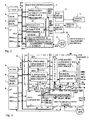
- Figure 2 shows the block diagram of the preferred pixel data conditioning circuitry by a print data controller.
- a first and a second printhead 1 and 2 are each connected via a driver unit (pen driver board) 11 and 12 to a print data controller 4, which at the input side receives 16 bits of parallel binary print image data from a bus 5 on the input side and serial on the output side binary print image data to the driver units 11 and 12 outputs.
- At least one microprocessor 6, a pixel memory 7, a nonvolatile memory 8 and a read-only memory 9 are connected in terms of address, data and control via the BUS 5.
- An encoder 3 is connected to the print data controller 4 to trigger the buffering of the binary pixel data and the printing of the print image columns, each printhead having a clock frequency of max.
- the print data controller 4 has a first and second pixel data processing unit 41 and 42 and the associated controls, such as DMA controller 43, address generator 44 and printer controller 45.
- the controllers include an evaluation unit 453 and a logic 452, which supplied the encoder pulses e for error reduction of printer errors become. It is provided that a printer controller 45 is connected to at least the DMA controller 43 and the address generator 44 and that the address generator 44 is connected to the pixel data processing unit 41, 42 in terms of control.
- the printer controller 45 is connected directly to the microprocessor 6 via the bus 5 and via an interrupt signal control line I.
- the DMA controller 43 is connected to the microprocessor 6 via a control line for DMA control signals DMA ACK , DMA REQ .
- FIG. 3 shows a section of the circuit arrangement according to FIG. 2 with the pixel data processing unit 42 for the second print head, with the DMA controller 43 for a direct memory access (DMA) as well as with the address generator 44 and the printer controller 45.
- the encoder 3 supplies a signal e and is connected to the inventive logic 452 of the printer controller 45.
- the latter is connected to the DMA controller 43 directly via control lines 46 for first DMA control signals (DMA start and DMA busy), the DMA controller 43 being supplied with the DMA start signal by the printer controller 45, and with the DMA Control 43 outputs the DMA busy signal with the value 'zero' to the printer controller 45 to signal that the DMA cycles have ended.
- the DMA controller 43 is also connected to the address generator 44 via a DMA busy signal control line 50.
- the printer controller 45 is connected to the microprocessor 6 via the bus 5 and via an interrupt signal control line 47, to the address generator 44 via a control line for supplying an address generator start signal AG-start and to the DMA controller 43 via a switching line 49 for a switching signal SO connected.
- At least the microprocessor 6, the pixel memory 7, the nonvolatile memory 8 and the read-only memory 9 are connected in terms of address, data and control via the bus 5. It is provided that the printer controller 45 has means for generating and outputting a switching signal SO in order to drive the pixel data processing unit 42 thereby selecting the pixel data from the respectively first or the respective second of the two latches 412 and 422 for transmission to the driver unit 12 become.
- the DMA controller 43 outputs the DMA-busy signal with the value 'Zero' to the printer controller 45 to signal that all direct memory accesses have occurred, i. the period is completed with DMA cycles.
- the printer controller 45 is connected to the address generator 44 via at least one control line for supplying a start signal (AG start).
- the address generator 44 has - in a manner not shown here - a unit for generating read addresses and means for forming an address read signal AR. If a number of address read signals AR has been generated for an address group A, the address generator 44 outputs a print start signal PS via the control line 48 to the printer controller 45.
- the printer controller 45 is connected to the microprocessor 6 via a control line 47 for an interrupt signal I and via the bus 5. At least the microprocessor 6, the pixel memory 7, the non-volatile memory 8 and read-only memory 9 are connected in terms of address, data and control via the BUS 5.
- the printer controller 45 has means for generating and outputting a switching signal SO and is connected via a control line to the DMA controller 43 and to the pixel data processing unit 42. The latter is driven to by means of Switching signal SO one of the latches 412, 422 for a transmission of pixel data to the driver unit 12 to select. The latter can thereby be supplied in groups to the binary pixel data of an already stored data string.
- the switching signal SO is supplied to the DMA controller 43 to select the other one of the latches 412 and 422 for pixel data loading.
- the DMA controller 43 has means for generating and outputting selection signals Sel_2.1, Sel_2.2 as a function of the switching state of the switching signal SO in order to buffer the binary pixel data into the respectively first or the respective second of the two latches 421 or 422, wherein in a transfer of pixel data from the respective one of the two latches to the driver unit 12, the respective other latches for buffering a data string are successively selected by the selection signals.
- the two pixel data processing units are each connected on the input side to the bus 5, but there only to the low-order 16 bits of the data bus.
- data word and “wordwise” should always be understood to mean a 16-bit wide data word if the data word width is not expressly specified additionally.
- the pixel data for a 1 ⁇ 2 inch printhead requires only half the space (at most 320 bits from each data string) in the pixel memory 7, from which this pixel data is provided to the pixel data conditioning unit 42.
- a data string for both printheads therefore requires that buffering of 20 * 16 bit data words each time be performed twice, for example in the respective first buffer.
- the first and second latches 421 and 422 are alternately selected by the selection signals Sel-2.1 and Sel-2.2.
- the DMA controller 43 is control connected to the microprocessor 6 and to the latches 421 and 422, that the DMA controller 43 comprises means for generating and outputting address write signals AW, which in a DMA access to the in Pixel memory 7 stored binary pixel data whose writing into the latches 421, 422 of the pixel data processing unit 42nd allow.
- the DMA controller 43 supplies a 5-bit address write signal AW for wordwise addressing. The latter is in each case at a separate address input of the first and second buffer memories 421 and 422 for pixel data for the second print head.
- the DMA controller 43 provides a first select signal Sel_2.1 for pixel data for the second printhead and asserts a separate control input of the first pixel data for the second printhead 421.
- the DMA controller 43 provides a second select signal Sel_2.2 for pixel data for the second printhead and asserts a separate control input of the second pixel data latch 422 for the second printhead.
- the address generator 44 has at least means for generating and outputting address signals AR, AP and control signals WR, LD, PS, and wherein the address signals AR, AP and control signals WR, LD of the pixel data processing unit 41, 42 for selecting the cached binary pixel data and their grouping in a predetermined order.
- Each pixel data processing unit has two latches, a selector for selecting the binary pixel data, and a shift register for parallel / serial conversion of the binary pixel data provided in a new order.
- the address read signals AR generated by the address generator 44 are supplied to the latches and the selector of the pixel data processing unit.
- the primitive address signals AP and the write control signal WR generated by the address generator 44 are supplied to the selector, and a load signal LD is supplied to the shift register. From the printer controller 45, a start signal AG-start is supplied to the address generator 44.
- the address generator 44 now provides an address read signal AR for selecting the data word with the pixel data destined for the second printhead.
- the higher-order bits of the address read signal AR are applied to a separate address input of the first and second buffer memories 421 and 422.
- the four least significant bits of the address read signal AR are applied to an address input of a second selector 423 and allow addressing within the 16-bit data word.
- the parallel data outputs of the first and second pixel data for the second printhead 421 and 422 are applied to a first and second input of the selector 423, controlled by the address generator 44 at its output a 14 bit parallel data signal to the parallel data input of a shift register 424 for Pixel data for the second printhead.
- the shift register 424 is controlled by a shift clock signal SCL of the printer controller 45, and outputs a serial data output signal SERIAL DATA OUT 2.
- the address generator 44 also generates a primitive address AP for controlling the selector 423 and a write signal WR.
- the address generator 44 outputs a load signal LD to the shift register 424 and a print start signal PS to the printer controller 45.
- the latter outputs the Latch and Print2 signals for the control of the Pen Driver Board 12.
- the printer controller 45 is connected via a control line for the output of the switching signal SO to a corresponding control input of the DMA controller 43 and to the selector 423 of the pixel data processing unit 42.
- the printer controller 45 has evaluation means for evaluating the address and control signals transmitted via BUS 5, which are evaluated with regard to the occurrence of a print command.
- the printer controller 45 generates at least the DMA start, AG start and SO signals, stores the latter in registers, and communicates with the DMA controller 43 via DMA start, DMA busy, and SO signal control lines.
- the SO signal is generated only upon receipt of a print command and triggered by the print command is output from the printer controller 45, a first control signal DMA start to the DMA controller 43, the latter then generates a request signal DMA REQ and sends to the microprocessor 6.
- the microprocessor has an internal DMA controller (not shown) which, in the case of a direct memory access, applies a specific address to the pixel memory (RAM) 7, thereby enabling word-wise transmission of binary pixel data via BUS 5 to the latches.
- An address write signal AW is supplied to the latches by the DMA controller 43 for this purpose.
- the microprocessor 6 can, for example, via DMA from the pixel memory 7 read out a 16-bit wide data word with pixel data and transmit it to the print data control unit.
- the microprocessor 6 sends an acknowledgment signal DMA ACK to the DMA controller 43 to synchronize the generation of the address write signal AW in the DMA controller 43 with the DMA cycle of the microprocessor 6.
- a 16-bit wide data word with binary pixel data enters a buffer.
- Each of the four latches can provide a total of 320 bits for further data conditioning after each 20 DMA cycles.
- DMA controller 43 supplies first and second select signals Sel_2.1 or Sel_2.2 alternately for word-wise storing pixel data for the second printhead.
- the DMA controller 43 supplies a first selection signal Sel_2.1 and an address write signal AW for the alternate and wordwise storage of pixel data for the second print head.
- the number of pixels desired for each print image column requires a maximum of 40 data words to buffer 16 bits in two out of four latches.
- circuit means are provided for outputting the second control signal DMA-busy and for realizing at least one cycle counter for a predetermined number of 16-bit data words.
- the binary pixel data for the first printhead is word-delivered via BUS 5 and applied to a corresponding data input of the first and second latches 411 and 412 for pixel data for the first printhead.
- the first pixel data processing unit 41 for the first printhead-not shown in detail- also includes first and second latches 411 and 412, which are each connected on the input side to the low-order 16 bits of the data bus of the bus 5.
- the address write signal supplied from the DMA controller 43 AW is also applied to each of a separate address input of the first and second latches 411 and 412 for pixel data for the first printhead.
- the DMA controller 43 supplies a first select signal Sel_1.1 for pixel data for the first printhead and asserts a separate control input of the first pixel data stager 411 for the first printhead.
- the DMA controller 43 provides a second select signal Sel_1.2 for pixel data for the first printhead and asserts a separate control input of the second pixel data for the first printhead.
- the address read signal AR provided by the address generator 44 is also applied again to a separate address input of the first and second buffer memories 411 and 412 for pixel data for the first print head and to a first selector 413.
- the parallel data outputs of the first and second pixel pixel data latches 411 and 412 are applied to first and second inputs of the selector 413, controlled by the address generator 44 at its output, a 14 bit parallel data signal to the parallel data input of a shift register 414 for Provides pixel data for the first printhead.
- the shift register 414 is controlled by the shift clock signal SCL of the printer controller 45 and outputs a serial data output signal Serial data out 1.
- the printer controller 45 outputs a shift clock SCL to the pixel data for the first printhead shift register 414 and signals Latch and Print1 for the control of the pen driver board 11.
- the printer controller 45 is connected to a corresponding control input of the DMA controller 43 and to the pixel data processing unit 41 via a control line for outputting the signal SO.
- the cycle counter of the DMA controller 43 is a word counter for a predetermined number of 16-bit data words, which is started by a DMA start signal.
- the DMA controller is for example part of an application specific circuit (ASIC), wherein the cycle counter is connected on the one hand to the aforementioned means for generating and output of address write signals AW and on the other hand with means for generating and outputting selection signals, the latter - In a manner not shown - have at least one output means and comparison means.
- a first comparison means controls the output means as a function of the SO signal in order to reach a first predetermined number of 16-bit data words for the first pixel data processing unit 41 specific selection signal Sel_1.1 or Sel_1.2 and after reaching the first predetermined number of 16-bit data words to output a for the second pixel data processing unit 42 specific selection signal Sel_2.1 or Sel_2.2.
- the first or second comparing means receives a signal which is applied to the cycle counter to terminate the counting of DMA cycles. From the signal, a DMA-busy signal with the value 'zero' is generated and output via a register.
- binary pixel data can be stored in the pixel memory in an optimal order, which relieves the microprocessor in the printed image change.
- Data transfer via DMA also relieves the load on the microprocessor.
- the error-reducing encoder pulses logic 542 is a component of the printer controller 45 and the associated evaluation unit (not shown) forms part of the address generator 44.
- the logic 542 then transmits a more than two-bit wide digital count signal ENC to the address generator 44 on the output side Comparator contains.
- a data string counter is further realized (not shown in detail), wherein each data string has a maximum of the above-mentioned number of 40 * 16-bit data words. After the binary pixel data taken from a data string has been printed, the data string counter is incremented when the LH edge of the encoder clock occurs. When a predetermined setpoint U on data strings is reached, printing of the print image is ended.
- the entire print data control can preferably be realized with an application specific circuit (ASIC) or programmable logic, such as Spartan II 2.5V FPGA from XILINX ( www.xilinx.com ).
- ASIC application specific circuit
- Spartan II 2.5V FPGA from XILINX ( www.xilinx.com ).
- FIG 4 shows a block diagram of the printer controller 45, which has a logic 542 for error reduction, which will be explained below with reference to FIG 6 in more detail.
- the aforementioned logic 542 is operatively connected to a sequencer and processing unit 451 to which a printer control logic 450 and an input / output unit 454 are connected.
- the first block 451 with the sequence control and processing unit are - not shown - an encoder filter and an encoder controller included, which provides a start signal for printing a column, an interrupt request with each rising edge of the encoder triggers and the correct time Transmission of print data within a print column supported.
- the encoder filter suppresses spikes on the encoder signals.
- the first block 451 - in a manner not shown - yet another counter and further evaluation circuits included, wherein the counter is a system clock for determining the period of encoder pulses is supplied.
- the e-input BUS-I / O and other registers of the I / O unit 454 communicate with the microprocessor.
- a microprocessor-controlled control of the pressure cycle duration causes - in a manner not shown - an adjustment of the printing cycle to a predetermined period of time, preferably about 90% of the time between two positive encoder edges.
- the input / output unit 454 also has a number of blocks - not shown in detail - but at least the following blocks, a BUS input / output unit 4541, an input signal 4542 for the encoder signal e, an input 4543 for the DMA busy signal, a DMA start signal register 4544, an AG busy signal input 4545, an AG start signal register 4546, a switching signal SO register 4547, a PS signal input 4550; Output 4551 for the I signal, an output 4553 for the shift-clock signal, an output 4554 for the latch pulse signal, a Print1 pulse output 4555 and a Print2 pulse output 455x.
- the input / output unit 454 has an ENC output 4560.
- the evaluation unit 453 shown in dashed lines is likewise a component of the printer controller 45, then the output signal of the evaluation unit 453 is likewise transmitted to the address generator 44, but only as a bit-wide binary abort signal that is present at the output 4560 is provided.
- the printer controller 45 can also be realized in the already explained or in an alternative embodiment, wherein each printer controller 45 - independent of the embodiment - has a data string counter 4503 and is connected to the encoder 3. After each printed data string, the value V of the data string counter is incremented when the encoder clock occurs, whereby the printing of the print image is terminated when a predetermined setpoint U of the data string counter is reached.
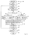
- FIG. 5 shows a flowchart for the flow control of the printer controller.
- a step 102 is reached and in the routine 100 of the sequence control, the signals reduction signal DEC_ENC, reset signal Encoderfarer_Reset and selection signals Sel_1.1, Sel_1.2, Sel_2.1, Sel_2.2 set to the value 'zero'.
- a data word transmitted via the bus is evaluated with regard to the occurrence of a command for printing start. If the latter has not yet been issued, then it branches into a waiting loop.
- the column count value V is set to the value 'zero'.
- the switching signal SO is set to the value 'one' and output.
- a second interrogation step 105 the encoder signal e is now evaluated with regard to the occurrence of an LH edge. If the latter has not yet occurred, a branch is made to a waiting loop.
- a signal DMA start is output and a subroutine 300 is started which sets certain selection signals Sel_1.1, Sel_1.2, Sel_2.1 or Sel_2.2 to the value 'one' in order to convert the binary pixel data into the Latch the pixel data processing units 41 and 42 to take over what will be explained in more detail later with reference to FIG.
- the encoder clock counter is incremented and the digital output signal ENC now becomes unlike the value 'zero'.
- a branch is thus made from the fourth interrogation step 109 in a step 110, in which the switching signal SO is logically negated and then output.
- step 111 the address generator is activated and a subroutine 400 is started, which generates for the pixel data processing units 41 and 42 specific read addresses AR and control signals such as the switching signal SO, the primitive address AP, the write signal WR and a load signal LD.
- step 112 a DMA start signal is output and DMA control is enabled to restart the aforementioned subroutine 300. Both subroutines 300 and 400 are in parallel with each other.
- the print cycle start is signalized by generating a short pulse or by setting the signal DEC_ENC to the value 'one' in a first substep 113a and the signal DEC_ENC to the value 'zero' in a second substep 113b.
- a fifth interrogation step 114 it is evaluated whether the address generator has finished its subroutine 400 and whether the DMA busy signal has been set to the value 'zero'. If the former or the latter is still not the case, then a branch is made in a waiting loop. However, if the address generator has completed its subroutine 400 and the DMA busy signal has been set to the value 'zero', then a step 115 is reached.
- a sixth interrogation step 116 it is evaluated whether the column count value V has reached a limit value U. If this is not the case, then the fourth query step 109 is branched back. Otherwise, the system branches back to the first interrogation step 103 via a step 117, and the routine restarts when a print start command is detected in the first interrogation step 103.
- a reset signal Encoderschreiber_Reset: 0 is generated and reset the encoder counter to the value 'zero'.
- FIG. 4 there is a separate second block 452 which is connected to the flow control and processing unit contained first block 451 of the printer controller 45 is operatively connected.
- the aforementioned block 452 contains the logic for printer error reduction and is part of the printer controller 45.
- the connection comprises a plurality of - not shown - lines for analog and / or digital electrical signals.
- the connection of the second block 452 to the ENC output of the I / O unit 454 is also via the first block 451 of the printer controller 45.
- the block 451 is connected to the I / O unit 454 of the printer controller 45. After powering up, the processing unit of the first block 451 sets the decrease signal DEC_ENC and the reset signal Encoder_counter_Reset to the value 'zero'.
- the printer controller 45 includes a third block 450 with the printer control logic. The latter has parameter Y in parameter memory 4505 as an upper limit for the printer error reduction logic.
- a separate second block may be omitted (not shown) if the printer error reduction logic is part of the first block 451 of the printer controller 45.
- FIG. 6 shows a block diagram of the logic for reducing printer errors.
- First and second AND gates 4521, 4522 are connected in output to the inputs of an encoder clock counter 4523, which has a first input CLK_down, a second input CLK_up, and a third input ENC_RESET for the reset signal Encoder Counter_Reset.
- the decrease signal DEC-ENC is supplied via a first input of the first AND gate 4521.
- the output K of a first digital comparator 4524 is connected.
- the first digital comparator 4524 used is an OR gate which combines the digital output signal ENC of the encoder clock counter 4523 and outputs a logic signal 'one' on the output side at ENC ⁇ 0.
- the filtered encoder signal e is supplied in series via a first input of the second AND gate 4522, to whose second input the output L of a second digital comparator 4525 is connected.
- the encoder clock counter 4523 is shown in the embodiment as a 4-bit counter, but should not be limited to this alone. Rather, embodiments other than n-bit counters are possible.
- both digital comparators are the same.
- n Exclusive OR gates are linked together on the output side via an OR gate, wherein each Exclusive OR gate compares one digit of the n-bit number with a corresponding position of the n-bit comparison number.
- the first digital comparator 4524 At the respective second inputs of the first digital comparator 4524 is an n-bit wide digital data signal with the binary value 'zero'. At the respective second inputs of the second digital comparator 4525 is an n-bit wide digital data signal with the corresponding binary values for an upper limit 'Y', which is supplied via the first block 451 of the printer controller 45.
- the first block 451 of the printer controller 45 also provides the encoder count_reset signal and the DEC ENC signal.
- the first digital comparator 4524 operates in a manner known per se and outputs a logic signal, for example TTL. For example, a binary value 'one' at the output K indicates that the condition ENC ⁇ 0 is fulfilled.
- the DEC-ENC signal supplied via a first input of the first AND gate 4521 is consequently switched through to the first input CLK_down of the encoder clock counter 4523 in order to decrement the count value.
- the second digital comparator 4525 outputs a logic signal having the binary value 'one' at the output L when the condition ENC ⁇ Y is satisfied.
- the filtered encoder signal e supplied via a first input of the second AND gate 4522 is then turned on to the second input CLK_up of the encoder clock counter 4523 to increment the count value.
- the first and second digital comparators 4524 and 4525 respectively provide a TTL signal with the Value 'zero' if the above condition is not met. In this case, the AND gates 4521 and 4522 are disabled.
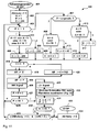
- FIG. 7 a shows a flowchart for reducing printer errors.
- the routine 700 is started in step 701. After the start, first in step 702 the count is reset to the value 'zero'. In the following interrogation step 703, in the expectation of an activation by means of a reset signal encoder counter reset with the value 'one', the process is continuously branched back to step 702.
- the reset signal encoder counter reset is set to the value 'one' after a first DMA cycle by the processing unit of the block 451 shown in FIG. 4, as can be seen from step 108 of FIG.
- the aforesaid reset signal is applied to the third input ENC_RESET of the encoder clock count 4523 shown in FIG. If an encoder count reset signal of value 'one' is detected in query step 703, then a second interrogation step 704 is reached in which it is determined whether an encoder LH edge is applied to the second AND gate 4522 via a first input while the second comparator 4525 outputs on the output side a value 'one', with which the latter signals that the condition ENC ⁇ Y is fulfilled.
- the second query step 704 branches to the third query step 706.
- the first comparator 4524 determines that the count ENC is not equal to the count value 'zero'. In this case, a branch is made to the fourth interrogation step 707. Otherwise it becomes the first query step 703 branches back.
- FIG. 7b shows a pulse / time diagram for the printer error reduction.
- the reset signal Encoder_outheastern_Reset and the decrease signal DEC_ENC are set to the value 'zero'.
- Several encoder pulses occur in too short a time interval over a longer period of time. In the pulse / time diagram of Figure 7b, however, the aforementioned period is longer than in the pulse / time diagram of Figure 1f.
- a first period begins at time t 0 to load the pixel data for the first print cycle into the latches via DMA cycles.
- a second encoder pulse occurs and the aforementioned encoder clock counter is incremented and now has the count value 'one'.
- the output K of the first comparator 4524 (FIG. 6) then outputs the binary value 'one' which is applied to the input of the first AND gate 4521.
- the output Q1 or K remain set to the binary value 'one' until the time t 3 .
- the incrementing is continued as long as a predetermined upper limit value Y is not reached, or the count value can be decremented upon the occurrence of a printing cycle.
- a second period is started with DMA cycles and a first print cycle for the pixel data of a data string loaded in the preceding first DMA period with DMA cycles.
- a pulse-shaped decrease signal DEC_ENC generated by the printer controller 45 is output to the logic 452, resulting in decrementing and the result that the count value again has the value 'zero'.
- the first-mentioned buffer of the print data controller 4 is read out for printing a data string.
- the pixel data for a second print cycle are loaded by DMA into the respective other buffer of the print data controller 4.
- a third encoder pulse already occurs before a third print cycle can be started.
- the outputs Q1 and K remain set to the binary value 'one' until time t 5 .
- a second print cycle and a third DMA period are started.
- the time interval of the subsequent times t 6 and t 7 , t 8 and t 9 and t 10 and t 11 increases to the extent that at time t 11 of the seventh encoder pulse before the sixth DMA period is effective.
- the encoder clock counter is no longer decremented to the same extent as it is incremented. As a result, the count increases.
- the first comparator 4524 checks the aforementioned logic 452 as to whether the counter contents are nonzero. If this is the case, it is waited for a reduction signal DEC_ENC.
- the printer controller outputs a decrease signal DEC_ENC.
- the encoder clock counter is still incremented before decrementing.
- the outputs Q1 and K remain set to the binary value 'one' from time t 10 to time t 11 and then change to the value 'zero'.
- the output Q2 changes to the binary value 'one', ie the counter content has risen to the count value 'two' at time t 11 .
- This counter state stops only until the time t 12 , since at the time t 11 , a reduction signal DEC_ENC with the value 'one' to the encoder clock counter was delivered.
- Output Q2 returns to binary 'zero' and output Q1 returns to binary 'one' according to the decremented 'one' count.
- the eighth encoder pulse is output and there are comparable conditions as at time t 2 with the exception that the encoder clock count before incrementing is now at the aforementioned value 'one'.
- the eighth encoder pulse at time t 13 is effective before the seventh DMA period with DMA cycles.
- Output Q2 returns to binary 'one' and output Q1 returns to binary 'zero' according to the incremented count 'two'.
- This counter state stops only until the time t 14 , since at the time t 13 also a decrementing signal DEC_ENC with the value 'one' was delivered to the encoder clock counter.
- FIG. 8 shows a block diagram of an embodiment of the address generator.
- the address generator 44 has an input / output logic 444, an evaluation unit 442 and a read address generation unit 441, the latter having a first counter 4410 for the primitive address and an associated first comparator 4411 for comparing a count value P of the primitive address with a first setpoint supplied by a first setpoint register 4412.
- the unit 441 comprises a second counter 4413 for an address group and an associated second comparator 4414 for comparing a count A of the address group with a second set value supplied by a second setpoint register 4415 and a scheduler 4401.
- the latter works in conjunction with a calculation unit 4402 for the parameter C, a WR signal generator 4403, an LD signal generator 4404, a PS signal generator 4405, with the aforementioned counters 4410 and 4413, with the comparators 4411, 4414, 4418, with the registers 4412, 4415 4417 and with a AGbusy signaling device 4416.
- the evaluation unit 442 includes an inverter 4420 for the DMA busy signal, an AND gate 4423, a register 4422 for at least a third setpoint value Z and a third comparator 4421, the count value the encoder clock counter for comparison with at least one third setpoint Z is supplied.
- the third comparator 4421 may be simply constructed by checking that neither ENC values are 'zero' nor 'one'. occur.
- the logic signals output at the Q outputs of the encoder clock counter are linked via an OR gate and on the other hand n Exclusive OR gates on the output side via a second OR gate, whereby each Exclusive OR gate in each case has one position of the n-gate.
- the AND gate 4423 outputs an abort signal BO having the value 'one' on the output side when the negated DMA busy signal and the output signal of the third comparator 4421 have the value 'one'.
- the input / output logic 444 of the address generator 44 has an input 4450 for the DMA busy signal, an input 4451 for the ENC signal, an input 4444 for receiving the address generator start signal and a register 4445 for the signal to be sent Addressgeneratorbusysignal comprises.
- the printer controller may already include the above-mentioned comparison of the ENC signal with the setpoint value Z, in order to generate an abort signal BO as a result of the comparison.
- the I / O unit 454 of the printer controller 45 then includes a BO output instead of the ENC output 4560.
- the input / output logic 444 of the address generator 44 need only contain a BO input instead of the ENC input 4451 which has the abort signal BO instead of the count ENC is supplied. This eliminates the control line 50, the DMA busy input 4450 and the evaluation 442 in the address generator 44.
- a corresponding evaluation unit 453 is instead realized in the printer controller 45 to perform the above comparison of the ENC signal with the setpoint Z and the result the comparison to generate an abort signal for the printing cycle that is supplied to the address generator 44.
- the address generator 44 After a formation of the address read signal AR and after an incrementation of a count value P for the primitive address by the value 'one', the comparison is made in the first comparator 4411, wherein after successively generates a number of read addresses, exceeding the first setpoint or an overflow of the Counter 4410 for the primitive address is triggered, a load signal LD is output and a subroutine for output is started, the counter 4413 for an address group is incremented by the value 'one', wherein falling below the second setpoint in the comparison in the second comparator 4414, a reset of the count value P of the primitive address to the value 'one' and generating a subsequent read address associated with a further address group and wherein upon the occurrence of a predetermined condition, a running print cycle is aborted prematurely.
- the process controller 4401 is provided with a parameter C calculating unit 4402 having a signal generator 4403 for generating a write signal WR, a signal generator 4404 for generating a load signal LD, and another signal generator 4405 for generating a print start signal PS for causing the pixel data to be printed out Data string and connected to the Busy signal generator 4416.
- the input / output logic 444 also has a register 4446 for the delivery of the primitive address AP, a register 4447 for the write signal WR, a register 4448 for the load signal LD, a register 4449 for the output of the address read signal AR and a register 4440 for the output of the Pressure start signal PS on.
- FIG. 9 shows a block diagram of a DMA controller.
- the DMA controller 43 has at least one scheduler 4301, a word counter 4302, a setpoint register 4303, an input / output logic 4304, a memory 4305, a comparator 4306, and a shift register 4307, which are interconnected to perform DMA cycles.
- Integrated into the flow control 4301 is a further processing unit to which the aforementioned blocks 4302 to 4307 are connected in circuit and which has further comparators (not shown).
- the input / output logic 4304 at least one input 43042 for the received DMA start signal and Registers 43043 to 43046 for the select signals to be transmitted, a DMA busy signal register 43047, a request signal DMA REQ register 43048, an input acknowledgment signal DMA ACK input 43049, an input 43050 for the switching signal (SO) and register 43051 for the address write signal AW.
- FIG. 10 shows a flowchart for DMA control.
- a subroutine 300 is called when a DMA start signal is output from the printer controller 45 to the DMA controller 43 (step 301).
- a word count W is set to the value 'zero'.
- a DMA-busy signal is set to the value 'one' and transmitted to the printer controller 45.
- a DMA request signal DMA REQ having a value 'zero' is transmitted to the microprocessor 6. The latter transmits an acknowledgment signal DMA ACK to the DMA controller 43.
- a non-receipt of the acknowledgment signal DMA ACK branches to a waiting loop with a value 'zero'.
- a second interrogation step 305 is skipped, wherein the state of the switching signal SO is determined. If the switching signal SO has the state equal to one, then a branch is made to a third interrogation step 306. Otherwise, the switching signal SO has the state equal to 'zero' and a branch is made to a fourth interrogation step 309.
- step 306 it is checked whether the word counter has a value W smaller than twenty. For this case (W ⁇ 20), a branch is made to a step 307.
- step 307 the first selection signal for the first print head Sel_1.1. switched to the value 'one' and the address write signal AW receives the current value W of the word counter.
- step 312 the pixel data are transferred to the latches of the pixel data modification units 41, 42.
- step 313 all selection signals are switched to the value 'zero' and a DMA request signal DMA REQ with a value 'one' is transmitted to the microprocessor 6.
- step 314 the word count W is incremented with the value 'one'.
- a subsequent query step 315 it is checked whether the word counter has a value W less than forty. For this case, in which the word counter has such a value W ⁇ 40, a branch back to a step 303. Otherwise, a branch is made to a step 316 to output a signal DMA busy having the value 'zero' before the end (step 317) of the subroutine 300 is reached. Otherwise, if it is determined in the third query step 306 that the word count W is not less than twenty, then a branch is made to a step 308 in which the first selection signal for the second print head Sel_2.1. is switched to the value 'one' and the address write signal AW is replaced by the value 'twenty' reduced current value W of the word counter. In the subsequent step 312, the pixel data are taken back into the buffer.
- step 309 it is also checked whether the word counter has the predetermined value W ⁇ 20, it being previously determined in the interrogation step 305 that the binary switching signal SO does not have the value equal to one. If the word counter has the predetermined value W ⁇ 20, then in step 310, the second selection signal for the first printhead Sel_1.2. switched to the value 'one' and the address write signal AW receives the current value W of the word counter. In the subsequent step 312, the pixel data are taken back into the buffer.
- the fourth interrogation step 309 branches to a step 311 in which the second selection signal for the second printhead Sel_2.2 is switched to the value 'one' and the address write signal AW the by the value 'Twenty' reduced actual value W of the word counter receives.
- the pixel data are taken back into the buffer.
- FIG. 11 shows a flowchart for address generation.
- the addresses of stored binary pixel data begin at both printheads with the start address zero, which is generated in the following manner for the address read signal AR.
- the first query step 403 it is asked if the numerical value P of the counter of the primitive address is equal to the value one. If so, the second query step 404 is reached. Here it is determined whether the counter A has reached the value 8 or 9 or 15 or 16.
- step 406 is executed and the numerical value C is subtracted from the numerical value C of the counter of the address read signal AR.
- the numerical value C of the counter of the address read signal AR is greater than or equal to the value zero and then branches to step 419 for the output of the address read signal AR. Otherwise, a branch is made to step 420 in order to add a numerical value 512 to the negative numerical value. After steps 419 and 420, steps 425, 426 and 427 are traversed.
- step 425 the numerical value for the counter of the primitive address AP is output.
- step 426 a write signal WR for the binary pixel data entry is output to a collection register.
- step 427 the numerical value for the numerator of the primitive address AP is incremented by the value one.
- a fourth interrogation step 428 is reached and it is determined that the numerical value P of the counter of the primitive address AP has not yet reached the limit value 15. Subsequently, branching back to the first query step 403.
- the program branches to the sixth query step 408, in which it is checked whether the counter of the address group has the value 8 or 15. If this is the case, then a branch is made to a step 409 and the numerical value 3 is added to the numerical value C of the counter of the address read signal AR. Otherwise, branching is made from the sixth interrogation step 408 to a step 410, and the numerical value 47 is added to the numerical value C of the counter of the address read signal AR.
- the fifth query step 407 branches to the seventh query step 415, in which it is checked whether the counter of the address group has the value 8 or 15. If this is the case, then a branch is made to a step 416 and the numerical value 41 is added to the numerical value C of the counter of the address read signal AR. Otherwise, a branch is made from the seventh interrogation step 415 to a step 417 and the numerical value C is subtracted from the numerical value C of the counter of the address read signal AR.
- the third interrogation step 418 is reached again and it is determined whether the numerical value C of the counter of the address read signal AR is greater than or equal to the value zero.
- steps 419 and 420 steps 425, 426 and 427 are again run until the fourth interrogation step 428 is reached, in which it is determined whether the numerical value P of the counter of the primitive address AP has already reached the limit value 15. If this is the case, then a branch is made to a step 429 and a charging signal for loading the shift register is output.
- a subroutine 500 is started in step 430, in which inter alia a shift clock signal SCL is applied the shift register is applied to serially output the pixel data from the latter.
- step 431 the value of the counter of the address group is incremented by the value one.
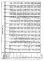
- FIG. 12 shows a table for generating addresses, whose address read signals AR for 22 address groups are generated by the aforementioned routine 400.
- the address generator 44 preferably generates the address values as a binary number and applies them to the pixel data processing units 41, 42.
- a binary number may be represented as a hexadecimal number or a decimal number, which requires less space. Only for this reason and for better understanding are decimal numbers entered in the table.
- the address read signal AR (address read) is thus generated for 14 binary numbers per address group. One after the other corresponding binary numbers are generated as address read signal AR for 22 address groups.
- Each address read signal AR is accessed in the buffer memory for a binary pixel
- the address values greater than 500 must therefore not be able to be generated completely as a binary number.
- all address values greater than 299 are generated but also not needed for printing.
- Routine 400 is executed until all print image columns have been printed or aborted. It has already been explained that the rows of nozzles of a printhead become active alternately for printing image columns. While one of the latches is being loaded with binary pixel data via direct memory access, the other latches are read out to transfer rendered groups of binary pixel data to the driver units. The mutual repetition of the routine 400 and further subsequent steps are caused by the printer controller 45, which under the control of a signal e of the encoder 3 also generates the print signals Print 1 or Print 2.
- FIG. 13 shows a flowchart of the output routine 500.
- the address generator 44 outputs a print start signal PS to the printer controller 45.
- the issue routine is called twenty-two times as a subroutine in the course of subroutine 400 to drive the shift registers in the print data controller 41, 42 and around the driver units 11, 12.
- a step 502 is reached and a shift clock SCL is generated in order to shift the pixel data loaded in the shift register via the serial data output to the respective drive unit 11, 12.
- step 503 a latch signal is generated and output to the driver units 11, 12.
- the print signals Print1, Print2 are generated and output to the driver units 11, 12 and in step 505 the subroutine 500 is stopped.
- each data string exists a first and second number of data words, respectively, containing binary pixel data for a first and a second inkjet printhead 1, 2, respectively.
- Each inkjet printhead 1, 2 prints one-half of each print image column, with odd-numbered pixels on at least one half of a first print image column and even-numbered pixels on at least one half through the first and second nozzle rows of each inkjet printhead a second printed image column to be printed.
- the first or second number of data words in the data string respectively contain the binary pixel data for both nozzle rows of the first and second inkjet printhead, wherein in each data word of each data string only the first and second pixel data are contained for printing a first or further print image column, so that one of the print image columns is completely printed only after printing out the pixel data, for example, three data strings or at least one further data string.
- the row of nozzles respectively in the transport direction in the first direction is supplied with the binary pixel data for the odd-numbered pixels of the first print image column, while the nozzle row in the transport direction in the second direction is already supplied with the binary pixel data for the even-numbered pixels the subsequent further print image column is supplied.
- Each print image column half is printed by the first and second nozzle rows of each ink jet print head, each print image column half being completed in time after printing with the second nozzle row by printing with the respective first nozzle row.
Landscapes
- Engineering & Computer Science (AREA)
- Computer Security & Cryptography (AREA)
- Physics & Mathematics (AREA)
- General Physics & Mathematics (AREA)
- Record Information Processing For Printing (AREA)
- Accessory Devices And Overall Control Thereof (AREA)
- Sorting Of Articles (AREA)
- Devices For Checking Fares Or Tickets At Control Points (AREA)
- Dot-Matrix Printers And Others (AREA)
- Electronic Switches (AREA)
- Handling Of Sheets (AREA)
Priority Applications (4)
| Application Number | Priority Date | Filing Date | Title |
|---|---|---|---|
| DE50301430T DE50301430D1 (de) | 2003-06-27 | 2003-06-27 | Verfahren und Anordnung zur Reduzierung von Druckerfehlen während des Drukens in einem Postbearbeitungsgerät |
| DK03090193T DK1491347T3 (da) | 2003-06-27 | 2003-06-27 | Fremgangsmåde og anordning til reduktion af trykfejl i et postbearbejdningsapparat |
| EP03090193A EP1491347B1 (fr) | 2003-06-27 | 2003-06-27 | Méthode et système pour réduire les erreurs d'impression dans un appareil de traitement de courrier |
| AT03090193T ATE307032T1 (de) | 2003-06-27 | 2003-06-27 | Verfahren und anordnung zur reduzierung von druckerfehlen während des drukens in einem postbearbeitungsgerät |
Applications Claiming Priority (1)
| Application Number | Priority Date | Filing Date | Title |
|---|---|---|---|
| EP03090193A EP1491347B1 (fr) | 2003-06-27 | 2003-06-27 | Méthode et système pour réduire les erreurs d'impression dans un appareil de traitement de courrier |
Publications (2)
| Publication Number | Publication Date |
|---|---|
| EP1491347A1 true EP1491347A1 (fr) | 2004-12-29 |
| EP1491347B1 EP1491347B1 (fr) | 2005-10-19 |
Family
ID=33395932
Family Applications (1)
| Application Number | Title | Priority Date | Filing Date |
|---|---|---|---|
| EP03090193A Expired - Lifetime EP1491347B1 (fr) | 2003-06-27 | 2003-06-27 | Méthode et système pour réduire les erreurs d'impression dans un appareil de traitement de courrier |
Country Status (4)
| Country | Link |
|---|---|
| EP (1) | EP1491347B1 (fr) |
| AT (1) | ATE307032T1 (fr) |
| DE (1) | DE50301430D1 (fr) |
| DK (1) | DK1491347T3 (fr) |
Citations (9)
| Publication number | Priority date | Publication date | Assignee | Title |
|---|---|---|---|---|
| US5337248A (en) * | 1992-02-25 | 1994-08-09 | Pitney Bowes Inc. | Mailing machine including sheet feeding speed calibrating means |
| DE29716523U1 (de) * | 1997-09-05 | 1997-11-20 | Francotyp-Postalia AG & Co., 16547 Birkenwerder | Frankiermaschine |
| US5912979A (en) * | 1990-11-02 | 1999-06-15 | Bell & Howell Mail Processing Systems Co. | Method and apparatus for object surveillance along a transport path |
| US20020003565A1 (en) * | 2000-07-06 | 2002-01-10 | Inten Wolfgang Von | Device for printing a print carrier |
| EP1176016A2 (fr) | 2000-07-26 | 2002-01-30 | Francotyp-Postalia Aktiengesellschaft & Co. | Dispositif et méthode d'adaptation automatisée des cycles de chauffage des têtes d'impression jet d'encre |
| DE10060454A1 (de) * | 2000-11-28 | 2002-05-29 | Francotyp Postalia Gmbh | Anordnung für eine Druckvorrichtung |
| US6457901B1 (en) | 2000-09-01 | 2002-10-01 | Precision Cover Systems, Inc. | Adjustable manhole apparatus |
| DE10230679A1 (de) | 2002-07-04 | 2004-01-22 | Francotyp-Postalia Ag & Co. Kg | Verfahren zum Steuern des Druckens in einem Postbearbeitungsgerät |
| DE10230678A1 (de) | 2002-07-04 | 2004-03-25 | Francotyp-Postalia Ag & Co. Kg | Anordnung zum Steuern des Druckens in einem Postbearbeitungsgerät |
-
2003
- 2003-06-27 AT AT03090193T patent/ATE307032T1/de active
- 2003-06-27 DE DE50301430T patent/DE50301430D1/de not_active Expired - Lifetime
- 2003-06-27 EP EP03090193A patent/EP1491347B1/fr not_active Expired - Lifetime
- 2003-06-27 DK DK03090193T patent/DK1491347T3/da active
Patent Citations (9)
| Publication number | Priority date | Publication date | Assignee | Title |
|---|---|---|---|---|
| US5912979A (en) * | 1990-11-02 | 1999-06-15 | Bell & Howell Mail Processing Systems Co. | Method and apparatus for object surveillance along a transport path |
| US5337248A (en) * | 1992-02-25 | 1994-08-09 | Pitney Bowes Inc. | Mailing machine including sheet feeding speed calibrating means |
| DE29716523U1 (de) * | 1997-09-05 | 1997-11-20 | Francotyp-Postalia AG & Co., 16547 Birkenwerder | Frankiermaschine |
| US20020003565A1 (en) * | 2000-07-06 | 2002-01-10 | Inten Wolfgang Von | Device for printing a print carrier |
| EP1176016A2 (fr) | 2000-07-26 | 2002-01-30 | Francotyp-Postalia Aktiengesellschaft & Co. | Dispositif et méthode d'adaptation automatisée des cycles de chauffage des têtes d'impression jet d'encre |
| US6457901B1 (en) | 2000-09-01 | 2002-10-01 | Precision Cover Systems, Inc. | Adjustable manhole apparatus |
| DE10060454A1 (de) * | 2000-11-28 | 2002-05-29 | Francotyp Postalia Gmbh | Anordnung für eine Druckvorrichtung |
| DE10230679A1 (de) | 2002-07-04 | 2004-01-22 | Francotyp-Postalia Ag & Co. Kg | Verfahren zum Steuern des Druckens in einem Postbearbeitungsgerät |
| DE10230678A1 (de) | 2002-07-04 | 2004-03-25 | Francotyp-Postalia Ag & Co. Kg | Anordnung zum Steuern des Druckens in einem Postbearbeitungsgerät |
Also Published As
| Publication number | Publication date |
|---|---|
| EP1491347B1 (fr) | 2005-10-19 |
| DK1491347T3 (da) | 2006-03-06 |
| DE50301430D1 (de) | 2006-03-02 |
| ATE307032T1 (de) | 2005-11-15 |
Similar Documents
| Publication | Publication Date | Title |
|---|---|---|
| DE102005007220B4 (de) | Verfahren und Anordnung zum Steuern des Druckens eines Thermotransferdruckgeräts | |
| DE4445053C2 (de) | Frankiermaschineninterne Schnittstellenschaltung | |
| DE3236297A1 (de) | Tintenstrahldruckvorrichtung | |
| EP1416430B1 (fr) | Dispositif pour imprimer des images ayant des zones d'impression à résolutions différentes | |
| DE3836310C2 (de) | Verfahren zum Einstellen einer Wendeeinrichtung an einer Druckmaschine mit mehreren Druckwerken | |
| DE2605821A1 (de) | Schnelldrucker | |
| DE1524442A1 (de) | Regelvorrichtung fuer die Anzahl der Formularzeilenvorschuebe pro Zeiteinheit an einem Kettendrucker | |
| DE1817804C3 (fr) | ||
| EP1378820B1 (fr) | Système de contrôle d'imprimante dans un système de traitement de courrier | |
| DE2156599B2 (de) | Steuersystem fur Hochleistungsschnelldruckmaschinen | |
| EP1387245B1 (fr) | Méthode de contrôle d'une imprimante dans un système de traitement de courrier | |
| DE102010017004B4 (de) | Bearbeitungseinrichtung und Verfahren zum Ansteuern einer Bearbeitungseinrichtung | |
| DE2331928B2 (de) | Druckvorrichtung zum ausdrucken von daten in einer tabelle | |
| DE1940703C3 (de) | Einrichtung zum steuerbaren Vorschub einer Papierbahn in einem Drucker | |
| DE2940019C2 (fr) | ||
| DE69729677T2 (de) | Druckgerät und Verfahren zu seiner Steuerung | |
| DE3400712C2 (fr) | ||
| EP1491347B1 (fr) | Méthode et système pour réduire les erreurs d'impression dans un appareil de traitement de courrier | |
| DE2633155B2 (de) | Einrichtung zur Erzeugung zeitdefinierter Funktionssteuersignale | |
| DE2236662B2 (de) | Elektronisch gesteuertes Hammerdruckwerk | |
| DE2057675A1 (de) | Steuergeraet fuer den Druckhammerantrieb | |
| DE1920199A1 (de) | Mechanischer Schnelldrucker | |
| DE2909826B2 (de) | Elektronische Registrierkasse | |
| DE2416211C3 (de) | Elektronische Steuereinrichtung fur die Druckgeschwindigkeit eines Hochleistungs-Punktschriftdruckers | |
| DE2115141C3 (de) | Vorrichtung zum Drucken von kontinuierlich nacheinander empfangenen Daten |
Legal Events
| Date | Code | Title | Description |
|---|---|---|---|
| PUAI | Public reference made under article 153(3) epc to a published international application that has entered the european phase |
Free format text: ORIGINAL CODE: 0009012 |
|
| 17P | Request for examination filed |
Effective date: 20031218 |
|
| AK | Designated contracting states |
Kind code of ref document: A1 Designated state(s): AT BE BG CH CY CZ DE DK EE ES FI FR GB GR HU IE IT LI LU MC NL PT RO SE SI SK TR |
|
| AX | Request for extension of the european patent |
Extension state: AL LT LV MK |
|
| GRAP | Despatch of communication of intention to grant a patent |
Free format text: ORIGINAL CODE: EPIDOSNIGR1 |
|
| GRAS | Grant fee paid |
Free format text: ORIGINAL CODE: EPIDOSNIGR3 |
|
| GRAA | (expected) grant |
Free format text: ORIGINAL CODE: 0009210 |
|
| AKX | Designation fees paid |
Designated state(s): AT BE BG CH CY CZ DE DK EE ES FI FR GB GR HU IE IT LI LU MC NL PT RO SE SI SK TR |
|
| AK | Designated contracting states |
Kind code of ref document: B1 Designated state(s): AT BE BG CH CY CZ DE DK EE ES FI FR GB GR HU IE IT LI LU MC NL PT RO SE SI SK TR |
|
| PG25 | Lapsed in a contracting state [announced via postgrant information from national office to epo] |
Ref country code: RO Free format text: LAPSE BECAUSE OF FAILURE TO SUBMIT A TRANSLATION OF THE DESCRIPTION OR TO PAY THE FEE WITHIN THE PRESCRIBED TIME-LIMIT Effective date: 20051019 Ref country code: CZ Free format text: LAPSE BECAUSE OF FAILURE TO SUBMIT A TRANSLATION OF THE DESCRIPTION OR TO PAY THE FEE WITHIN THE PRESCRIBED TIME-LIMIT Effective date: 20051019 Ref country code: IE Free format text: LAPSE BECAUSE OF FAILURE TO SUBMIT A TRANSLATION OF THE DESCRIPTION OR TO PAY THE FEE WITHIN THE PRESCRIBED TIME-LIMIT Effective date: 20051019 Ref country code: FI Free format text: LAPSE BECAUSE OF FAILURE TO SUBMIT A TRANSLATION OF THE DESCRIPTION OR TO PAY THE FEE WITHIN THE PRESCRIBED TIME-LIMIT Effective date: 20051019 Ref country code: SK Free format text: LAPSE BECAUSE OF FAILURE TO SUBMIT A TRANSLATION OF THE DESCRIPTION OR TO PAY THE FEE WITHIN THE PRESCRIBED TIME-LIMIT Effective date: 20051019 Ref country code: SI Free format text: LAPSE BECAUSE OF FAILURE TO SUBMIT A TRANSLATION OF THE DESCRIPTION OR TO PAY THE FEE WITHIN THE PRESCRIBED TIME-LIMIT Effective date: 20051019 |
|
| REG | Reference to a national code |
Ref country code: GB Ref legal event code: FG4D Free format text: NOT ENGLISH |
|
| REG | Reference to a national code |
Ref country code: CH Ref legal event code: EP |
|
| REG | Reference to a national code |
Ref country code: IE Ref legal event code: FG4D Free format text: LANGUAGE OF EP DOCUMENT: GERMAN |
|
| REG | Reference to a national code |
Ref country code: CH Ref legal event code: NV Representative=s name: ROTTMANN, ZIMMERMANN + PARTNER AG |
|
| RAP2 | Party data changed (patent owner data changed or rights of a patent transferred) |
Owner name: FRANCOTYP-POSTALIA GMBH |
|
| PG25 | Lapsed in a contracting state [announced via postgrant information from national office to epo] |
Ref country code: SE Free format text: LAPSE BECAUSE OF FAILURE TO SUBMIT A TRANSLATION OF THE DESCRIPTION OR TO PAY THE FEE WITHIN THE PRESCRIBED TIME-LIMIT Effective date: 20060119 Ref country code: GR Free format text: LAPSE BECAUSE OF FAILURE TO SUBMIT A TRANSLATION OF THE DESCRIPTION OR TO PAY THE FEE WITHIN THE PRESCRIBED TIME-LIMIT Effective date: 20060119 Ref country code: BG Free format text: LAPSE BECAUSE OF FAILURE TO SUBMIT A TRANSLATION OF THE DESCRIPTION OR TO PAY THE FEE WITHIN THE PRESCRIBED TIME-LIMIT Effective date: 20060119 |
|
| PG25 | Lapsed in a contracting state [announced via postgrant information from national office to epo] |
Ref country code: ES Free format text: LAPSE BECAUSE OF FAILURE TO SUBMIT A TRANSLATION OF THE DESCRIPTION OR TO PAY THE FEE WITHIN THE PRESCRIBED TIME-LIMIT Effective date: 20060130 |
|
| GBT | Gb: translation of ep patent filed (gb section 77(6)(a)/1977) |
Effective date: 20060130 |
|
| NLT2 | Nl: modifications (of names), taken from the european patent patent bulletin |
Owner name: FRANCOTYP-POSTALIA GMBH Effective date: 20060104 |
|
| REF | Corresponds to: |
Ref document number: 50301430 Country of ref document: DE Date of ref document: 20060302 Kind code of ref document: P |
|
| REG | Reference to a national code |
Ref country code: DK Ref legal event code: T3 |
|
| PG25 | Lapsed in a contracting state [announced via postgrant information from national office to epo] |
Ref country code: PT Free format text: LAPSE BECAUSE OF FAILURE TO SUBMIT A TRANSLATION OF THE DESCRIPTION OR TO PAY THE FEE WITHIN THE PRESCRIBED TIME-LIMIT Effective date: 20060320 |
|
| PG25 | Lapsed in a contracting state [announced via postgrant information from national office to epo] |
Ref country code: HU Free format text: LAPSE BECAUSE OF FAILURE TO SUBMIT A TRANSLATION OF THE DESCRIPTION OR TO PAY THE FEE WITHIN THE PRESCRIBED TIME-LIMIT Effective date: 20060420 |
|
| REG | Reference to a national code |
Ref country code: IE Ref legal event code: FD4D |
|
| PG25 | Lapsed in a contracting state [announced via postgrant information from national office to epo] |
Ref country code: MC Free format text: LAPSE BECAUSE OF NON-PAYMENT OF DUE FEES Effective date: 20060630 Ref country code: BE Free format text: LAPSE BECAUSE OF NON-PAYMENT OF DUE FEES Effective date: 20060630 |
|
| ET | Fr: translation filed | ||
| PLBE | No opposition filed within time limit |
Free format text: ORIGINAL CODE: 0009261 |
|
| STAA | Information on the status of an ep patent application or granted ep patent |
Free format text: STATUS: NO OPPOSITION FILED WITHIN TIME LIMIT |
|
| 26N | No opposition filed |
Effective date: 20060720 |
|
| BERE | Be: lapsed |
Owner name: FRANCOTYP-POSTALIA A.G. & CO. KG Effective date: 20060630 |
|
| PG25 | Lapsed in a contracting state [announced via postgrant information from national office to epo] |
Ref country code: EE Free format text: LAPSE BECAUSE OF FAILURE TO SUBMIT A TRANSLATION OF THE DESCRIPTION OR TO PAY THE FEE WITHIN THE PRESCRIBED TIME-LIMIT Effective date: 20051019 |
|
| PG25 | Lapsed in a contracting state [announced via postgrant information from national office to epo] |
Ref country code: LU Free format text: LAPSE BECAUSE OF NON-PAYMENT OF DUE FEES Effective date: 20060627 Ref country code: TR Free format text: LAPSE BECAUSE OF FAILURE TO SUBMIT A TRANSLATION OF THE DESCRIPTION OR TO PAY THE FEE WITHIN THE PRESCRIBED TIME-LIMIT Effective date: 20051019 |
|
| PG25 | Lapsed in a contracting state [announced via postgrant information from national office to epo] |
Ref country code: CY Free format text: LAPSE BECAUSE OF FAILURE TO SUBMIT A TRANSLATION OF THE DESCRIPTION OR TO PAY THE FEE WITHIN THE PRESCRIBED TIME-LIMIT Effective date: 20051019 |
|
| REG | Reference to a national code |
Ref country code: CH Ref legal event code: PFA Owner name: FRANCOTYP-POSTALIA GMBH Free format text: FRANCOTYP-POSTALIA GMBH#TRIFTWEG 21-26#16547 BIRKENWERDER (DE) -TRANSFER TO- FRANCOTYP-POSTALIA GMBH#TRIFTWEG 21-26#16547 BIRKENWERDER (DE) |
|
| REG | Reference to a national code |
Ref country code: DE Ref legal event code: R084 Ref document number: 50301430 Country of ref document: DE |
|
| REG | Reference to a national code |
Ref country code: GB Ref legal event code: 746 Effective date: 20130319 |
|
| REG | Reference to a national code |
Ref country code: DE Ref legal event code: R081 Ref document number: 50301430 Country of ref document: DE Owner name: FRANCOTYP-POSTALIA GMBH, DE Free format text: FORMER OWNER: FRANCOTYP-POSTALIA AG & CO. KG, 16547 BIRKENWERDER, DE Effective date: 20130319 Ref country code: DE Ref legal event code: R084 Ref document number: 50301430 Country of ref document: DE Effective date: 20130314 |
|
| REG | Reference to a national code |
Ref country code: GB Ref legal event code: 732E Free format text: REGISTERED BETWEEN 20130516 AND 20130522 |
|
| REG | Reference to a national code |
Ref country code: GB Ref legal event code: 732E Free format text: REGISTERED BETWEEN 20130523 AND 20130529 |
|
| REG | Reference to a national code |
Ref country code: DE Ref legal event code: R081 Ref document number: 50301430 Country of ref document: DE Owner name: FRANCOTYP-POSTALIA GMBH, DE Free format text: FORMER OWNER: FRANCOTYP-POSTALIA GMBH, 16547 BIRKENWERDER, DE Effective date: 20150330 |
|
| REG | Reference to a national code |
Ref country code: FR Ref legal event code: PLFP Year of fee payment: 14 |
|
| REG | Reference to a national code |
Ref country code: CH Ref legal event code: PCAR Free format text: NEW ADDRESS: GARTENSTRASSE 28 A, 5400 BADEN (CH) |
|
| REG | Reference to a national code |
Ref country code: FR Ref legal event code: PLFP Year of fee payment: 15 |
|
| REG | Reference to a national code |
Ref country code: FR Ref legal event code: PLFP Year of fee payment: 16 |
|
| PGFP | Annual fee paid to national office [announced via postgrant information from national office to epo] |
Ref country code: NL Payment date: 20220620 Year of fee payment: 20 Ref country code: IT Payment date: 20220627 Year of fee payment: 20 Ref country code: GB Payment date: 20220627 Year of fee payment: 20 Ref country code: DK Payment date: 20220622 Year of fee payment: 20 Ref country code: DE Payment date: 20220510 Year of fee payment: 20 |
|
| PGFP | Annual fee paid to national office [announced via postgrant information from national office to epo] |
Ref country code: AT Payment date: 20220621 Year of fee payment: 20 |
|
| PGFP | Annual fee paid to national office [announced via postgrant information from national office to epo] |
Ref country code: FR Payment date: 20220628 Year of fee payment: 20 |
|
| PGFP | Annual fee paid to national office [announced via postgrant information from national office to epo] |
Ref country code: CH Payment date: 20220701 Year of fee payment: 20 |
|
| REG | Reference to a national code |
Ref country code: DE Ref legal event code: R071 Ref document number: 50301430 Country of ref document: DE |
|
| REG | Reference to a national code |
Ref country code: NL Ref legal event code: MK Effective date: 20230626 |
|
| REG | Reference to a national code |
Ref country code: CH Ref legal event code: PL |
|
| REG | Reference to a national code |
Ref country code: DK Ref legal event code: EUP Expiry date: 20230627 |
|
| REG | Reference to a national code |
Ref country code: GB Ref legal event code: PE20 Expiry date: 20230626 |
|
| REG | Reference to a national code |
Ref country code: AT Ref legal event code: MK07 Ref document number: 307032 Country of ref document: AT Kind code of ref document: T Effective date: 20230627 |
|
| P01 | Opt-out of the competence of the unified patent court (upc) registered |
Effective date: 20230807 |
|
| PG25 | Lapsed in a contracting state [announced via postgrant information from national office to epo] |
Ref country code: GB Free format text: LAPSE BECAUSE OF EXPIRATION OF PROTECTION Effective date: 20230626 |