EP1492078A2 - Anzeigesteuervorrichtung mit unterteilter Gatetreibereinheit und Flüssigkristallanzeigegerät und Verfahren mit Verwendung dieser Anzeigesteuervorrichtung - Google Patents
Anzeigesteuervorrichtung mit unterteilter Gatetreibereinheit und Flüssigkristallanzeigegerät und Verfahren mit Verwendung dieser Anzeigesteuervorrichtung Download PDFInfo
- Publication number
- EP1492078A2 EP1492078A2 EP20040014721 EP04014721A EP1492078A2 EP 1492078 A2 EP1492078 A2 EP 1492078A2 EP 20040014721 EP20040014721 EP 20040014721 EP 04014721 A EP04014721 A EP 04014721A EP 1492078 A2 EP1492078 A2 EP 1492078A2
- Authority
- EP
- European Patent Office
- Prior art keywords
- gate
- group
- data
- signals
- liquid crystal
- Prior art date
- Legal status (The legal status is an assumption and is not a legal conclusion. Google has not performed a legal analysis and makes no representation as to the accuracy of the status listed.)
- Ceased
Links
Images
Classifications
-
- G—PHYSICS
- G09—EDUCATION; CRYPTOGRAPHY; DISPLAY; ADVERTISING; SEALS
- G09G—ARRANGEMENTS OR CIRCUITS FOR CONTROL OF INDICATING DEVICES USING STATIC MEANS TO PRESENT VARIABLE INFORMATION
- G09G3/00—Control arrangements or circuits, of interest only in connection with visual indicators other than cathode-ray tubes
- G09G3/20—Control arrangements or circuits, of interest only in connection with visual indicators other than cathode-ray tubes for presentation of an assembly of a number of characters, e.g. a page, by composing the assembly by combination of individual elements arranged in a matrix no fixed position being assigned to or needed to be assigned to the individual characters or partial characters
- G09G3/34—Control arrangements or circuits, of interest only in connection with visual indicators other than cathode-ray tubes for presentation of an assembly of a number of characters, e.g. a page, by composing the assembly by combination of individual elements arranged in a matrix no fixed position being assigned to or needed to be assigned to the individual characters or partial characters by control of light from an independent source
- G09G3/36—Control arrangements or circuits, of interest only in connection with visual indicators other than cathode-ray tubes for presentation of an assembly of a number of characters, e.g. a page, by composing the assembly by combination of individual elements arranged in a matrix no fixed position being assigned to or needed to be assigned to the individual characters or partial characters by control of light from an independent source using liquid crystals
- G09G3/3611—Control of matrices with row and column drivers
- G09G3/3696—Generation of voltages supplied to electrode drivers
-
- G—PHYSICS
- G09—EDUCATION; CRYPTOGRAPHY; DISPLAY; ADVERTISING; SEALS
- G09G—ARRANGEMENTS OR CIRCUITS FOR CONTROL OF INDICATING DEVICES USING STATIC MEANS TO PRESENT VARIABLE INFORMATION
- G09G3/00—Control arrangements or circuits, of interest only in connection with visual indicators other than cathode-ray tubes
- G09G3/20—Control arrangements or circuits, of interest only in connection with visual indicators other than cathode-ray tubes for presentation of an assembly of a number of characters, e.g. a page, by composing the assembly by combination of individual elements arranged in a matrix no fixed position being assigned to or needed to be assigned to the individual characters or partial characters
- G09G3/34—Control arrangements or circuits, of interest only in connection with visual indicators other than cathode-ray tubes for presentation of an assembly of a number of characters, e.g. a page, by composing the assembly by combination of individual elements arranged in a matrix no fixed position being assigned to or needed to be assigned to the individual characters or partial characters by control of light from an independent source
- G09G3/36—Control arrangements or circuits, of interest only in connection with visual indicators other than cathode-ray tubes for presentation of an assembly of a number of characters, e.g. a page, by composing the assembly by combination of individual elements arranged in a matrix no fixed position being assigned to or needed to be assigned to the individual characters or partial characters by control of light from an independent source using liquid crystals
- G09G3/3611—Control of matrices with row and column drivers
- G09G3/3648—Control of matrices with row and column drivers using an active matrix
-
- G—PHYSICS
- G09—EDUCATION; CRYPTOGRAPHY; DISPLAY; ADVERTISING; SEALS
- G09G—ARRANGEMENTS OR CIRCUITS FOR CONTROL OF INDICATING DEVICES USING STATIC MEANS TO PRESENT VARIABLE INFORMATION
- G09G3/00—Control arrangements or circuits, of interest only in connection with visual indicators other than cathode-ray tubes
- G09G3/20—Control arrangements or circuits, of interest only in connection with visual indicators other than cathode-ray tubes for presentation of an assembly of a number of characters, e.g. a page, by composing the assembly by combination of individual elements arranged in a matrix no fixed position being assigned to or needed to be assigned to the individual characters or partial characters
- G09G3/34—Control arrangements or circuits, of interest only in connection with visual indicators other than cathode-ray tubes for presentation of an assembly of a number of characters, e.g. a page, by composing the assembly by combination of individual elements arranged in a matrix no fixed position being assigned to or needed to be assigned to the individual characters or partial characters by control of light from an independent source
- G09G3/36—Control arrangements or circuits, of interest only in connection with visual indicators other than cathode-ray tubes for presentation of an assembly of a number of characters, e.g. a page, by composing the assembly by combination of individual elements arranged in a matrix no fixed position being assigned to or needed to be assigned to the individual characters or partial characters by control of light from an independent source using liquid crystals
- G09G3/3611—Control of matrices with row and column drivers
- G09G3/3674—Details of drivers for scan electrodes
- G09G3/3677—Details of drivers for scan electrodes suitable for active matrices only
-
- G—PHYSICS
- G02—OPTICS
- G02F—OPTICAL DEVICES OR ARRANGEMENTS FOR THE CONTROL OF LIGHT BY MODIFICATION OF THE OPTICAL PROPERTIES OF THE MEDIA OF THE ELEMENTS INVOLVED THEREIN; NON-LINEAR OPTICS; FREQUENCY-CHANGING OF LIGHT; OPTICAL LOGIC ELEMENTS; OPTICAL ANALOGUE/DIGITAL CONVERTERS
- G02F1/00—Devices or arrangements for the control of the intensity, colour, phase, polarisation or direction of light arriving from an independent light source, e.g. switching, gating or modulating; Non-linear optics
- G02F1/01—Devices or arrangements for the control of the intensity, colour, phase, polarisation or direction of light arriving from an independent light source, e.g. switching, gating or modulating; Non-linear optics for the control of the intensity, phase, polarisation or colour
- G02F1/13—Devices or arrangements for the control of the intensity, colour, phase, polarisation or direction of light arriving from an independent light source, e.g. switching, gating or modulating; Non-linear optics for the control of the intensity, phase, polarisation or colour based on liquid crystals, e.g. single liquid crystal display cells
- G02F1/133—Constructional arrangements; Operation of liquid crystal cells; Circuit arrangements
- G02F1/136—Liquid crystal cells structurally associated with a semi-conducting layer or substrate, e.g. cells forming part of an integrated circuit
- G02F1/1362—Active matrix addressed cells
- G02F1/136286—Wiring, e.g. gate line, drain line
-
- G—PHYSICS
- G09—EDUCATION; CRYPTOGRAPHY; DISPLAY; ADVERTISING; SEALS
- G09G—ARRANGEMENTS OR CIRCUITS FOR CONTROL OF INDICATING DEVICES USING STATIC MEANS TO PRESENT VARIABLE INFORMATION
- G09G2300/00—Aspects of the constitution of display devices
- G09G2300/04—Structural and physical details of display devices
- G09G2300/0404—Matrix technologies
- G09G2300/0408—Integration of the drivers onto the display substrate
-
- G—PHYSICS
- G09—EDUCATION; CRYPTOGRAPHY; DISPLAY; ADVERTISING; SEALS
- G09G—ARRANGEMENTS OR CIRCUITS FOR CONTROL OF INDICATING DEVICES USING STATIC MEANS TO PRESENT VARIABLE INFORMATION
- G09G2300/00—Aspects of the constitution of display devices
- G09G2300/04—Structural and physical details of display devices
- G09G2300/0421—Structural details of the set of electrodes
- G09G2300/0426—Layout of electrodes and connections
-
- G—PHYSICS
- G09—EDUCATION; CRYPTOGRAPHY; DISPLAY; ADVERTISING; SEALS
- G09G—ARRANGEMENTS OR CIRCUITS FOR CONTROL OF INDICATING DEVICES USING STATIC MEANS TO PRESENT VARIABLE INFORMATION
- G09G2300/00—Aspects of the constitution of display devices
- G09G2300/08—Active matrix structure, i.e. with use of active elements, inclusive of non-linear two terminal elements, in the pixels together with light emitting or modulating elements
-
- G—PHYSICS
- G09—EDUCATION; CRYPTOGRAPHY; DISPLAY; ADVERTISING; SEALS
- G09G—ARRANGEMENTS OR CIRCUITS FOR CONTROL OF INDICATING DEVICES USING STATIC MEANS TO PRESENT VARIABLE INFORMATION
- G09G2310/00—Command of the display device
- G09G2310/02—Addressing, scanning or driving the display screen or processing steps related thereto
- G09G2310/0202—Addressing of scan or signal lines
- G09G2310/0205—Simultaneous scanning of several lines in flat panels
-
- G—PHYSICS
- G09—EDUCATION; CRYPTOGRAPHY; DISPLAY; ADVERTISING; SEALS
- G09G—ARRANGEMENTS OR CIRCUITS FOR CONTROL OF INDICATING DEVICES USING STATIC MEANS TO PRESENT VARIABLE INFORMATION
- G09G2310/00—Command of the display device
- G09G2310/02—Addressing, scanning or driving the display screen or processing steps related thereto
- G09G2310/0243—Details of the generation of driving signals
- G09G2310/0251—Precharge or discharge of pixel before applying new pixel voltage
-
- G—PHYSICS
- G09—EDUCATION; CRYPTOGRAPHY; DISPLAY; ADVERTISING; SEALS
- G09G—ARRANGEMENTS OR CIRCUITS FOR CONTROL OF INDICATING DEVICES USING STATIC MEANS TO PRESENT VARIABLE INFORMATION
- G09G2310/00—Command of the display device
- G09G2310/02—Addressing, scanning or driving the display screen or processing steps related thereto
- G09G2310/0264—Details of driving circuits
- G09G2310/0281—Arrangement of scan or data electrode driver circuits at the periphery of a panel not inherent to a split matrix structure
-
- G—PHYSICS
- G09—EDUCATION; CRYPTOGRAPHY; DISPLAY; ADVERTISING; SEALS
- G09G—ARRANGEMENTS OR CIRCUITS FOR CONTROL OF INDICATING DEVICES USING STATIC MEANS TO PRESENT VARIABLE INFORMATION
- G09G2310/00—Command of the display device
- G09G2310/02—Addressing, scanning or driving the display screen or processing steps related thereto
- G09G2310/0264—Details of driving circuits
- G09G2310/0297—Special arrangements with multiplexing or demultiplexing of display data in the drivers for data electrodes, in a pre-processing circuitry delivering display data to said drivers or in the matrix panel, e.g. multiplexing plural data signals to one D/A converter or demultiplexing the D/A converter output to multiple columns
-
- G—PHYSICS
- G09—EDUCATION; CRYPTOGRAPHY; DISPLAY; ADVERTISING; SEALS
- G09G—ARRANGEMENTS OR CIRCUITS FOR CONTROL OF INDICATING DEVICES USING STATIC MEANS TO PRESENT VARIABLE INFORMATION
- G09G3/00—Control arrangements or circuits, of interest only in connection with visual indicators other than cathode-ray tubes
- G09G3/20—Control arrangements or circuits, of interest only in connection with visual indicators other than cathode-ray tubes for presentation of an assembly of a number of characters, e.g. a page, by composing the assembly by combination of individual elements arranged in a matrix no fixed position being assigned to or needed to be assigned to the individual characters or partial characters
- G09G3/34—Control arrangements or circuits, of interest only in connection with visual indicators other than cathode-ray tubes for presentation of an assembly of a number of characters, e.g. a page, by composing the assembly by combination of individual elements arranged in a matrix no fixed position being assigned to or needed to be assigned to the individual characters or partial characters by control of light from an independent source
- G09G3/36—Control arrangements or circuits, of interest only in connection with visual indicators other than cathode-ray tubes for presentation of an assembly of a number of characters, e.g. a page, by composing the assembly by combination of individual elements arranged in a matrix no fixed position being assigned to or needed to be assigned to the individual characters or partial characters by control of light from an independent source using liquid crystals
- G09G3/3611—Control of matrices with row and column drivers
- G09G3/3614—Control of polarity reversal in general
-
- G—PHYSICS
- G09—EDUCATION; CRYPTOGRAPHY; DISPLAY; ADVERTISING; SEALS
- G09G—ARRANGEMENTS OR CIRCUITS FOR CONTROL OF INDICATING DEVICES USING STATIC MEANS TO PRESENT VARIABLE INFORMATION
- G09G3/00—Control arrangements or circuits, of interest only in connection with visual indicators other than cathode-ray tubes
- G09G3/20—Control arrangements or circuits, of interest only in connection with visual indicators other than cathode-ray tubes for presentation of an assembly of a number of characters, e.g. a page, by composing the assembly by combination of individual elements arranged in a matrix no fixed position being assigned to or needed to be assigned to the individual characters or partial characters
- G09G3/34—Control arrangements or circuits, of interest only in connection with visual indicators other than cathode-ray tubes for presentation of an assembly of a number of characters, e.g. a page, by composing the assembly by combination of individual elements arranged in a matrix no fixed position being assigned to or needed to be assigned to the individual characters or partial characters by control of light from an independent source
- G09G3/36—Control arrangements or circuits, of interest only in connection with visual indicators other than cathode-ray tubes for presentation of an assembly of a number of characters, e.g. a page, by composing the assembly by combination of individual elements arranged in a matrix no fixed position being assigned to or needed to be assigned to the individual characters or partial characters by control of light from an independent source using liquid crystals
- G09G3/3611—Control of matrices with row and column drivers
- G09G3/3685—Details of drivers for data electrodes
- G09G3/3688—Details of drivers for data electrodes suitable for active matrices only
Definitions
- the present invention relates to devices for display images, more particularly to, a device and method for driving a display device and a liquid crystal display apparatus employing the same.
- a liquid crystal display (LCD) device includes two panels and a liquid crystal layer with dielectric anisotropy disposed between the two panels.
- the LCD device displays desired images by controlling an amount of light transmitting the two panels by means of strength of an electric field applied to the liquid crystal layer.
- the LCD device is one of flat panel display (FPD) devices. TFT-LCD devices having a thin film transistor in a pixel is widely used.
- a TFT-LCD device generally includes pixels, gate lines, and data lines.
- the TFT-LCD device also includes a gate driver, a data driver, and a timing controller.
- the gate driver applies certain voltage to the gate lines for turning on the switching element, and the data driver applies data voltages to the data lines for displaying desired images.
- the TFT-LCD device uses amorphous silicon or poly silicon as material thereof. Generally, it is easy for a poly silicon TFT-LCD to be integrated on a glass substrate because of high electron mobility. However, since an amorphous silicon (a-Si) TFT-LCD relatively has low electron mobility, it uses a separate driving IC mounting on the glass substrate.
- a-Si amorphous silicon
- this consists of 1024 ⁇ 3 ⁇ 768 pixels, and thus needs eight data driving ICs of 384 channels and three gate driving ICs of 256 channels or four data driving ICs of 384 channels and six gate driving ICs of 256 channels for driving the TFT-LCD device.
- the former is a single bank driving and the latter is a dual bank driving.
- a liquid crystal display apparatus comprises a liquid crystal panel assembly including pixels arranged in a matrix form, which have a first group of pixels and a second group of pixels, gate lines having a first group of gate lines and a second group of gate lines that are connected with the first group of pixels and the second group of pixels, respectively, and data lines each of which is connected with one of the first group of pixels and one of the second group of pixels in every row of the matrix form.
- the liquid crystal display apparatus also includes a signal controller that receives input image signals and generates two groups of image data, a data driver that receives the two groups of image data and provides data voltages corresponding to the image data to the data lines, and a gate driving unit including a first gate driver that provides first gate-on signals to the first group of gate lines and a second gate driver that provides second gate-on signals to the second group of gate lines.
- the first and second gate drivers each include shift registers each of which has an input connected to an output of a previous one of the shift registers and another input connected to an output of a following one of the shift registers.
- the shift registers each receive at least one clock.
- the shift registers each include an SR latch having inputs connected to the outputs, respectively, of the previous and following shift registers, and an AND gate having an input connected to an output of the SR latch and another input receiving a clock.
- the signal controller generates a first group of control signals being applied to the first gate driver, and a second group of control signals being applied to the second gate driver.
- the first group of control signals are each overlapped with corresponding one of the second group of control signals for a predetermined time interval.
- the first and second groups of control signals include a vertical synchronization start signal and clocks having a different phase.
- the vertical synchronization start signal is overlapped with the clocks for a predetermined time interval.
- the odd and even data are applied to the data driver during a half horizontal period, and the odd and even data have an opposite polarity.
- the pixels have switching elements, and the first and second gate drivers and the switching elements are formed on a same substrate.
- a display driving device comprises a signal controller that generates first and second groups of control signals and divides input image signals into two groups of image data, data drivers that are supplied with the two groups of image data and output data voltages corresponding to the two groups of image data, and gate drivers each including shift registers each of which is supplied with the first and second groups of control signals and at least one output of an adjacent one of the shift registers to output a gate-on signal.
- the first and second groups of control signals each have a vertical synchronization start signal and at least one clock, and the first group of control signals are each overlapped with corresponding one of the second group of control signals for a predetermined time interval.
- the gate drivers include first and second groups of gate drivers, and the first and second groups of gate drivers are disposed at opposing regions with respect to each other.
- a method of driving a liquid crystal display device includes providing first gate-on signals via a first group of gate lines and second gate-on signals via a second group of gate lines, providing data voltages via data lines, providing control signals and clock signals to a first gate driver providing the first gate-on signal to the first group of gate lines, providing the control signals and the clock signals to a second gate driver providing the second gate-on signals to the second group of gate lines about a half horizontal period after providing the control signals and the clock signals to a first gate driver, providing the first gate-on signals to a first group of switching elements connected to the data lines, providing the second gate-on signals to a second group of switching elements connected to the date lines about a half horizontal period after providing the first gate-on signals to a first group of switching elements, and providing the data voltages to the first and second group of switching elements.
- Fig. 1 is a block diagram of a liquid crystal display (LCD) device according to an embodiment of the present invention
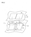
- Fig. 2 is an equivalent circuit diagram of a pixel of the LCD device in Fig. 1.
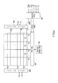
- the LCD device includes a liquid crystal (LC) panel assembly 300, a gate driver 400L and 400R, a data driver 500, a gray voltage generator 800 connected to the data driver 500, a driving voltage generator 900 connected to the gate driver 400L and 400R, and a signal controller 600.
- LC liquid crystal
- the LC panel assembly 300 includes display signal lines G 1 -G n and D 1 -D m and pixels Px connected thereto and arranged in a matrix form.
- the display signal lines G 1 -G n and D 1 -D m include gate lines G 1 -G n transmitting gate signals (or scanning signals) and data lines D 1 -D m transmitting data signals.
- the gate lines G 1 -G n extend in a row direction and are substantially parallel to each other, and the data lines D 1 -D m extend in a column direction and are substantially parallel to each other.
- Each pixel includes one of switching elements Q 1 and Q 2 connected to the display signal lines G 1 -G n and D 1 -D m , an LC capacitor C LC , and a storage capacitor C ST .
- the storage capacitor C ST may be omitted if unnecessary.
- the switching elements Q 1 and Q 2 such as a thin film transistor (TFT), are provided on a lower panel 100 and has three terminals: a control terminal connected to one of the gate lines G 1 -G n ; an input terminal connected to one of the data lines D 1 -D m ; and an output terminal connected to a pixel electrode 190. Furthermore, the switching elements Q 1 and Q2 are in turn connected to left and right side of one of data lines D1-Dm.
- the LC capacitor C LC includes the pixel electrode 190 on the lower panel 100, a common electrode 270 on a upper panel 200, and the LC layer 3 as a dielectric between the electrodes 190 and 270.
- the pixel electrode 190 is connected to the switching elements Q1 and Q2, and the common electrode 270 covers the entire surface of the upper panel 100 and is supplied with a common voltage Vcom.
- both the pixel electrode 190 and the common electrode 270 which have shapes of bars or stripes, are provided on the lower panel 100.
- the storage capacitor C ST is an auxiliary capacitor for the LC capacitor C LC .
- the storage capacitor C ST includes the pixel electrode 190 and a separate signal line (not shown), which is provided on the lower panel 100, overlaps the pixel electrode 190 via an insulator, and is supplied with a predetermined voltage such as the common voltage Vcom.
- the storage capacitor C ST includes the pixel electrode 190 and an adjacent gate line called a previous gate line, which overlaps the pixel electrode 190 via an insulator.
- each pixel uniquely represents one of three primary colors such as red, green and blue colors or sequentially represents the three primary colors in time, thereby obtaining a desired color.
- Fig. 2 shows an example that each pixel includes a color filter 230 representing one of the three primary colors in an area of the upper panel 200 facing its pixel electrode 190. Alternatively, the color filter 230 is provided on or under the pixel electrode 190 on the lower panel 100.
- a polarizer (not shown) polarizing the light is attached on outer side of at least one of the two panels 100 and 200.
- the gray voltage generator 800 generates two sets of gray voltages related to transmittance of the pixels.
- the gray voltages in one set have a positive polarity with respect to the common voltage Vcom, while those in the other set have a negative polarity with respect to the common voltage Vcom.
- the gate drivers 400L and 400R are arranged on left and right side of the LC panel assembly 300 and are respectively connected to the odd gate lines G 1 , G 3 , ..., G 2n-1 and the even gate lines G 2 , G 4 , ..., G 2n . Further, the gate drivers 400L and 400R synthesize the gate-on voltage Von and the gate-off voltage Voff from the driving voltage generator 900 to generate gate signals for application to the gate lines G 1 -G n .
- the data driver 500 is connected to the data lines D 1 -D m of the LC panel assembly 300 and applies data voltages selected from the gray voltages supplied from the gray voltage generator 800 to the data lines D 1 -D m .
- the IC chips of the gate drivers 400L and 400R and/or the data driver 500 are mounted on the lower panel 100. Further, one or more of the drivers 400L and 400R and 500 are incorporated along with other elements into the lower panel 100.
- the gate PCB and/or the gate FPC films may be omitted in both the cases.
- the signal controller 600 is supplied with RGB image signals R, G and B and input control signals controlling the display thereof such as a vertical synchronization signal Vsync, a horizontal synchronization signal Hsync, a main clock MCLK, and a data enable signal DE, from an external graphic controller (not shown).
- the signal controller 600 After generating gate control signals CONT1 and data control signals CONT2 and processing the image signals R, G and B suitable for operation of the LC panel assembly 300 on the basis of the input control signals, the signal controller 600 provides the gate control signals CONT1 for the gate drivers 400L and 400R, the processed image signals R', G' and B' and the data control signals CONT2 for the data driver 500.
- the gate control signals CONTI include a vertical synchronization start signal STV for informing start of a frame, a gate clock signal CPV for controlling an output time of the gate-on voltage Von, and an output enable signal OE for defining width of the gate-on voltage Von.
- the data control signals CONT2 include a horizontal synchronization start signal STH for informing start of a horizontal period, a load signal LOAD or TP for instructing to apply data voltages to the data lines D 1 -D m , an inversion control signal RVS for reversing polarity of the data voltages (with respect to the common voltage Vcom) and a data clock signal HCLK.
- the data driver 500 receives the image data R', G' and B' from the signal controller 600 and converts the image data R', G' and B' into analogue data voltages selected from the gray voltages supplied from the gray voltage generator 800 in response to the data control signals CONT2 from the signal controller 600.
- the gate driver 400 applies the gate-on voltage Von to the gate line G 1 -G n , thereby turning on the switching elements Q1 and Q2 connected thereto.
- the data driver 500 applies the data voltages to the corresponding data lines D 1 -D m for a turn-on time of the switching elements Q (which is called “one horizontal period” or “1H” and equals to one period of the horizontal synchronization signal Hsync, the data enable signal DE, and the gate clock signal CPV). Then, the data voltages are sequentially supplied to the corresponding pixels via the turned-on switching elements Q1 and Q2.
- Difference between the data voltage and the common voltage Vcom applied to a pixel is expressed as a charged voltage of the LC capacitor C LC , i.e., a pixel voltage.
- the liquid crystal molecules have orientations depending on magnitude of the pixel voltage and the orientations determine the polarization of light passing through the LC capacitor C LC .
- the polarizers convert the light polarization into the light transmittance.
- the inversion control signal RVS applied to the data driver 500 is controlled such that polarity of the data voltages is reversed (which is called “frame inversion”).
- the inversion control signal RVS may be also controlled such that polarity of the data voltages flowing in a data line in one frame are reversed (which is called “line inversion”), or polarity of the data voltages in one packet are reversed (which is called “dot inversion").
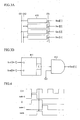
- Fig. 3A is a block diagram of a gate driver according to an embodiment of the present invention
- Fig. 3B is an equivalent circuit diagram of the shift register shown in Fig. 3A
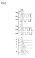
- Fig. 4 is a signal waveforms diagram for illustrating operation of the gate driver shown in Fig. 3.
- the gate drivers 400L and 400R include a plurality of shift registers.
- the shift register 410 may be integrated on the same substrate together when the switching elements of the pixels are formed thereon.
- gate driving ICs are not used, but they are integrated on the LC panel assembly 300.
- the shift register 410 may be represented as a SR latch 411 and an AND gate 412.
- the gate drivers 400L and 400R begin to output the gate-on voltage Von in response to the vertical synchronization start signal STV from the signal controller 600.
- the first shift register 410 begins to output the gate-on voltage Von in synchronization with the vertical synchronization start signal STV and a clock signal CK1, and remainder of the shift registers 410 begin to output the gate-on voltage Von in synchronization with an output voltage of the previous shift register and one of the clock signals CK1 and CK2.
- the SR latch 411 includes a set terminal S which receives a gate output Gout(N-1) of output of the previous shift register and a reset terminal R which receives a gate output Gout(N+1) of output of the following shift register.
- the AND gate 412 generates a gate signal using the output of the SR latch 411 and the clock signal CK1.
- the output of the SR latch 411 is in a low (0) state, too. While the gate output Gout(N+ 1) remains in a low state, the gate output Gout(N-1) changes to a high (1) state, then the output Q of the SR latch 411 changes to a high state, too. While the gate output Gout(N+1) continuously remains in a low state, although the gate output Gout(N-1) changes to a low state again, the output Q of the SR latch 411 does not change.
- the gate output Gout(N-1) While the gate output Gout(N-1) remains in a low state, the gate output Gout(N+1) changes to a high state, then the output Q of the SR latch 411 changes to a low state.
- the output Q of the SR latch 411 remain in a high state from a point of time that the previous gate output Gout(N-1) changes to a high state from a low state to a point of time that the later gate output Gout(N+1) changes to a high state from a low state. However, the output Q of the SR latch 411 remains in a low state except the duration.
- the AND gate 412 generates a gate output Gout(N) of a high state if both the output Q of the SR latch 411 and the clock signal CK1 are in a high state. More in detail, when the gate output Gout(N) remains in a high state and the clock signal changes to a high state from a low state, the gate output Gout(N) changes to a high state. However, when the clock signal CK1 changes to a low state or the output Q of the SR latch 411 changes to a low state, the gate output Gout(N) changes to a low state, too.
- each shift register 410 generates the gate output Gout(N) based on the gate output Gout(N-1) of the previous shift register and the gate output Gout(N+1) of the following shift register, and in synchronization with one of the clock signals CK1 and CK2.
- Adjacent shift registers 410 receive a different one of the clock signals CK1 and CK2, respectively.
- the clock signals CK1 and CK2 each have an opposite phase.
- the gate output Gout(N) is applied to the gate lines for turning on the switching elements Q1 and Q2.
- Fig. 5 is a waveform diagram according to an embodiment of the present invention.
- the signal controller 600 applies the vertical synchronization start signal STVL to the gate driver 400L first, and after the elapsed time of 1/2 H, it applies the vertical synchronization start signal STVR to the gate driver 400R.
- the signal controller 600 applies the clock signals CK1L and CK2L to the gate driver 400L, and after the elapsed time of 1/2 H, it applies the clock signals CK1R and CK2R to the gate driver 400R.
- the gate drivers 400L and 400R operate with an interval of 1/2 H when the vertical synchronization start signals STVL and STVR and the clock signals CK1L, CK1R, CK2L and CK2R are applied with an interval of 1/2 H, respectively. Then, the duration of a high state becomes 1H and the adjacent gate signals are overlapped during 1/2 H.
- the data driver 500 applies the data voltages to the pixels connected to the left and right of the data line Di, and each time for applying the data voltages to pixels connected to the gate drivers 400L and 400R is 1/2 H.
- the gate-on voltage Von is applied to one gate line during 1H and the data voltage is applied during the latter 1/2 H of 1H. Therefore, total time for applying the data voltages to pixels connected to the gate drivers 400L and 400R is 1H.
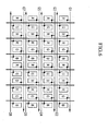
- Fig. 6 is a layout according to an embodiment of the present invention. As shown in Fig. 6, pixels with the same color are connected to the same gate drivers 400L and 400R. For example, red pixels R in the first column are all connected to the gate driver 400L and green pixels G in the second column are all connected to the gate driver 400R. In this way, it is possible to minimize display distortion owing to delay of the gate signal by connecting the pixels with the same color arranged up and down to the same gate drivers 400L and 400R.
- the signal controller 600 stores data in a row to a line memory, and then, divides the data into data of pixels connected to the odd gate lines G1, G3, ... and data of pixels connected the even gate lines G2, G4, ... and supplies them to the data driver 500.
- the data driver 500 applies data voltages with opposite polarities each other to the left and the right pixels connected to one data line. In this manner, it is possible to reduce cost of the data driving ICs by sharing the data line and an output buffer (now shown) with two pixels and perform the dot inversion capable of implementing high quality.
- the shift register 410 is formed together with the switching element Q of the pixel to reduce the number of the gate driving ICs. Also, it is possible to implement lower shift speed than that of a shift register made of poly silicon and to apply the data voltages at the substantially same speed as the shift register made of poly silicon.
Landscapes
- Engineering & Computer Science (AREA)
- Chemical & Material Sciences (AREA)
- Crystallography & Structural Chemistry (AREA)
- Physics & Mathematics (AREA)
- Computer Hardware Design (AREA)
- General Physics & Mathematics (AREA)
- Theoretical Computer Science (AREA)
- Control Of Indicators Other Than Cathode Ray Tubes (AREA)
- Liquid Crystal Display Device Control (AREA)
- Liquid Crystal (AREA)
- Shift Register Type Memory (AREA)
Applications Claiming Priority (2)
| Application Number | Priority Date | Filing Date | Title |
|---|---|---|---|
| KR1020030040684A KR100945581B1 (ko) | 2003-06-23 | 2003-06-23 | 액정 표시 장치 및 그 구동 방법 |
| KR2003040684 | 2003-06-23 |
Publications (2)
| Publication Number | Publication Date |
|---|---|
| EP1492078A2 true EP1492078A2 (de) | 2004-12-29 |
| EP1492078A3 EP1492078A3 (de) | 2006-05-17 |
Family
ID=33411774
Family Applications (1)
| Application Number | Title | Priority Date | Filing Date |
|---|---|---|---|
| EP04014721A Ceased EP1492078A3 (de) | 2003-06-23 | 2004-06-23 | Anzeigesteuervorrichtung mit unterteilter Gatetreibereinheit und Flüssigkristallanzeigegerät und Verfahren mit Verwendung dieser Anzeigesteuervorrichtung |
Country Status (6)
| Country | Link |
|---|---|
| US (3) | US7385576B2 (de) |
| EP (1) | EP1492078A3 (de) |
| JP (1) | JP2005018066A (de) |
| KR (1) | KR100945581B1 (de) |
| CN (1) | CN100443960C (de) |
| TW (1) | TWI277938B (de) |
Cited By (11)
| Publication number | Priority date | Publication date | Assignee | Title |
|---|---|---|---|---|
| EP1986182A1 (de) | 2007-04-27 | 2008-10-29 | Samsung SDI Co., Ltd. | Flüssigkristallanzeige |
| EP2023331A1 (de) * | 2007-08-07 | 2009-02-11 | Samsung Electronics Co., Ltd. | Anzeigevorrichtung und Verfahren zu ihrer Ansteuerung |
| US7561150B2 (en) * | 2004-10-06 | 2009-07-14 | Alps Electric Co., Ltd. | Liquid crystal driving circuit and liquid crystal display device |
| EP1901277A3 (de) * | 2006-09-18 | 2009-10-07 | Samsung Electronics Co., Ltd. | Anzeigevorrichtung |
| EP1901278A3 (de) * | 2006-09-18 | 2009-11-11 | Samsung Electronics Co., Ltd. | Array-Substrat und Anzeigevorrichtung damit |
| EP1970888A3 (de) * | 2007-03-14 | 2011-03-16 | Samsung Electronics Co., Ltd. | Flüssigkristallanzeige |
| US8188963B2 (en) | 2006-06-19 | 2012-05-29 | Lg Display Co., Ltd. | Driving circuit for liquid crystal display device and method of driving the same |
| EP2833352A3 (de) * | 2013-08-02 | 2015-03-04 | Samsung Display Co., Ltd. | Anzeigevorrichtung und Verfahren zu ihrer Ansteuerung |
| EP3054445A3 (de) * | 2015-02-03 | 2016-11-09 | Samsung Display Co., Ltd. | Anzeigebildschirm und anzeigevorrichtung damit |
| EP3193325A1 (de) * | 2015-12-30 | 2017-07-19 | LG Display Co., Ltd. | Flüssigkristallanzeigevorrichtung |
| GB2604221A (en) * | 2020-12-31 | 2022-08-31 | Lg Display Co Ltd | Display apparatus |
Families Citing this family (77)
| Publication number | Priority date | Publication date | Assignee | Title |
|---|---|---|---|---|
| JP4790292B2 (ja) * | 2004-10-25 | 2011-10-12 | 三星電子株式会社 | アレイ基板及びこれを有する表示装置 |
| KR101166580B1 (ko) * | 2004-12-31 | 2012-07-18 | 엘지디스플레이 주식회사 | 액정표시소자 |
| KR101112213B1 (ko) * | 2005-03-30 | 2012-02-27 | 삼성전자주식회사 | 게이트 구동회로 및 이를 갖는 표시장치 |
| US8619007B2 (en) | 2005-03-31 | 2013-12-31 | Lg Display Co., Ltd. | Electro-luminescence display device for implementing compact panel and driving method thereof |
| DE102006014873B4 (de) | 2005-03-31 | 2019-01-03 | Lg Display Co., Ltd. | Ansteuerungsverfahren für eine Elektrolumineszenz-Anzeigevorrichtung |
| US7586476B2 (en) | 2005-06-15 | 2009-09-08 | Lg. Display Co., Ltd. | Apparatus and method for driving liquid crystal display device |
| KR101147091B1 (ko) * | 2005-06-15 | 2012-05-17 | 엘지디스플레이 주식회사 | 액정 표시장치의 구동장치 |
| KR101261603B1 (ko) | 2005-08-03 | 2013-05-06 | 삼성디스플레이 주식회사 | 표시 장치 |
| KR101189273B1 (ko) * | 2005-09-07 | 2012-10-09 | 삼성디스플레이 주식회사 | 표시 장치의 구동 장치 및 이를 포함하는 표시 장치 |
| KR100759476B1 (ko) * | 2005-09-20 | 2007-09-20 | 이디텍 주식회사 | 액정표시 장치 및 그 구동 방법 |
| TWI291153B (en) * | 2005-09-26 | 2007-12-11 | Au Optronics Corp | Display panels, driving method thereof and electronic devices using the same |
| KR101211219B1 (ko) * | 2005-10-31 | 2012-12-11 | 엘지디스플레이 주식회사 | 액정표시장치와 그 구동방법 |
| KR101196860B1 (ko) | 2006-01-13 | 2012-11-01 | 삼성디스플레이 주식회사 | 액정 표시 장치 |
| KR101256921B1 (ko) * | 2006-02-06 | 2013-04-25 | 삼성디스플레이 주식회사 | 게이트 구동유닛 및 이를 갖는 표시장치 |
| KR101222964B1 (ko) * | 2006-02-14 | 2013-01-17 | 엘지디스플레이 주식회사 | 액정표시장치 및 이의 구동방법 |
| KR101206724B1 (ko) | 2006-02-23 | 2012-11-30 | 삼성디스플레이 주식회사 | 표시 장치 |
| KR100775219B1 (ko) * | 2006-03-10 | 2007-11-12 | 엘지이노텍 주식회사 | 인터페이스 장치 및 인터페이스 방법 |
| KR101234422B1 (ko) * | 2006-05-11 | 2013-02-18 | 엘지디스플레이 주식회사 | 액정표시장치 및 그의 구동방법 |
| TWI274212B (en) * | 2006-06-14 | 2007-02-21 | Au Optronics Corp | Liquid crystal display panel and driving method thereof |
| KR101243804B1 (ko) * | 2006-06-30 | 2013-03-18 | 엘지디스플레이 주식회사 | 액정 표시장치의 구동장치 및 구동방법 |
| KR101261607B1 (ko) | 2006-07-25 | 2013-05-08 | 삼성디스플레이 주식회사 | 액정 표시 장치 |
| US7605793B2 (en) * | 2006-08-29 | 2009-10-20 | Tpo Displays Corp. | Systems for display images including two gate drivers disposed on opposite sides of a pixel array |
| TWI341505B (en) * | 2006-11-27 | 2011-05-01 | Chimei Innolux Corp | Liquid crystal panel and driving method thereof |
| KR101345728B1 (ko) * | 2006-12-04 | 2013-12-30 | 삼성디스플레이 주식회사 | 표시장치 |
| TWI360087B (en) * | 2007-02-13 | 2012-03-11 | Au Optronics Corp | Display panel |
| JP5214601B2 (ja) * | 2007-06-12 | 2013-06-19 | シャープ株式会社 | 液晶表示装置、液晶表示装置の駆動方法、及びテレビジョン受像機 |
| JP4890614B2 (ja) * | 2007-06-12 | 2012-03-07 | シャープ株式会社 | 液晶表示装置、液晶表示装置の駆動方法、およびテレビジョン受像機 |
| KR101432717B1 (ko) * | 2007-07-20 | 2014-08-21 | 삼성디스플레이 주식회사 | 표시 장치 및 이의 구동 방법 |
| JP2009063881A (ja) * | 2007-09-07 | 2009-03-26 | Mitsubishi Electric Corp | 液晶表示装置およびその駆動方法 |
| TWI411834B (zh) * | 2007-10-19 | 2013-10-11 | Au Optronics Corp | 液晶顯示裝置及其驅動方法 |
| JP5100450B2 (ja) * | 2007-11-29 | 2012-12-19 | 三菱電機株式会社 | 画像表示装置及びその駆動方法 |
| KR101289634B1 (ko) * | 2007-12-29 | 2013-07-30 | 엘지디스플레이 주식회사 | 액정표시장치와 그 구동방법 |
| JP2009181100A (ja) * | 2008-02-01 | 2009-08-13 | Hitachi Displays Ltd | 液晶表示装置 |
| US8248352B2 (en) * | 2008-04-25 | 2012-08-21 | Lg Display Co., Ltd. | Driving circuit of liquid crystal display |
| KR101366851B1 (ko) * | 2008-04-25 | 2014-02-24 | 엘지디스플레이 주식회사 | 액정표시장치 |
| CN101592831B (zh) * | 2008-05-28 | 2012-11-28 | 群康科技(深圳)有限公司 | 液晶显示器及其驱动方法 |
| TWI397038B (zh) * | 2008-11-05 | 2013-05-21 | Au Optronics Corp | 使用半源極驅動架構之顯示面板及其顯示資料供應方法 |
| KR101341906B1 (ko) * | 2008-12-23 | 2013-12-13 | 엘지디스플레이 주식회사 | 액정 표시장치의 구동장치와 그 구동방법 |
| TWI410939B (zh) * | 2008-12-26 | 2013-10-01 | Au Optronics Corp | 液晶顯示面板驅動方法 |
| TW201042625A (en) * | 2009-05-27 | 2010-12-01 | Au Optronics Corp | Liquid crystal display device and liquid crystal display panel thereof |
| KR102071057B1 (ko) | 2009-06-25 | 2020-01-29 | 가부시키가이샤 한도오따이 에네루기 켄큐쇼 | 표시 장치 |
| TWI412012B (zh) * | 2009-07-20 | 2013-10-11 | Au Optronics Corp | 液晶顯示器 |
| TWI407400B (zh) * | 2009-09-14 | 2013-09-01 | Au Optronics Corp | 液晶顯示器、平面顯示器及其閘極驅動方法 |
| KR101654834B1 (ko) | 2009-11-05 | 2016-09-07 | 삼성디스플레이 주식회사 | 박막 트랜지스터 표시판 및 그 제조 방법 |
| TWI405161B (zh) | 2009-12-17 | 2013-08-11 | Au Optronics Corp | 主動式矩陣顯示器 |
| JPWO2011152138A1 (ja) * | 2010-06-02 | 2013-07-25 | シャープ株式会社 | 表示パネル、表示装置、およびその駆動方法 |
| KR101761861B1 (ko) | 2010-06-18 | 2017-07-27 | 삼성디스플레이 주식회사 | 접촉 감지 기능이 있는 표시 장치 |
| KR101349781B1 (ko) * | 2010-07-01 | 2014-01-09 | 엘지디스플레이 주식회사 | 게이트 구동부 및 이를 포함하는 액정표시장치 |
| JP5620211B2 (ja) * | 2010-09-24 | 2014-11-05 | 株式会社ジャパンディスプレイ | 液晶表示装置 |
| CN101996602A (zh) * | 2010-10-15 | 2011-03-30 | 深圳市华星光电技术有限公司 | 液晶显示器及其驱动显示方法 |
| KR101773934B1 (ko) * | 2010-10-21 | 2017-09-04 | 삼성디스플레이 주식회사 | 표시 패널 및 이를 포함하는 표시 장치 |
| TWI423241B (zh) * | 2010-12-27 | 2014-01-11 | Au Optronics Corp | 液晶顯示裝置之驅動方法 |
| TWI421850B (zh) * | 2010-12-31 | 2014-01-01 | Au Optronics Corp | 液晶顯示裝置以及畫素驅動方法 |
| CN102222484B (zh) * | 2011-05-25 | 2012-11-28 | 深超光电(深圳)有限公司 | 双闸极液晶显示面板驱动方法 |
| KR101909675B1 (ko) | 2011-10-11 | 2018-10-19 | 삼성디스플레이 주식회사 | 표시 장치 |
| JP5963551B2 (ja) * | 2012-06-06 | 2016-08-03 | キヤノン株式会社 | アクティブマトリクスパネル、検出装置、及び、検出システム |
| KR101982167B1 (ko) | 2012-06-21 | 2019-05-27 | 삼성디스플레이 주식회사 | 액정 표시 장치 |
| CN103474039B (zh) * | 2013-08-20 | 2016-09-28 | 北京京东方光电科技有限公司 | 栅线驱动方法、栅极驱动电路以及显示装置 |
| KR102202128B1 (ko) | 2014-01-08 | 2021-01-14 | 삼성디스플레이 주식회사 | 액정표시장치와 그 구동방법 |
| TWI512717B (zh) * | 2014-05-13 | 2015-12-11 | Au Optronics Corp | 多相閘極驅動器及其顯示面板 |
| KR102235609B1 (ko) * | 2014-12-08 | 2021-04-02 | 삼성전자주식회사 | Mram 기반의 프레임 버퍼링 장치, 그 장치를 포함하는 디스플레이 구동 장치 및 디스플레이 장치 |
| JP5905625B1 (ja) * | 2015-05-14 | 2016-04-20 | ミサワホーム株式会社 | シート挟持装置 |
| CN104934006B (zh) * | 2015-07-01 | 2017-09-29 | 京东方科技集团股份有限公司 | 显示面板及其驱动方法、显示装置 |
| US10078405B2 (en) * | 2015-07-28 | 2018-09-18 | Apple Inc. | Displays with gate driver circuitry for discharging display pixels |
| CN105511184B (zh) * | 2016-01-13 | 2019-04-02 | 深圳市华星光电技术有限公司 | 液晶显示面板及其驱动方法 |
| KR102486413B1 (ko) * | 2016-06-15 | 2023-01-10 | 삼성디스플레이 주식회사 | 표시 패널 및 이를 포함하는 표시 장치 |
| CN107665863B (zh) * | 2016-07-29 | 2020-02-07 | 京东方科技集团股份有限公司 | 像素结构及制作方法、阵列基板及制作方法和显示装置 |
| CN106128387A (zh) * | 2016-08-29 | 2016-11-16 | 武汉华星光电技术有限公司 | 液晶显示器及其扫描驱动方法 |
| CN106229319A (zh) * | 2016-09-05 | 2016-12-14 | 京东方科技集团股份有限公司 | 阵列基板及其制造方法、显示面板和显示装置 |
| CN106782411B (zh) * | 2017-02-22 | 2019-02-12 | 京东方科技集团股份有限公司 | 预充电时间调节装置、方法、显示驱动电路和显示装置 |
| KR102458156B1 (ko) * | 2017-08-31 | 2022-10-21 | 엘지디스플레이 주식회사 | 표시 장치 |
| CN108169970B (zh) * | 2018-01-02 | 2022-02-18 | 京东方科技集团股份有限公司 | 显示基板及其驱动方法、显示装置 |
| TWI660335B (zh) * | 2018-05-16 | 2019-05-21 | 友達光電股份有限公司 | 顯示面板 |
| US11847988B2 (en) * | 2019-08-02 | 2023-12-19 | Sitronix Technology Corporation | Driving method for flicker suppression of display panel and driving circuit thereof |
| KR102771824B1 (ko) * | 2020-12-24 | 2025-02-26 | 엘지디스플레이 주식회사 | 게이트 구동 회로 및 표시 장치 |
| CN116169155A (zh) * | 2021-11-25 | 2023-05-26 | 成都辰显光电有限公司 | 显示面板和显示装置 |
| US20250308423A1 (en) * | 2024-04-02 | 2025-10-02 | Samsung Display Co., Ltd. | Display device and electronic device including the same |
Citations (3)
| Publication number | Priority date | Publication date | Assignee | Title |
|---|---|---|---|---|
| JPH08248385A (ja) * | 1995-03-08 | 1996-09-27 | Hitachi Ltd | アクティブマトリックス型液晶ディスプレイとその駆動方法 |
| US20010015715A1 (en) * | 1998-05-07 | 2001-08-23 | Hiroyuki Hebiguchi | Active matrix type liquid crystal display device, and substrate for the same |
| US20030043104A1 (en) * | 2001-09-03 | 2003-03-06 | Samsung Electronics Co., Ltd. | Liquid crystal display apparatus |
Family Cites Families (19)
| Publication number | Priority date | Publication date | Assignee | Title |
|---|---|---|---|---|
| JP2581796B2 (ja) * | 1988-04-25 | 1997-02-12 | 株式会社日立製作所 | 表示装置及び液晶表示装置 |
| JP2623012B2 (ja) * | 1989-10-18 | 1997-06-25 | 三洋電機株式会社 | 液晶表示装置 |
| JPH04324418A (ja) * | 1991-04-25 | 1992-11-13 | Toshiba Corp | アクティブマトリックス型表示装置用駆動回路 |
| JP3091300B2 (ja) * | 1992-03-19 | 2000-09-25 | 富士通株式会社 | アクティブマトリクス型液晶表示装置及びその駆動回路 |
| JPH06148680A (ja) * | 1992-11-09 | 1994-05-27 | Hitachi Ltd | マトリクス型液晶表示装置 |
| JPH07199154A (ja) * | 1993-12-29 | 1995-08-04 | Casio Comput Co Ltd | 液晶表示装置 |
| FR2719936B1 (fr) * | 1994-05-10 | 1996-07-26 | Sagem | Dispositif de visualisation à cristaux liquides, à matrice active. |
| JP2937130B2 (ja) * | 1996-08-30 | 1999-08-23 | 日本電気株式会社 | アクティブマトリクス型液晶表示装置 |
| GB2345207A (en) * | 1998-12-22 | 2000-06-28 | Sharp Kk | Static clock pulse generator for LCD |
| JP3800863B2 (ja) * | 1999-06-02 | 2006-07-26 | カシオ計算機株式会社 | 表示装置 |
| KR100291770B1 (ko) * | 1999-06-04 | 2001-05-15 | 권오경 | 액정표시장치 |
| KR100661826B1 (ko) * | 1999-12-31 | 2006-12-27 | 엘지.필립스 엘시디 주식회사 | 액정표시장치 |
| JP2002023683A (ja) * | 2000-07-07 | 2002-01-23 | Sony Corp | 表示装置およびその駆動方法 |
| JP2002049360A (ja) * | 2000-08-02 | 2002-02-15 | Victor Co Of Japan Ltd | 液晶表示装置 |
| TWI277057B (en) * | 2000-10-23 | 2007-03-21 | Semiconductor Energy Lab | Display device |
| JP2002175056A (ja) * | 2000-12-07 | 2002-06-21 | Hitachi Ltd | 液晶表示装置 |
| JP2002202760A (ja) | 2000-12-27 | 2002-07-19 | Nec Corp | 液晶表示装置の駆動方法及び駆動回路 |
| KR100752602B1 (ko) * | 2001-02-13 | 2007-08-29 | 삼성전자주식회사 | 쉬프트 레지스터와, 이를 이용한 액정 표시 장치 |
| KR100884992B1 (ko) * | 2002-04-20 | 2009-02-20 | 엘지디스플레이 주식회사 | 액정표시장치 |
-
2003
- 2003-06-23 KR KR1020030040684A patent/KR100945581B1/ko not_active Expired - Fee Related
-
2004
- 2004-06-23 TW TW093118104A patent/TWI277938B/zh not_active IP Right Cessation
- 2004-06-23 US US10/875,147 patent/US7385576B2/en active Active
- 2004-06-23 CN CNB2004100684680A patent/CN100443960C/zh not_active Expired - Lifetime
- 2004-06-23 EP EP04014721A patent/EP1492078A3/de not_active Ceased
- 2004-06-23 JP JP2004184686A patent/JP2005018066A/ja active Pending
-
2008
- 2008-05-06 US US12/115,937 patent/US8274460B2/en active Active
-
2012
- 2012-08-27 US US13/595,318 patent/US20130215097A1/en not_active Abandoned
Patent Citations (3)
| Publication number | Priority date | Publication date | Assignee | Title |
|---|---|---|---|---|
| JPH08248385A (ja) * | 1995-03-08 | 1996-09-27 | Hitachi Ltd | アクティブマトリックス型液晶ディスプレイとその駆動方法 |
| US20010015715A1 (en) * | 1998-05-07 | 2001-08-23 | Hiroyuki Hebiguchi | Active matrix type liquid crystal display device, and substrate for the same |
| US20030043104A1 (en) * | 2001-09-03 | 2003-03-06 | Samsung Electronics Co., Ltd. | Liquid crystal display apparatus |
Cited By (22)
| Publication number | Priority date | Publication date | Assignee | Title |
|---|---|---|---|---|
| US7561150B2 (en) * | 2004-10-06 | 2009-07-14 | Alps Electric Co., Ltd. | Liquid crystal driving circuit and liquid crystal display device |
| USRE43850E1 (en) | 2004-10-06 | 2012-12-11 | Onanovich Group Ag, Llc | Liquid crystal driving circuit and liquid crystal display device |
| US8188963B2 (en) | 2006-06-19 | 2012-05-29 | Lg Display Co., Ltd. | Driving circuit for liquid crystal display device and method of driving the same |
| EP1901277A3 (de) * | 2006-09-18 | 2009-10-07 | Samsung Electronics Co., Ltd. | Anzeigevorrichtung |
| EP1901278A3 (de) * | 2006-09-18 | 2009-11-11 | Samsung Electronics Co., Ltd. | Array-Substrat und Anzeigevorrichtung damit |
| US7816683B2 (en) | 2006-09-18 | 2010-10-19 | Samsung Electronics Co., Ltd. | Array substrate and display apparatus having the same |
| US8194057B2 (en) | 2006-09-18 | 2012-06-05 | Samsung Electronics Co., Ltd. | Display apparatus |
| US8823622B2 (en) | 2007-03-14 | 2014-09-02 | Samsung Display Co., Ltd. | Liquid crystal display |
| EP1970888A3 (de) * | 2007-03-14 | 2011-03-16 | Samsung Electronics Co., Ltd. | Flüssigkristallanzeige |
| US8994627B2 (en) | 2007-04-27 | 2015-03-31 | Samsung Display Co., Ltd. | Liquid crystal display |
| EP1986182A1 (de) | 2007-04-27 | 2008-10-29 | Samsung SDI Co., Ltd. | Flüssigkristallanzeige |
| US8698722B2 (en) | 2007-08-07 | 2014-04-15 | Samsung Display Co., Ltd. | Display apparatus and driving method thereof |
| EP2023331A1 (de) * | 2007-08-07 | 2009-02-11 | Samsung Electronics Co., Ltd. | Anzeigevorrichtung und Verfahren zu ihrer Ansteuerung |
| EP2833352A3 (de) * | 2013-08-02 | 2015-03-04 | Samsung Display Co., Ltd. | Anzeigevorrichtung und Verfahren zu ihrer Ansteuerung |
| US9812088B2 (en) | 2013-08-02 | 2017-11-07 | Samsung Display Co., Ltd. | Display device including gray scale corrector and driving method thereof |
| EP3054445A3 (de) * | 2015-02-03 | 2016-11-09 | Samsung Display Co., Ltd. | Anzeigebildschirm und anzeigevorrichtung damit |
| US10242633B2 (en) | 2015-02-03 | 2019-03-26 | Samsung Display Co., Ltd. | Display panel and a display apparatus including the same |
| EP3193325A1 (de) * | 2015-12-30 | 2017-07-19 | LG Display Co., Ltd. | Flüssigkristallanzeigevorrichtung |
| US10176775B2 (en) | 2015-12-30 | 2019-01-08 | Lg Display Co., Ltd. | Display device |
| GB2604221A (en) * | 2020-12-31 | 2022-08-31 | Lg Display Co Ltd | Display apparatus |
| US11721300B2 (en) | 2020-12-31 | 2023-08-08 | Lg Display Co., Ltd. | Display apparatus in which gate pulses are outputted sequentially to alternate sides of a gate line |
| GB2604221B (en) * | 2020-12-31 | 2023-11-29 | Lg Display Co Ltd | Display apparatus |
Also Published As
| Publication number | Publication date |
|---|---|
| US20040257322A1 (en) | 2004-12-23 |
| KR100945581B1 (ko) | 2010-03-08 |
| US20130215097A1 (en) | 2013-08-22 |
| US7385576B2 (en) | 2008-06-10 |
| TWI277938B (en) | 2007-04-01 |
| TW200509052A (en) | 2005-03-01 |
| JP2005018066A (ja) | 2005-01-20 |
| CN100443960C (zh) | 2008-12-17 |
| EP1492078A3 (de) | 2006-05-17 |
| US8274460B2 (en) | 2012-09-25 |
| KR20050000105A (ko) | 2005-01-03 |
| CN1573459A (zh) | 2005-02-02 |
| US20080204390A1 (en) | 2008-08-28 |
Similar Documents
| Publication | Publication Date | Title |
|---|---|---|
| US7385576B2 (en) | Display driving device and method and liquid crystal display apparatus having the same | |
| US8212802B2 (en) | Driving apparatus of display device and display device including the same | |
| US8354989B2 (en) | Liquid crystal display panel and display apparatus having the same | |
| JP5483517B2 (ja) | 液晶表示装置 | |
| CN100367085C (zh) | 液晶显示器件及其驱动方法 | |
| US20070052658A1 (en) | Driver for display apparatus and display apparatus including the same | |
| KR20080006037A (ko) | 시프트 레지스터, 이를 포함하는 표시 장치, 시프트레지스터의 구동 방법 및 표시 장치의 구동 방법 | |
| US20100123702A1 (en) | Liquid crystal display and method of driving the same | |
| US20060279506A1 (en) | Apparatus and method of driving liquid crystal display apparatus | |
| US20050078075A1 (en) | Display apparatus, method and device of driving the same | |
| JP2006154715A (ja) | 液晶表示装置及びその駆動方法 | |
| KR20070039759A (ko) | 액정 표시 장치 | |
| US8040314B2 (en) | Driving apparatus for liquid crystal display | |
| KR20050077573A (ko) | 액정 표시 장치 | |
| KR101290017B1 (ko) | 액정표시장치와 그 구동방법 | |
| KR20070063168A (ko) | 액정 표시 장치 및 그 구동 방법 | |
| KR20070081164A (ko) | 액정 표시 장치 | |
| KR20070070639A (ko) | 표시 장치의 구동 장치 | |
| KR20040014002A (ko) | 액정 표시 장치 및 그 구동 방법 | |
| KR20070111150A (ko) | 액정 표시 장치 | |
| KR20070027374A (ko) | 표시 장치의 구동 장치 | |
| KR20070063944A (ko) | 표시 장치 | |
| KR20070066450A (ko) | 액정 표시 장치 | |
| KR20070093240A (ko) | 액정 표시 장치 | |
| KR20070087301A (ko) | 액정 표시 장치 |
Legal Events
| Date | Code | Title | Description |
|---|---|---|---|
| PUAI | Public reference made under article 153(3) epc to a published international application that has entered the european phase |
Free format text: ORIGINAL CODE: 0009012 |
|
| AK | Designated contracting states |
Kind code of ref document: A2 Designated state(s): AT BE BG CH CY CZ DE DK EE ES FI FR GB GR HU IE IT LI LU MC NL PL PT RO SE SI SK TR |
|
| AX | Request for extension of the european patent |
Extension state: AL HR LT LV MK |
|
| PUAL | Search report despatched |
Free format text: ORIGINAL CODE: 0009013 |
|
| AK | Designated contracting states |
Kind code of ref document: A3 Designated state(s): AT BE BG CH CY CZ DE DK EE ES FI FR GB GR HU IE IT LI LU MC NL PL PT RO SE SI SK TR |
|
| AX | Request for extension of the european patent |
Extension state: AL HR LT LV MK |
|
| 17P | Request for examination filed |
Effective date: 20061027 |
|
| AKX | Designation fees paid |
Designated state(s): DE FR GB |
|
| 17Q | First examination report despatched |
Effective date: 20080627 |
|
| RAP1 | Party data changed (applicant data changed or rights of an application transferred) |
Owner name: SAMSUNG ELECTRONICS CO., LTD. |
|
| RAP1 | Party data changed (applicant data changed or rights of an application transferred) |
Owner name: SAMSUNG DISPLAY CO., LTD. |
|
| RAP1 | Party data changed (applicant data changed or rights of an application transferred) |
Owner name: SAMSUNG DISPLAY CO., LTD. |
|
| STAA | Information on the status of an ep patent application or granted ep patent |
Free format text: STATUS: THE APPLICATION HAS BEEN REFUSED |
|
| 18R | Application refused |
Effective date: 20180925 |