EP1492119A2 - DVD Gerät - Google Patents
DVD Gerät Download PDFInfo
- Publication number
- EP1492119A2 EP1492119A2 EP04014744A EP04014744A EP1492119A2 EP 1492119 A2 EP1492119 A2 EP 1492119A2 EP 04014744 A EP04014744 A EP 04014744A EP 04014744 A EP04014744 A EP 04014744A EP 1492119 A2 EP1492119 A2 EP 1492119A2
- Authority
- EP
- European Patent Office
- Prior art keywords
- circuit board
- printed circuit
- optical disk
- digital circuit
- power supply
- Prior art date
- Legal status (The legal status is an assumption and is not a legal conclusion. Google has not performed a legal analysis and makes no representation as to the accuracy of the status listed.)
- Ceased
Links
Images





Classifications
-
- G—PHYSICS
- G11—INFORMATION STORAGE
- G11B—INFORMATION STORAGE BASED ON RELATIVE MOVEMENT BETWEEN RECORD CARRIER AND TRANSDUCER
- G11B33/00—Constructional parts, details or accessories not provided for in the other groups of this subclass
- G11B33/12—Disposition of constructional parts in the apparatus, e.g. of power supply, of modules
- G11B33/121—Disposition of constructional parts in the apparatus, e.g. of power supply, of modules the apparatus comprising a single recording/reproducing device
-
- G—PHYSICS
- G11—INFORMATION STORAGE
- G11B—INFORMATION STORAGE BASED ON RELATIVE MOVEMENT BETWEEN RECORD CARRIER AND TRANSDUCER
- G11B33/00—Constructional parts, details or accessories not provided for in the other groups of this subclass
- G11B33/14—Reducing influence of physical parameters, e.g. temperature change, moisture, dust
- G11B33/1493—Electro-Magnetic Interference [EMI] or Radio Frequency Interference [RFI] shielding; grounding of static charges
-
- H—ELECTRICITY
- H05—ELECTRIC TECHNIQUES NOT OTHERWISE PROVIDED FOR
- H05K—PRINTED CIRCUITS; CASINGS OR CONSTRUCTIONAL DETAILS OF ELECTRIC APPARATUS; MANUFACTURE OF ASSEMBLAGES OF ELECTRICAL COMPONENTS
- H05K1/00—Printed circuits
- H05K1/02—Details
- H05K1/0213—Electrical arrangements not otherwise provided for
- H05K1/0216—Reduction of cross-talk, noise or electromagnetic interference
-
- H—ELECTRICITY
- H05—ELECTRIC TECHNIQUES NOT OTHERWISE PROVIDED FOR
- H05K—PRINTED CIRCUITS; CASINGS OR CONSTRUCTIONAL DETAILS OF ELECTRIC APPARATUS; MANUFACTURE OF ASSEMBLAGES OF ELECTRICAL COMPONENTS
- H05K1/00—Printed circuits
- H05K1/02—Details
- H05K1/14—Structural association of two or more printed circuits
-
- H—ELECTRICITY
- H05—ELECTRIC TECHNIQUES NOT OTHERWISE PROVIDED FOR
- H05K—PRINTED CIRCUITS; CASINGS OR CONSTRUCTIONAL DETAILS OF ELECTRIC APPARATUS; MANUFACTURE OF ASSEMBLAGES OF ELECTRICAL COMPONENTS
- H05K2201/00—Indexing scheme relating to printed circuits covered by H05K1/00
- H05K2201/09—Shape and layout
- H05K2201/09209—Shape and layout details of conductors
- H05K2201/0929—Conductive planes
- H05K2201/093—Layout of power planes, ground planes or power supply conductors, e.g. having special clearance holes therein
-
- H—ELECTRICITY
- H05—ELECTRIC TECHNIQUES NOT OTHERWISE PROVIDED FOR
- H05K—PRINTED CIRCUITS; CASINGS OR CONSTRUCTIONAL DETAILS OF ELECTRIC APPARATUS; MANUFACTURE OF ASSEMBLAGES OF ELECTRICAL COMPONENTS
- H05K2201/00—Indexing scheme relating to printed circuits covered by H05K1/00
- H05K2201/09—Shape and layout
- H05K2201/09209—Shape and layout details of conductors
- H05K2201/09654—Shape and layout details of conductors covering at least two types of conductors provided for in H05K2201/09218 - H05K2201/095
- H05K2201/09663—Divided layout, i.e. conductors divided in two or more parts
Definitions
- the present invention relates to a DVD (Digital Versatile Disc) apparatus.
- the aforementioned conventional approach has a metal shield plate inserted for electromagnetic shielding to prevent electromagnetic interference (EMI).
- EMI electromagnetic interference
- Conventional apparatuses with an appearance of a synthetic resin cabinet took countermeasures against electromagnetic radiation by incorporating the aforementioned shield plate or inserting a metal case inside the resin-made cabinet.
- VCCI Voluntary Control Council for Interference by Data Processing Equipment and Electronic Office Machine
- the limit value for EMI restriction is defined on a country-by-country basis abroad. Therefore, the electric field intensity of unwanted emission in a product must be suppressed below the limit value set at the country where that product is used.
- the problem of unwanted emission is more acute in digital signal processing than in analog signal processing since more harmonics are generated during the processing of digital signals.
- the fundamental frequency of a digital signal corresponds to the operating frequency of the microcomputer for control.
- the operating frequency of such a microcomputer is approximately 12 MHz
- a DVD apparatus has images and sound recorded in digital signals, requiring processing of multibit digital signals, as well as encode and decode processing of MPEG (Motion Picture Experts Group) and the like by means of a memory. Therefore, digital signals are processed at a higher rate than in VCRs.
- the operating frequency of the signal processing system is as high as 54 MHz
- the operating frequency of the memory is as high as 120 MHz
- the limit of unwanted emission is defined to 43.5dB in frequency bands below 220MHz, to 46.0dB in frequency bands of 220-540 MHz, and to 54dB in frequency bands above 540 MHz
- the limit will be alleviated as the frequency becomes higher, the effect of background noise and increase in antenna loss will become more significant. More careful means must be taken to suppress occurrence of unwanted emission as the frequency becomes higher. Otherwise, the limit will be exceeded.
- a DVD apparatus since a DVD apparatus has a higher circuit operating frequency than a VCR, circuitry will respond too sensitively to impulse noise of an extremely small range that was of no concern in conventional VCRs.
- impulse noises originate from electric energy present in nature such as static electricity.
- static electricity and the like will be introduced as radio waves to be received at regions other than the site where the static electricity is directly applied to cause high frequency noise.
- the disadvantage of erroneous operation and the like may occur.
- a metal case functions effectively to reduce the above-described unwanted emission and to provide protection from incident high frequency noise. Therefore, a metal case has been typically employed in conventional cases.
- a conventional DVD player has a rigid U-shape metal panel cover arranged on a metal base.
- the rear side is also made of metal.
- the front panel is formed of plastic so as to accommodate various designs.
- a conventional DVD player is generally cover with a metal panel on all sides except for the front.
- a resin case could not be used for a DVD apparatus as a substitute for a metal case that is disadvantageous from the standpoint of cost as compared to a resin case.
- An object of the present invention is to provide a DVD apparatus competitive in cost by employing a resin case.
- a DVD apparatus includes a first printed circuit board mounted with a power supply circuit that provides a direct power supply voltage used internally, an optical disk loader including a pick up unit to read out information of an optical disk, a second printed circuit board mounted with a digital circuit receiving supply of the direct current power supply voltage from the first printed circuit board to carry out a reproduction process of a video signal and an audio signal on a signal read out from the pick up unit, and providing control of a system, and a resin case storing the first printed circuit board, the optical disk loader, and the second printed circuit board.
- a system LSI integrated with a digital circuit that carries out the reproduction process and that carries out the control of a system is mounted on the surface side of the second printed circuit board.
- the second printed circuit board includes a grounding pattern arranged so as to overlap with at least the mounted region of the system LSI.
- the grounding pattern is formed at an intermediate conductor layer between the surface side and back side of the second printed circuit board.
- the optical disk loader further includes a motor to rotate the optical disk.
- the second printed circuit board further includes a memory connected to the system LSI and a motor driver driving the motor.
- the grounding pattern applies a common ground potential to the system LSI, the memory, and the motor driver.
- the second printed circuit board is of a shape having two pairs of opposite sides, and mounted with a system LSI integrated with a digital circuit that carries out a reproduction process and that provides control of the system.
- the mounting position of the system LSI on the second printed circuit board is located closer to a first side than a second side, both first and second sides constituting one of the two pairs.
- the second printed circuit board is further mounted with a connector provided along the second side to establish electrical connection with the first printed circuit board.
- the DVD apparatus further includes a connector provided on the second printed circuit board, and a signal line connected to the connector.
- the second printed circuit board includes a region to arrange a filter, adjacent to a terminal of the connector connected to the signal line to inhibit radiation of unwanted emission caused by a high frequency signal issued from the digital circuit.
- the optical disk loader is arranged at the center region, and the first and second printed circuit boards are arranged at respective sides of the optical disk loader.
- a main advantage of the present invention is to significantly reduce the level of unwanted emission by dividing the circuit board into a digital circuit board and a power supply circuit board. Accordingly, a metal case is dispensable, allowing the usage of a resin case. Therefore, the cost of a DVD apparatus can be reduced.
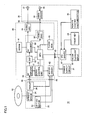
- Fig. 1 is a whole block diagram of a DVD apparatus of the present invention.
- a DVD apparatus 10 includes an optical disk loader 20 to set an optical disk 12, a digital circuit board 40 to process a signal read out from optical disk 12 sent from optical disk loader 20, and a power supply circuit board 30 supplying power to digital circuit board 40.
- Optical disk loader 20 includes a spindle motor 24 to rotate optical disk 12, a pickup 26 to direct a beam onto an optical disk to read out information, and an LD ⁇ feed motor 22 to load a tray for mounting an optical disk not shown and move pickup 26 corresponding to a readout position.
- Digital circuit board 40 includes a system LSI 50 having a front end processing circuit temporarily demodulating a modulated signal from the pickup to form a bit stream, an MPEG (Motion Picture Experts Group) demodulator circuit and a system control microprocessor integrated in one package, an SDRAM (Synchronous Dynamic Random Access Memory) 41 connected to system LSI 50, a flash ROM (Read Only Memory) 43, a motor driver 42, and an audio DAC (Digital-to-Analog Converter) 44.
- system LSI 50 having a front end processing circuit temporarily demodulating a modulated signal from the pickup to form a bit stream
- MPEG Motion Picture Experts Group
- SDRAM Synchronous Dynamic Random Access Memory
- flash ROM Read Only Memory
- motor driver 42 and an audio DAC (Digital-to-Analog Converter) 44.
- System LSI 50 includes an RF amplifier 51 receiving a signal read out from pickup 26, a DSP (Digital Signal Processor) 52 converting the outputs of RF amplifier 51 into a bit stream, an AV decoder 53 decoding the output from DSP 52 into a digital audio signal and video signal, a servo control unit 54 driving motor driver 42 according to an output of RF amplifier 51, and an MPU (Micro Processing Unit) 55 connected to servo control unit 54, DSP 52 and AV decoder 53 to provide entire control of the system.
- DSP Digital Signal Processor
- AV decoder 53 decoding the output from DSP 52 into a digital audio signal and video signal
- MPU Micro Processing Unit
- System LSI 50 further includes a video DAC 56 to convert a digital video signal output from AV decoder 53 into an analog signal.
- SDRAM 41 is connected to AV decoder 53 to be used as a working memory for the MPEG demodulation process.
- Flash ROM 43 is connected to MPU 55, and has a program for system control stored therein.
- Motor driver 42 outputs a driving signal to LD ⁇ feed motor 22, spindle motor 24 and pickup 26 under control of servo control unit 54.
- Audio DAC 44 converts a digital audio signal output from AV decoder 53 into an analog audio signal.
- Power supply circuit board 30 includes a power supply circuit 31 generating and supplying to digital circuit board 40 a stabilized direct current power supply voltage based on an externally applied alternating current power supply, a vacuum fluorescent display (VFD) 33 displaying a reproduction status of the optical disk, a front key 34 to designate playback and stop of an optical disk, a remote control photoreceptor 35 receiving infrared radiation from a remote controller in controlling the operation of an optical disk by remote control operation, and a VFD driver 32 connected to vacuum fluorescent display 33, front key 34 and remote control photoreceptor 35 to drive the VFD under control of MPU 55.
- VFD vacuum fluorescent display
- Power supply circuit board 30 further includes an audio output terminal 37 to provide the output from audio DAC 44 outside, a video driver 36 receiving an output of video DAC 56, and a video output terminal 38 to output a video signal from video driver 36.
- Digital circuit board 40 further includes connectors 45-48.
- Connector 45 is connected with a signal line to transmit a signal from pickup 26 to RF amplifier 51.
- Connector 46 is connected with a signal line connecting LD ⁇ feed motor 22, spindle motor 24 and pickup 26 with motor driver 42.
- Connector 47 is connected with a power supply line supplying power from power supply circuit 31 to digital circuit board 40 and a control signal line connecting MPU 55 and VFD driver 32.
- Connector 48 is connected with a signal line transmitting the output of audio DAC 44 to output terminal 37 and transmitting the output of video DAC 56 to video driver 36.
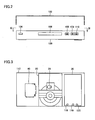
- Fig. 2 is a front view of the DVD apparatus of the present invention.
- a front panel 100 has a power switch 104, a playback button 109, a stop button 110, and an eject button 108 arranged.
- eject button 108 Upon operation of eject button 108, a tray on which an optical disk is to be mounted is ejected frontwards from a loading opening 106.
- the DVD apparatus is covered with a resin case 102.
- the DVD apparatus of the present invention can lower the level of unwanted emission, and can use a resin case 102 for the casing. Accordingly, the cost of the DVD apparatus can be reduced significantly.
- resin case 102 is fit at the chassis case base plate.
- Fig. 2 corresponds to the state where resin case 102 is detached above the chassis.
- Fig. 3 shows an arrangement of the circuit board and the optical disk loader in the DVD apparatus of the present invention.
- Fig. 3 corresponds to a plan view of the DVD apparatus viewed from the plane of III-III of Fig. 2.
- digital circuit board 40 On a chassis case base plate 112 are arranged digital circuit board 40, optical disk loader 20, and power supply circuit board 30.
- Optical disk loader 20 is arranged at the central region with digital circuit board 40 and power supply circuit board 30 at respective sides.
- switches 118, 119 and 120 At the front panel side of power supply circuit board 30 are arranged switches 118, 119 and 120 corresponding to buttons 108, 109 and 110, respectively, of Fig. 2.
- pickup 26 is arranged in a movable manner from the center towards the outer circumference of an optical disk.
- digital circuit board 40 Although an arrangement of digital circuit board 40, optical disk loader 20, and power supply circuit board 30 currently considered to be the best is shown, the characterizing feature is that the digital circuit board is separated from the power supply circuit board. Alternatively, digital circuit board 40 may be placed on power supply circuit board 40, and arranged beside optical disk loader 20.
- Fig. 4 shows the arrangement of main IC components at the surface side of a digital circuit board in the evaluation example.
- system LSI 50 and flash ROM 43 of Fig. 1 are arranged at the surface side of a digital circuit board 540 of the evaluation example. Further, a positioning hole 544 and screw holes 542 and 546 for fixation are provided at digital circuit board 540.
- Fig. 5 is a perspective illustration of the arrangement of main components at the back side of the digital circuit board of the evaluation example, viewed from the surface side.
- SDRAM 41 of Fig. 1 is arranged at digital circuit board 540 with connectors 45-48 of Fig. 1 at the peripheral region.
- connectors 45-48 of Fig. 1 at the peripheral region.
- Fig. 6 shows the grounding pattern of the digital circuit board in the evaluation example.
- the grounding pattern is formed at a conductor layer provided intermediate the surface side and back side of digital circuit board 540.
- the grounding pattern is divided into five patterns 601-605. Although through holes for the connection of upper and lower conductor layers are provided in the grounding pattern, the through holes are not depicted for the sake of convenience.
- Fig. 7 shows the power supply pattern of the digital circuit board in the evaluation example.
- the power supply pattern is formed at an intermediate layer provided intermediate the surface side and back side of digital circuit board 540, differing from that of the grounding pattern.
- the power supply pattern is divided into twelve patterns 651-662. Although through holes are provided for the connection of upper and lower conductor layers in the power supply pattern, the through holes are not depicted for the sake of convenience.
- Fig. 8 shows the level of unwanted emission in an DVD apparatus corresponding to the case where the digital circuit board of the evaluation example is employed.
- Fig. 9 shows an arrangement of main IC components at the surface side of the digital circuit board of the present invention.
- mainly system LSI 50 and flash ROM 43 of Fig. 1 are arranged at the surface of digital circuit board 40.
- a positioning hole 124 and screw holes 122 and 126 for fixation are provided at digital circuit board 40.
- Digital circuit board 40 is partially enlarged in size to evaluate the arrangement of filters that will be described afterwards, as compared to digital circuit board 540 of Fig. 4.
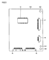
- Fig. 10 is a perspective illustration of the arrangement of main components at the back side of the digital circuit board of the present invention, viewed from the surface side.
- a SDRAM (Synchronous Dynamic Random Access Memory) 41 and connectors 45-48 are arranged on digital circuit board 40, similar to the example of Fig. 5.
- Digital circuit board 40 has a shape including two pairs of opposite sides.
- the mounting position of system LSI 50 on digital circuit board 40 is located closer to a first side than a second side in Fig. 9. These opposite first and second sides constitute one of the pairs.
- digital circuit board 40 has connector 47 mounted along the second side, distant from the mounting position of system LSI 50. Connector 47 establishes electrical connection with the power supply circuit board. A similar relationship applies to the mounting position of the other one connector 48 directed to establishing electrical connection with the power supply circuit board and system LSI 50.
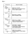
- Fig. 11 is a diagram to describe the types of filters arranged at the filter arrange regions of Fig. 10.
- Type 1 corresponds to an LC filter, employed at a region where the frequency characteristic is of no concern.
- Type 2 corresponds to a capacitor connected between a connection line and the grounding pattern, employed at a region where the impedance of the connection line is high.
- Type 3 corresponds to an RC filter, employed at a region where attention must be paid to the frequency characteristic.
- Type 4 corresponds to an inductance inserted in series with the connection line, employed at a region where direct current characteristic and low frequency characteristic are of much account.
- filters of types 2, 4 and 5 shown in Fig. 11 are arranged at filter arrange region 135 adjacent to thereto.
- filters of types 1 and 4 of Fig. 11 are arranged at filter arrange region 136 adjacent to thereto.
- filters of types 1 and 4 of Fig. 11 are connected at filter arrange region 137 adjacent to thereto.
- filters of types 2, 3, 4 and 5 of Fig. 11 are connected at filter arrange region 138 adjacent to thereto.
- Fig. 12 shows the grounding pattern of the digital circuit board of the present invention.
- the grounding pattern is formed at an intermediate layer provided intermediate the surface side and back side of the digital circuit board.
- Digital circuit board 40 includes two grounding patterns 141 and 142. Although through holes to establish connection between the upper and lower conductor layers are provided at the grounding pattern, the through holes are not depicted for the sake of convenience.
- the four patterns of patterns 601, 603, 604, and 605 are integrated.
- the position of arrangement of system LSI 50, SDRAM 41 and flash ROM 43 is indicated by broken lines. It is appreciated that the region where system LSI 50 is arranged is completely covered with one grounding pattern 141. In other words, the system LSI is arranged on one grounding pattern that is not divided.
- Grounding pattern 141 is depicted as an example where it is formed integrally at an intermediate layer. Alternatively, separate grounding patterns provided at two conductor layers may be connected by a through hole, and cover a region similar to grounding pattern 141.
- grounding pattern 141 By virtue of grounding pattern 141, the unwanted emission from system LSI 50 arranged at the surface side of digital circuit board 40 towards the back side of digital circuit board 40 can be blocked to reduce the level of unwanted emission as a whole.
- Fig. 13 shows a power supply pattern of the digital circuit board in the present invention.
- the power supply pattern is formed at an intermediate layer between the surface side and back side of digital circuit board 40, differing from the layer where the grounding pattern is formed.
- through holes to establish connection between the upper and lower conductor layers are provided at the power supply pattern, the through holes are not depicted for the sake of convenience.
- the power supply pattern is divided into twelve power supply patterns 151-162. It is appreciated that this is similar to that of the evaluation example of Fig. 7. In other words, the power supply pattern is similar to that of the evaluation example, and the divided number of grounding patterns and the filter arrangement are modified in the digital circuit board of the present invention.
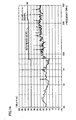
- Fig. 14 represents the level of unwanted emission in a DVD apparatus when the digital circuit board of the present invention is employed.
- the level of unwanted emission is reduced significantly by modifying the division of the grounding pattern of the digital circuit board and arranging filters adjacent to the connector. Accordingly, a metal case is dispensable, and a resin case can be employed. Therefore, the cost of the DVD apparatus can be reduced.
Landscapes
- Engineering & Computer Science (AREA)
- Microelectronics & Electronic Packaging (AREA)
- Physics & Mathematics (AREA)
- Electromagnetism (AREA)
- Structure Of Printed Boards (AREA)
- Optical Head (AREA)
- Optical Recording Or Reproduction (AREA)
Applications Claiming Priority (2)
| Application Number | Priority Date | Filing Date | Title |
|---|---|---|---|
| JP2003179727A JP2005018849A (ja) | 2003-06-24 | 2003-06-24 | Dvd装置 |
| JP2003179727 | 2003-06-24 |
Publications (2)
| Publication Number | Publication Date |
|---|---|
| EP1492119A2 true EP1492119A2 (de) | 2004-12-29 |
| EP1492119A3 EP1492119A3 (de) | 2007-07-04 |
Family
ID=33411060
Family Applications (1)
| Application Number | Title | Priority Date | Filing Date |
|---|---|---|---|
| EP04014744A Ceased EP1492119A3 (de) | 2003-06-24 | 2004-06-23 | DVD Gerät |
Country Status (3)
| Country | Link |
|---|---|
| US (1) | US20040264945A1 (de) |
| EP (1) | EP1492119A3 (de) |
| JP (1) | JP2005018849A (de) |
Families Citing this family (1)
| Publication number | Priority date | Publication date | Assignee | Title |
|---|---|---|---|---|
| JP2013016221A (ja) | 2011-07-01 | 2013-01-24 | Funai Electric Co Ltd | 転送制御装置及び再生装置 |
Family Cites Families (6)
| Publication number | Priority date | Publication date | Assignee | Title |
|---|---|---|---|---|
| US6215076B1 (en) * | 1996-03-28 | 2001-04-10 | Canon Kabushiki Kaisha | Printed circuit board with noise suppression |
| JPH1075416A (ja) * | 1996-08-29 | 1998-03-17 | Alpine Electron Inc | 蓄積型記憶媒体の再生方式 |
| JPH10334643A (ja) * | 1997-05-30 | 1998-12-18 | Toshiba Corp | ディスク再生装置 |
| US6743104B1 (en) * | 1999-11-18 | 2004-06-01 | Nintendo Co., Ltd. | Portable game machine |
| JP2001320181A (ja) * | 2000-05-09 | 2001-11-16 | Sony Computer Entertainment Inc | 電子機器 |
| JP2004527129A (ja) * | 2001-05-03 | 2004-09-02 | トムソン ライセンシング ソシエテ アノニム | 電磁放射を減少させるための方法及び装置 |
-
2003
- 2003-06-24 JP JP2003179727A patent/JP2005018849A/ja active Pending
-
2004
- 2004-06-23 EP EP04014744A patent/EP1492119A3/de not_active Ceased
- 2004-06-23 US US10/875,739 patent/US20040264945A1/en not_active Abandoned
Also Published As
| Publication number | Publication date |
|---|---|
| EP1492119A3 (de) | 2007-07-04 |
| JP2005018849A (ja) | 2005-01-20 |
| US20040264945A1 (en) | 2004-12-30 |
Similar Documents
| Publication | Publication Date | Title |
|---|---|---|
| US7207106B2 (en) | Method of assembling cable modem device | |
| JP2004363446A (ja) | 送受信装置およびケーブルモデムモジュール装置 | |
| US7293998B2 (en) | Electronic device and circuit module device | |
| US7634225B2 (en) | Signal reception device, signal reception circuit, and reception device | |
| US7733600B2 (en) | Hard disk drive and wireless data terminal using the same | |
| EP1492119A2 (de) | DVD Gerät | |
| JP3075808U (ja) | Dvd装置内蔵型テレビジョン | |
| EP0829878B1 (de) | Vorrichtung zur Reduzierung von elektromagnetischer Interferenz in einem Aufzeichnungs- und/oder Wiedergabegerät mit Rundfunkempfangsfunktion | |
| US7574180B2 (en) | Transmitter | |
| JP4234529B2 (ja) | ケーブルモデムモジュール装置及び電子機器 | |
| JP3940901B2 (ja) | チューナおよび受信装置 | |
| US5594579A (en) | Radio permitting information transfer between radio frequency shielded sub-systems | |
| JP3467869B2 (ja) | Cdプレーヤー | |
| JPH1125203A (ja) | イヤホンジャックを有する電子機器 | |
| CN212365499U (zh) | 一种带时钟的cd主机 | |
| KR100574056B1 (ko) | 방송수신용 기판모듈 및 이를 채용한 콤비네이션 시스템 | |
| JPH0452852Y2 (de) | ||
| JP2004282214A (ja) | 複数チューナ搭載av機器 | |
| CN2295256Y (zh) | 一体化vcd重放装置 | |
| JPH07194526A (ja) | 内視鏡装置 | |
| JP2005135552A (ja) | 光ディスク記録再生装置 | |
| JP3024979U (ja) | 蛍光ランプノイズレス電波受信機 | |
| KR20040068441A (ko) | 콤비네이션 시스템 | |
| JPH10341095A (ja) | シールド材ならびにシールド構造 | |
| JP2005259337A (ja) | コンビネーションシステム |
Legal Events
| Date | Code | Title | Description |
|---|---|---|---|
| PUAI | Public reference made under article 153(3) epc to a published international application that has entered the european phase |
Free format text: ORIGINAL CODE: 0009012 |
|
| AK | Designated contracting states |
Kind code of ref document: A2 Designated state(s): AT BE BG CH CY CZ DE DK EE ES FI FR GB GR HU IE IT LI LU MC NL PL PT RO SE SI SK TR |
|
| AX | Request for extension of the european patent |
Extension state: AL HR LT LV MK |
|
| PUAL | Search report despatched |
Free format text: ORIGINAL CODE: 0009013 |
|
| AK | Designated contracting states |
Kind code of ref document: A3 Designated state(s): AT BE BG CH CY CZ DE DK EE ES FI FR GB GR HU IE IT LI LU MC NL PL PT RO SE SI SK TR |
|
| AX | Request for extension of the european patent |
Extension state: AL HR LT LV MK |
|
| 17P | Request for examination filed |
Effective date: 20070816 |
|
| 17Q | First examination report despatched |
Effective date: 20071015 |
|
| AKX | Designation fees paid |
Designated state(s): DE FR GB |
|
| STAA | Information on the status of an ep patent application or granted ep patent |
Free format text: STATUS: THE APPLICATION HAS BEEN REFUSED |
|
| 18R | Application refused |
Effective date: 20081112 |