EP1492158A2 - GaN-Substrat und dessen Herstelungsverfahren, nitrid-Halbleitervorrichtung und Herstellungsverfahren - Google Patents
GaN-Substrat und dessen Herstelungsverfahren, nitrid-Halbleitervorrichtung und Herstellungsverfahren Download PDFInfo
- Publication number
- EP1492158A2 EP1492158A2 EP20040014870 EP04014870A EP1492158A2 EP 1492158 A2 EP1492158 A2 EP 1492158A2 EP 20040014870 EP20040014870 EP 20040014870 EP 04014870 A EP04014870 A EP 04014870A EP 1492158 A2 EP1492158 A2 EP 1492158A2
- Authority
- EP
- European Patent Office
- Prior art keywords
- layer
- intermediate layer
- gan
- substrate
- region
- Prior art date
- Legal status (The legal status is an assumption and is not a legal conclusion. Google has not performed a legal analysis and makes no representation as to the accuracy of the status listed.)
- Withdrawn
Links
Images




Classifications
-
- C—CHEMISTRY; METALLURGY
- C30—CRYSTAL GROWTH
- C30B—SINGLE-CRYSTAL GROWTH; UNIDIRECTIONAL SOLIDIFICATION OF EUTECTIC MATERIAL OR UNIDIRECTIONAL DEMIXING OF EUTECTOID MATERIAL; REFINING BY ZONE-MELTING OF MATERIAL; PRODUCTION OF A HOMOGENEOUS POLYCRYSTALLINE MATERIAL WITH DEFINED STRUCTURE; SINGLE CRYSTALS OR HOMOGENEOUS POLYCRYSTALLINE MATERIAL WITH DEFINED STRUCTURE; AFTER-TREATMENT OF SINGLE CRYSTALS OR A HOMOGENEOUS POLYCRYSTALLINE MATERIAL WITH DEFINED STRUCTURE; APPARATUS THEREFOR
- C30B25/00—Single-crystal growth by chemical reaction of reactive gases, e.g. chemical vapour-deposition growth
- C30B25/02—Epitaxial-layer growth
-
- H—ELECTRICITY
- H10—SEMICONDUCTOR DEVICES; ELECTRIC SOLID-STATE DEVICES NOT OTHERWISE PROVIDED FOR
- H10P—GENERIC PROCESSES OR APPARATUS FOR THE MANUFACTURE OR TREATMENT OF DEVICES COVERED BY CLASS H10
- H10P14/00—Formation of materials, e.g. in the shape of layers or pillars
- H10P14/20—Formation of materials, e.g. in the shape of layers or pillars of semiconductor materials
-
- C—CHEMISTRY; METALLURGY
- C30—CRYSTAL GROWTH
- C30B—SINGLE-CRYSTAL GROWTH; UNIDIRECTIONAL SOLIDIFICATION OF EUTECTIC MATERIAL OR UNIDIRECTIONAL DEMIXING OF EUTECTOID MATERIAL; REFINING BY ZONE-MELTING OF MATERIAL; PRODUCTION OF A HOMOGENEOUS POLYCRYSTALLINE MATERIAL WITH DEFINED STRUCTURE; SINGLE CRYSTALS OR HOMOGENEOUS POLYCRYSTALLINE MATERIAL WITH DEFINED STRUCTURE; AFTER-TREATMENT OF SINGLE CRYSTALS OR A HOMOGENEOUS POLYCRYSTALLINE MATERIAL WITH DEFINED STRUCTURE; APPARATUS THEREFOR
- C30B25/00—Single-crystal growth by chemical reaction of reactive gases, e.g. chemical vapour-deposition growth
- C30B25/02—Epitaxial-layer growth
- C30B25/18—Epitaxial-layer growth characterised by the substrate
- C30B25/183—Epitaxial-layer growth characterised by the substrate being provided with a buffer layer, e.g. a lattice matching layer
-
- C—CHEMISTRY; METALLURGY
- C30—CRYSTAL GROWTH
- C30B—SINGLE-CRYSTAL GROWTH; UNIDIRECTIONAL SOLIDIFICATION OF EUTECTIC MATERIAL OR UNIDIRECTIONAL DEMIXING OF EUTECTOID MATERIAL; REFINING BY ZONE-MELTING OF MATERIAL; PRODUCTION OF A HOMOGENEOUS POLYCRYSTALLINE MATERIAL WITH DEFINED STRUCTURE; SINGLE CRYSTALS OR HOMOGENEOUS POLYCRYSTALLINE MATERIAL WITH DEFINED STRUCTURE; AFTER-TREATMENT OF SINGLE CRYSTALS OR A HOMOGENEOUS POLYCRYSTALLINE MATERIAL WITH DEFINED STRUCTURE; APPARATUS THEREFOR
- C30B29/00—Single crystals or homogeneous polycrystalline material with defined structure characterised by the material or by their shape
- C30B29/10—Inorganic compounds or compositions
- C30B29/40—AIIIBV compounds wherein A is B, Al, Ga, In or Tl and B is N, P, As, Sb or Bi
- C30B29/403—AIII-nitrides
-
- C—CHEMISTRY; METALLURGY
- C30—CRYSTAL GROWTH
- C30B—SINGLE-CRYSTAL GROWTH; UNIDIRECTIONAL SOLIDIFICATION OF EUTECTIC MATERIAL OR UNIDIRECTIONAL DEMIXING OF EUTECTOID MATERIAL; REFINING BY ZONE-MELTING OF MATERIAL; PRODUCTION OF A HOMOGENEOUS POLYCRYSTALLINE MATERIAL WITH DEFINED STRUCTURE; SINGLE CRYSTALS OR HOMOGENEOUS POLYCRYSTALLINE MATERIAL WITH DEFINED STRUCTURE; AFTER-TREATMENT OF SINGLE CRYSTALS OR A HOMOGENEOUS POLYCRYSTALLINE MATERIAL WITH DEFINED STRUCTURE; APPARATUS THEREFOR
- C30B29/00—Single crystals or homogeneous polycrystalline material with defined structure characterised by the material or by their shape
- C30B29/10—Inorganic compounds or compositions
- C30B29/40—AIIIBV compounds wherein A is B, Al, Ga, In or Tl and B is N, P, As, Sb or Bi
- C30B29/403—AIII-nitrides
- C30B29/406—Gallium nitride
-
- H—ELECTRICITY
- H10—SEMICONDUCTOR DEVICES; ELECTRIC SOLID-STATE DEVICES NOT OTHERWISE PROVIDED FOR
- H10H—INORGANIC LIGHT-EMITTING SEMICONDUCTOR DEVICES HAVING POTENTIAL BARRIERS
- H10H20/00—Individual inorganic light-emitting semiconductor devices having potential barriers, e.g. light-emitting diodes [LED]
- H10H20/01—Manufacture or treatment
- H10H20/011—Manufacture or treatment of bodies, e.g. forming semiconductor layers
- H10H20/013—Manufacture or treatment of bodies, e.g. forming semiconductor layers having light-emitting regions comprising only Group III-V materials
- H10H20/0133—Manufacture or treatment of bodies, e.g. forming semiconductor layers having light-emitting regions comprising only Group III-V materials with a substrate not being Group III-V materials
- H10H20/01335—Manufacture or treatment of bodies, e.g. forming semiconductor layers having light-emitting regions comprising only Group III-V materials with a substrate not being Group III-V materials the light-emitting regions comprising nitride materials
-
- H—ELECTRICITY
- H10—SEMICONDUCTOR DEVICES; ELECTRIC SOLID-STATE DEVICES NOT OTHERWISE PROVIDED FOR
- H10P—GENERIC PROCESSES OR APPARATUS FOR THE MANUFACTURE OR TREATMENT OF DEVICES COVERED BY CLASS H10
- H10P14/00—Formation of materials, e.g. in the shape of layers or pillars
- H10P14/20—Formation of materials, e.g. in the shape of layers or pillars of semiconductor materials
- H10P14/24—Formation of materials, e.g. in the shape of layers or pillars of semiconductor materials using chemical vapour deposition [CVD]
-
- H—ELECTRICITY
- H10—SEMICONDUCTOR DEVICES; ELECTRIC SOLID-STATE DEVICES NOT OTHERWISE PROVIDED FOR
- H10P—GENERIC PROCESSES OR APPARATUS FOR THE MANUFACTURE OR TREATMENT OF DEVICES COVERED BY CLASS H10
- H10P14/00—Formation of materials, e.g. in the shape of layers or pillars
- H10P14/20—Formation of materials, e.g. in the shape of layers or pillars of semiconductor materials
- H10P14/29—Formation of materials, e.g. in the shape of layers or pillars of semiconductor materials characterised by the substrates
- H10P14/2901—Materials
- H10P14/2907—Materials being Group IIIA-VA materials
- H10P14/2908—Nitrides
-
- H—ELECTRICITY
- H10—SEMICONDUCTOR DEVICES; ELECTRIC SOLID-STATE DEVICES NOT OTHERWISE PROVIDED FOR
- H10P—GENERIC PROCESSES OR APPARATUS FOR THE MANUFACTURE OR TREATMENT OF DEVICES COVERED BY CLASS H10
- H10P14/00—Formation of materials, e.g. in the shape of layers or pillars
- H10P14/20—Formation of materials, e.g. in the shape of layers or pillars of semiconductor materials
- H10P14/32—Formation of materials, e.g. in the shape of layers or pillars of semiconductor materials characterised by intermediate layers between substrates and deposited layers
- H10P14/3202—Materials thereof
- H10P14/3214—Materials thereof being Group IIIA-VA semiconductors
- H10P14/3216—Nitrides
-
- H—ELECTRICITY
- H10—SEMICONDUCTOR DEVICES; ELECTRIC SOLID-STATE DEVICES NOT OTHERWISE PROVIDED FOR
- H10P—GENERIC PROCESSES OR APPARATUS FOR THE MANUFACTURE OR TREATMENT OF DEVICES COVERED BY CLASS H10
- H10P14/00—Formation of materials, e.g. in the shape of layers or pillars
- H10P14/20—Formation of materials, e.g. in the shape of layers or pillars of semiconductor materials
- H10P14/34—Deposited materials, e.g. layers
- H10P14/3402—Deposited materials, e.g. layers characterised by the chemical composition
- H10P14/3414—Deposited materials, e.g. layers characterised by the chemical composition being group IIIA-VIA materials
- H10P14/3416—Nitrides
-
- H—ELECTRICITY
- H10—SEMICONDUCTOR DEVICES; ELECTRIC SOLID-STATE DEVICES NOT OTHERWISE PROVIDED FOR
- H10D—INORGANIC ELECTRIC SEMICONDUCTOR DEVICES
- H10D62/00—Semiconductor bodies, or regions thereof, of devices having potential barriers
- H10D62/80—Semiconductor bodies, or regions thereof, of devices having potential barriers characterised by the materials
- H10D62/85—Semiconductor bodies, or regions thereof, of devices having potential barriers characterised by the materials being Group III-V materials, e.g. GaAs
- H10D62/8503—Nitride Group III-V materials, e.g. AlN or GaN
Definitions
- GaN Gallium nitride
- GaN substrates are attractive material of substrates for light emitting devices.
- GaN substrates include gallium nitride (GaN) substrate.
- GaN substrates include gallium arsenide (GaAs) substrate.
- GaAs substrate is removed from the GaN thick layer and one or more GaN substrates are formed the GaN thick layer.
- the GaN substrate fabricated in this manner has the following problem: the GaN homoepitaxial layer is not normally grown on parts of the surface of the GaN substrate if the parts of the surface are contaminated. This will be explained with reference to Fig. 13.
- the GaN homoepitaxial layer 42 is not normally grown on areas, for example an area 40b, of the surface 40a of the substrate 40, and depressed areas such as pits are formed in those areas. They seriously damage flatness of the surface of the GaN epitaxial substrate 44.
- One of causes of the occurrence of the pits may be contaminants which attach to the substrate surface 40a during the production of the substrate 40 and remain on the substrate 40 until the step of growing the GaN homoepitaxial layer 42.
- GaN homoepitaxial layer 42 is grown on the surface 40a, GaN semiconductor grows mainly on low dislocation region 40d and a GaN semiconductor layer does not grows well on the high dislocation regions 40c as shown in Fig. 4C, resulting in the occurrence of pits 42a on the surface of the GaN homoepitaxial layer 42 as shown in Fig. 4D. These pits seriously damage flatness of the surface of the GaN epitaxial substrate 44.
- the inventors have conducted elaborate research thereon to end up with finding a technology capable of decreasing the pits occurring in the surface of the epitaxial layer.
- a GaN substrate comprises a GaN single crystal substrate, a first Al x Ga 1-x N intermediate epitaxial layer (0 ⁇ x ⁇ 1) and a GaN epitaxial layer.
- the GaN single crystal substrate includes a low dislocation region and high dislocation regions.
- the low dislocation region has a first density of threading dislocations.
- Each of the high dislocation regions has a second density of threading dislocations.
- the low dislocation region surrounds each high dislocation region.
- the second density of threading dislocations in the high dislocation regions is higher than the first density of threading dislocations in the low dislocation region.
- the low dislocation region and the high dislocation regions appear at a surface of the GaN single crystal substrate.
- the first Al x Ga 1-x N intermediate epitaxial layer (0 ⁇ x ⁇ 1) is provided on the surface.
- the GaN epitaxial layer is provided on the first Al x Ga 1-x N intermediate epitaxial layer.
- a GaN substrate comprises a GaN single crystal substrate, a first intermediate Al x Ga 1-x N epitaxial layer (0 ⁇ x ⁇ 1) grown on the GaN single crystal substrate and a GaN epitaxial layer grown on the intermediate layer.
- the intermediate layer is provided between the GaN substrate and the upper layer.
- the intermediate layer is made of AlGaN and the inventors have found that AlGaN can grown over the entire surface of the GaN substrate, i.e., even over areas with contaminants thereon and dense threading dislocations therein.
- the intermediate layer is normally grown on the substrate to form its flat growth surface (i.e., an upper surface). With the flat growth surface of the intermediate layer, a growth surface of the upper layer epitaxially grown on the intermediate layer is also flat.
- the high dislocation regions are distributed in the low dislocation region and a density of the high dislocation regions on the surface is equal to or greater than 100 cm -2 . Even if the density of the high dislocation regions is relatively high as above, the growth surfaces of the intermediate layer and the upper layer can be made flat.
- the first Al x Ga 1-x N intermediate epitaxial layer contain carbon and a concentration of carbon in the intermediate layer be not more than 1 ⁇ 10 18 cm -3 .
- the electrical characteristics of the intermediate layer can be improved.
- the first Al x Ga 1-x N intermediate epitaxial layer is doped with a dopant and the doped first Al x Ga 1-x N intermediate epitaxial layer has one of an n-type conductivity and a p-type conductivity. Since the doping lowers the resistance of the intermediate layer, the use of the GaN epitaxial substrate can improve the device characteristics of light emitting diodes (LEDs), heterojunction bipolar transistor (HBTs) and so on.
- LEDs light emitting diodes
- HBTs heterojunction bipolar transistor
- the GaN substrate according to the present invention further comprises a second Al y Ga 1-y N intermediate layer (0 ⁇ y ⁇ 1, y ⁇ x) and a third Al z Ga 1-z N intermediate layer (0 ⁇ z ⁇ 1, z ⁇ y).
- the first Al x Ga 1-x N intermediate epitaxial layer and the third Al z Ga 1-z N intermediate epitaxial layer are different in composition from the second Al y Ga 1-y N intermediate layer.
- the first Al x Ga 1-x N intermediate layer, the second Al y Ga 1-y N intermediate layer and the third Al z Ga 1-z N intermediate layer are arranged to form a superlattice structure.
- the superlattice structure prevents the threading dislocations of the GaN substrate from extending therethrough.
- a method of fabricating a GaN substrate comprises the steps of: epitaxially growing a first Al x Ga 1-x N intermediate layer (0 ⁇ x ⁇ 1) on a surface of a GaN single crystal substrate, and epitaxially growing an GaN layer on the intermediate layer.
- the GaN single crystal substrate includes a low dislocation region and high dislocation regions.
- the low dislocation region surrounds each high dislocation regions.
- the low dislocation region has a first density of threading dislocations.
- Each of the high dislocation regions has a second density of threading dislocations.
- the second density of threading dislocations in high dislocation regions is higher than the first density of threading dislocations in the low dislocation region.
- the intermediate layer of AlGaN is deposited on the substrate prior to the deposition of the upper layer of GaN on the substrate.
- the inventors have found that the AlGaN intermediate layer grows over the entire surface of the GaN substrate, i.e., even on areas with contaminants thereon and the dense density of threading dislocations therein.
- the surface (i.e., upper surface) of the intermediate layer deposited on the GaN substrate is flat, and thus the surface of the upper layer epitaxially grown on the intermediate layer is also flat.
- a density of the high dislocation regions on the surface is equal to or greater than 100cm -2 . Even if the density of the high dislocation regions is relatively high as above, the growth surfaces of the intermediate layer and the upper layer can be made flat.
- the first Al x Ga 1-x N intermediate layer is doped with a dopant in the step of growing a first Al x Ga 1-x N intermediate layer, and the first intermediate Al x Ga 1-x N layer has an n-type or p-type conductivity. Since the doping lowers the resistance of the intermediate layer, the GaN epitaxial substrate can improve the device characteristics of light emitting diodes (LEDs), heterojunction bipolar transistor (HBTs) and so on.
- LEDs light emitting diodes
- HBTs heterojunction bipolar transistor
- the method according to the present invention further comprises the steps of: forming a second Al y Ga 1-y N intermediate layer (0 ⁇ y ⁇ 1, y ⁇ x) and forming a third Al z Ga 1-z N intermediate layer (0 ⁇ z ⁇ 1, z ⁇ y).
- the second Al y Ga 1-y N intermediate layer is different in composition from the first Al x Ga 1-x N intermediate layer.
- the third Al z Ga 1-z N intermediate layer is different in composition from the second intermediate Al y Ga 1-y N layer.
- the first Al x Ga 1-x N intermediate layer, the second Al y Ga 1-y N intermediate layer and the third Al z Ga 1-z N intermediate layer are arranged to form a superlattice structure.
- the superlattice structure prevents the threading dislocations of the GaN substrate from extending therethrough.
- the method according to the present invention further comprises the steps of: forming an In u Ga 1-u N epitaxial layer (0 ⁇ u ⁇ 1); and forming a fourth Al v Ga 1-v N intermediate layer (0 ⁇ v ⁇ 1).
- the In u Ga 1-u N (0 ⁇ u ⁇ 1) epitaxial layer is provided between the first Al x Ga 1-x N intermediate layer and the fourth Al v Ga 1-v N intermediate layer.
- the In z Ga 1-z N epitaxial layer achieves the better flatness of the GaN epitaxial substrate.
- the first Al x Ga 1-x N intermediate layer (0 ⁇ x ⁇ 0.24) has a thickness of less than (-5x + 1.2) micrometers.
- the intermediate layer of the above thickness prevents cracks or the like thereof from occurring.
- Each high dislocation region has a second density of threading dislocations.
- the low dislocation region and the high dislocation regions appear at a surface of the GaN single crystal substrate.
- the first Al x Ga 1-x N intermediate epitaxial layer (0 ⁇ x ⁇ 1) is provided on the surface.
- the n-type nitride semiconductor region and a p-type nitride semiconductor region both are provided on the intermediate layer.
- one of the n-type nitride semiconductor region and the p-type nitride semiconductor region includes a GaN upper layer epitaxially grown on the first Al x Ga 1-x N epitaxial intermediate layer.
- the growth surface of the upper layer can be made flat by epitaxially growing the upper layer on the intermediate layer even when the surface of the substrate has small unevenness. Accordingly, The n-type nitride semiconductor region and p-type nitride semiconductor region with an excellent crystal quality can be obtained.
- the nitride semiconductor device further comprises a light emitting layer provided between the n-type nitride semiconductor region and the p-type nitride semiconductor region.
- a light emitting layer provided between the n-type nitride semiconductor region and the p-type nitride semiconductor region.
- Each of the n-type nitride semiconductor region and the p-type nitride semiconductor region includes a cladding layer. Since the light emitting layer, the n-type cladding layer and the p-type cladding layer are grown on the flat surface of the upper layer, the flatness of their interfaces are improved, thereby improving the light emitting characteristics of the device.
- the first Al x Ga 1-x N intermediate epitaxial layer contains carbon and the doped first Al x Ga 1-x N intermediate epitaxial layer has a concentration of carbon not more than 1 ⁇ 10 18 cm -3 .
- the electrical characteristics of the intermediate layer are improved.
- the first Al x Ga 1-x N intermediate epitaxial layer is doped with a dopant and the doped first Al x Ga 1-x N intermediate layer has one of an n-type conductivity and a p-type conductivity. Since the resistance of the doped intermediate layer is decreased, the device characteristics of the nitride semiconductor device in improved.
- the nitride semiconductor device further comprises a second Al y Ga 1-y N intermediate epitaxial layer (0 ⁇ y ⁇ 1, y ⁇ x) and a third Al z Ga 1-z N intermediate epitaxial layer (0 ⁇ z ⁇ 1, z ⁇ y).
- the first Al x Ga 1-x N intermediate epitaxial layer and the third Al z Ga 1-z N intermediate epitaxial layer are different in composition from the second Al y Ga 1-y N intermediate layer.
- the first Al x Ga 1-x N intermediate layer, the second Al y Ga 1-y N intermediate epitaxial layer and the third Al z Ga 1-z N intermediate epitaxial layer are arranged to form a superlattice structure.
- the superlattice structure prevents the threading dislocations from extending therethrough, thereby forming the n-type nitride semiconductor region and the p-type semiconductor region with an excellent crystal quality.
- the nitride semiconductor device further comprises a fourth Al u Ga 1-u N epitaxial intermediate layer (0 ⁇ u ⁇ 1); and an In v Ga 1-v N epitaxial layer (0 ⁇ v ⁇ 1) provided between the first intermediate Al x Ga 1-x N epitaxial layer and the fourth Al u Ga 1-u N epitaxial intermediate layer.
- This In z Ga 1-z N epitaxial layer makes the fourth Al u Ga 1-u N intermediate layer flat.
- the first Al x Ga 1-x N intermediate layer (0 ⁇ x ⁇ 0.24) has a thickness of less than (-5x + 1.2) micrometers.
- the first Al x Ga 1-x N intermediate layer of a thickness less than (-5x + 1.2) micrometers prevents the occurrence of defects such as crack.
- Still another aspect of the present invention is a method of fabricating a nitride semiconductor device.
- the method comprises the steps of: epitaxially growing an Al x Ga 1-x N intermediate layer (0 ⁇ x ⁇ 1) on a surface of a GaN single crystal substrate under a pressure of not less than 80 kilopascals, and epitaxially growing an n-type nitride semiconductor region and a p-type nitride semiconductor region on the intermediate layer under a pressure of not less than 80 kilopascals.
- the GaN single crystal substrate includes a low dislocation region and high dislocation regions. The low dislocation region surrounds each high dislocation regions. Each high dislocation region has a second density of threading dislocations.
- the low dislocation region has a first density of threading dislocations.
- the second density of threading dislocations in high dislocation regions is higher than the first density of threading dislocations in the low dislocation region.
- the low dislocation region and the high dislocation regions appear at a surface of the substrate.
- the first Al x Ga 1-x N intermediate layer (0 ⁇ x ⁇ 0.24) has a thickness of less than (-5x + 1.2) micrometers. Even if the intermediate layer is grown under the relatively high pressure of not less than 80 kilopascals (kPa), the growth surface (i.e., upper surface) of the intermediate layer can be made flat. Therefore, by growing each of the layers under such a relatively high pressure, the intermediate layer, n-type nitride semiconductor region, and p-type nitride semiconductor region with good crystallinity are obtained, so as to improve the device characteristics of the nitride semiconductor device. As described above, a GaN substrate with a flat surface, a method of manufacturing the same, a nitride semiconductor device and a method of manufacturing the same are provided.
- Embodiments of a GaN epitaxial substrate, a method of fabricating the GaN epitaxial substrate, a nitride semiconductor device and a method of manufacturing the same according to the present invention will be described below in detail with reference to the accompanying drawings. To facilitate understanding, identical reference numerals have been used, where possible, to designate identical elements that are common to the figures.
- Fig. 1 is a view showing a vapor growth apparatus used in fabrication of a GaN epitaxial substrate according to the first embodiment of the present invention.
- This vapor growth apparatus 10 may be, for example, a horizontal type metalorganic chemical vapor deposition apparatus (MOCVD) having a quartz flow channel 12 providing gas flow paths in the horizontal direction.
- a substrate 14, such as a GaN wafer, for fabricating a GaN epitaxial substrate is placed in a tray 20 on a susceptor 18 having a heater 16 therein, and the susceptor 18 rotatably supports the substrate 14.
- MOCVD metalorganic chemical vapor deposition apparatus
- Trimethyl gallium (TMG) and/or trimethyl aluminum (TMA) and/or trimethyl indium (TMI) are used as a Group-III source gas.
- NH 3 is used as a Group-V source gas.
- Monosilane (SiH 4 ) is used as an n-type dopant gas.
- Cyclopentadienyl magnesium (Cp 2 Mg) is used as a p-type dopant gas.
- Some of these gases are supplied through the nozzles 22 onto the substrate as required.
- hydrogen gas (H 2 gas) and/or nitrogen gas (N 2 gas) can be used as a carrier gas.
- the Group-III source gases are supplied through supplying lines to the nozzle 22, respectively.
- Switching valves are placed between the nozzle 22 and the respective supplying lines. Flow rates of the respective Group-III source gases are regulated by controlling the switching valves. Specifically, each switching valve is used to switch a flow of a Group-III source gas fed through one or both of the main line to the nozzle 22 and the dummy line for exhaust, thereby achieving the interruption of each Group-III source gas and the stabilization of flow rate.
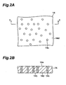
- Fig. 2A is a top view showing a part of the surface of the GaN substrate.
- Fig. 2B is a cross sectional view, taken along line I-I in Fig. 2A, showing the GaN substrate.
- This substrate 14 is manufactured as follows: A mask layer having a plurality of opening windows is formed on a GaAs substrate and GaN material is laterally grown on the GaAs substrate inside the opening windows of the mask layer. After the lateral growth, the GaAs substrate is removed off by aqua regalis etchant. The front and back surfaces 14a, 14b are mechanically polished to form the GaN substrate 14.
- the surface of the GaN substrate 14 has parts in which the density of threading dislocations is very high as compared to their surrounding area. As shown in Fig. 2B, the GaN substrate 14 has high dislocation regions 14c which extend in the Z direction. The low dislocation region 14d surrounds each of the high dislocation regions 14c that have the density of threading dislocations extremely higher than that of the low dislocation region 14d. The surface of the GaN substrate is dotted with the tops of the high dislocation regions 14c. The average density of threading dislocations in the high dislocation regions 14c is ten times as high as that in the low dislocation region 14d.
- GaN substrates in the present embodiment are made from a thick GaN layer formed by lateral growth; in the lateral growth, a number of depressed areas, such as pits each constituted by a plurality of facets, are formed on the surface of the thick GaN layer. Threading dislocations and other defects in the growing GaN layer of the present embodiment tend to gather as the thick GaN layer grows, resulting in forming the high dislocation regions in which the density of the above dislocations is high. The threading dislocations in the high dislocation regions form pits at the surface of the GaN substrate. The pits appear in island-shaped areas of the surface. The island-shaped areas are irregularly or randomly distributed over the surface of the substrate.
- the average density of the high dislocation regions 14c on the surface of the GaN substrate is not less than 100 per square centimeters (cm -2 ) .
- the high dislocation regions 14c and the low dislocation region 14d appear at the surface of the GaN substrate to form high dislocation areas and a low dislocation area, respectively.
- the ratio of the total dimension of the high dislocation areas to the dimension of the whole surface of the substrate is equal to or less than one percent.
- the average density of threading dislocations in the high dislocation areas is equal to or less than 3 ⁇ 10 7 per square centimeters (cm -2 ) and equal to or more than 1 ⁇ 10 6 per square centimeters (cm -2 ), and the average density of threading dislocations in the low dislocation area is equal to or less than 5 ⁇ 10 6 per square centimeters (cm -2 ).
- the average density of threading dislocations in the high dislocation areas is greater than the average density of threading dislocations in the low dislocation area.
- the size of the GaN substrate is not less than one inch.
- FIGS. 3A, 3B and 3C are cross sectional views showing the procedure of fabricating the GaN epitaxial substrate.
- a GaN single crystal substrate 14 is placed on the tray 20 on the susceptor 18 in the flow channel 12 as shown in Fig. 3A.
- the GaN substrate 14 has the upper surface 14a of (0001) face.
- a gas mixture containing NH 3 gas is supplied through the nozzles 22 to fill the flow channel 12 with the atmosphere of the gas mixture.
- the suspector 18 and substrate 14 are heated to about Celsius 1100 degrees (°C) by the heater 16 to carry out the process of cleaning the front surface 14a of the substrate 14 (thermal cleaning).
- the gas mixture is prepared by flowing NH 3 in the flow rate of 5 slm and H 2 in the flow rate of 6 slm. The thermal cleaning removes contaminants from the surface 14a of the substrate and improves the flatness of the substrate surface 14a.
- the temperature of the substrate 14 (substrate temperature) is kept at Celsius 1100 degrees (°C) and the pressure in the intermediate flow channel is kept at 80 kilopascals (kPa) or more, and the Group-III source gas, Group-V source gas and doping gas are supplied together with the carrier gas through the nozzles 22 onto the substrate 14 to grow an Al x Ga 1-x N intermediate layer 24 (intermediate layer forming step, Fig. 3B).
- TMG and TMA gases are supplied for 23 minutes in the condition of 24.42 micromoles per minute ( ⁇ mol/min) and 2.02 micromoles per minute ( ⁇ mol/min), respectively, and the flow rate of NH 3 and H 2 gases are 6 slm and 8 slm, respectively.
- the composition ratio x of aluminum can be within the range of 0 ⁇ x ⁇ 1.
- the thickness of the intermediate layer 24 can be within the range from 10 nanometers (nm) to 500 nanometers (nm) and can be changed by the growth conditions of the intermediate layer. The thickness of the intermediate layer 24 over the above range increases the possibility of occurrence of defects such as cracks.
- the inventors have found that defects such as cracks can be successfully suppressed if the thickness of the intermediate layer 24 is less than (-5x + 1.2) micrometers ( ⁇ m) in the composition ratio x of aluminum within the range of (0 ⁇ x ⁇ 0.24).
- the AlGaN intermediate layer 24 is formed on the GaN single crystal substrate 14 to form an epitaxial substrate, and the AlGaN intermediate layer 24 grows over the entire surface 14a, i.e., both the high dislocation areas and low dislocation area.
- the AlGaN intermediate layer 24 grows over the entire surface 14a, i.e., both the high dislocation areas and low dislocation area.
- a GaN layer is directly grown on the substrate 14, normal epitaxial growth does not occur on parts of the substrate surface 14a to form pits (as shown in Figs. 13 and 14), which must seriously damage the flatness of the surface of the GaN epitaxial substrate.
- the Inventors have conducted elaborate research and have found that depositing an AlGaN layer (intermediate layer 24) on the substrate 14 is effective in obtaining the desired flatness thereof.
- the intermediate layer 24 of AlGaN grows over the contaminated areas in the surface of the substrate and over the high dislocation regions 14c, and the surface 24a of the intermediate layer 24 is made flat and exhibits a good morphology.
- carbon is introduced into the intermediate layer 24, but the concentration of carbon is low, approximately not more than 1 ⁇ 10 18 cm -3 .
- the concentration of carbon may be approximately not less than 1 ⁇ 10 13 cm -3 .
- the substrate temperature is increased to Celsius 1150 degrees (°C) and a GaN upper layer 26 is epitaxially grown under a pressure of not less than 80 kilopascals (kPa) (upper layer forming step), thereby completing the fabrication of a GaN epitaxial substrate 28, i.e., a GaN epitaxial wafer (as shown in Fig. 3C).
- the surface 24a of the intermediate layer 24 is made flat as described above, and thus the surface 26a of the upper layer 26 (i.e., the surface of the GaN epitaxial substrate 28) is also made flat because the upper layer 26 is epitaxially grown on the intermediate layer 24 with good crystallinity.
- a light emitting device fabricated using the GaN epitaxial substrate 28 includes electrodes 30 provided on the bottom surface 14b of the substrate 14 and on the surface 26a of the upper layer 26.
- the intermediate layer 24 is provided between the substrate 14 and the upper layer 26 in the GaN epitaxial substrate 28.
- the Al x Ga 1-x N intermediate layer 24 is normally grown on the substrate 14 and its surface 24a created by the growth becomes flat. Since the upper layer 26 is epitaxially grown on the flat surface 24a of the intermediate layer 24, the surface 26a is also made flat.
- SiH 4 gas is diluted in 10 ppm with H 2 and the diluted SiH 4 gas is flown as dopant in the flow rate of 2.5 sccm in the step of forming the intermediate layer 24, whereby the intermediate layer 24 have an n-type conductivity in the carrier density of 5 ⁇ 10 18 cm -3 .
- Cp 2 Mg is flown as dopant in the condition of 0.0539 micromoles per minute ( ⁇ mol/min) in the step of forming the intermediate layer 24, the intermediate layer 24 has a p-type conductivity in the carrier density of 5 ⁇ 10 17 cm -3 .
- the GaN epitaxial substrate 28 includes the intermediate layer 24 with decreased resistivity, the GaN epitaxial substrate 28 is useful for fabricating a vertical structure device, such as light emitting diode (LED) or heterojunction bipolar transistor (HBT), both having improved device characteristics.
- LED light emitting diode
- HBT heterojunction bipolar transistor
- the intermediate layer 24 and upper layer 26 under the pressure of not less than 80 kilopascals (kPa). Since AlGaN material can be grown over the entire surface 14a of the substrate 14 as explained above, the growth surface 24a of the intermediate layer 24 can be made flat even if the intermediate layer 24 is grown under the relatively high pressure of not less than 80 kilopascals (kPa). Accordingly, by growing the intermediate layer 24 and the upper layer 26 under such a relatively high pressure, it is feasible to obtain the intermediate layer 24 and upper layer 26 both having good crystallinity.
- the average density of the high dislocation regions 14c may be equal to or more than 100 per square centimeters (cm -2 ). Even when the average density of the high dislocation regions 14c at the surface 14a is as high as the above value, the AlGaN intermediate layer improves the flatness of the surface thereof, and further improves the flatness of the surface of the upper layer 26.
- FIG. 4A, 4B, 4C, 4D and 4E another GaN epitaxial substrate and a method of fabricating the same will be described below.
- the other GaN substrate is different from the above-described epitaxial substrate.
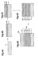
- Figs. 4A to 4E are views showing the procedure of fabricating the other GaN epitaxial substrate.
- an intermediate layer 24 is deposited on a substrate 14 by a method similar to that of fabricating the above-described GaN epitaxial substrate 28.
- the substrate 14 is placed in the tray 20 of the apparatus 10, and the substrate 14 has the top surface 14a of (0001) face.
- the above control of the switching valves is repeated to alternately deposit other intermediate layers 24A and epitaxial thin films 32 on the first epitaxial thin film 32 (Fig. 4D) so as to form a superlattice structure having, for example, five layers.
- an upper layer 26 is epitaxially grown on the uppermost intermediate layer 24A to fabricate the GaN epitaxial substrate 28A different from the aforementioned GaN epitaxial substrate 28.
- the material of the epitaxial thin films 32 is not limited to GaN material and can be selected from Al y Ga 1-y N (0 ⁇ y ⁇ 1) of compositions different from that of the intermediate layers 24A.
- the number of layers in the superlattice structure including the intermediate layers 24A and epitaxial thin films 32 is not limited to five, but the number of layers may be increased or decreased according to need.
- FIG. 5A, 5B, 5C, 5D and 5E another GaN epitaxial substrate and a method of fabricating the same will be described below.
- the other GaN epitaxial substrate of this modification is different from the above-described GaN epitaxial substrate and a method of fabricating a GaN epitaxial substrate.
- Figs. 5A to 5E are views showing the procedure of fabricating the other GaN substrate.
- An intermediate layer 24 is deposited on a substrate 14 by a method similar to the above-described method of fabricating the GaN epitaxial substrate 28.
- the substrate 14 is placed in the tray 20 of the apparatus 10, and the substrate 14 has the top surface 14a of the (0001) surface.
- the substrate 14 is subjected to a cleaning process (Fig. 5A).
- TMG is supplied for 11.5 minutes in 24.42 micromoles per minute ( ⁇ mol/min) and TMA is supplied in 2.02 micromoles per minute ( ⁇ mol/min), under the conditions of the substrate temperature of Celsius 1100 degrees (°C) and the pressure of not less than 80 kilopascals (kPa).
- NH 3 and H 2 gases are flown in the conditions of 6 slm and 8 slm, respectively.
- an AlGaN used as the intermediate layer may be abnormally grown on the substrate 14 as shown in Fig. 5B because of various reasons, such as an abnormal epitaxial growth, and the AlGaN intermediate layer does not have a desired surface flatness.
- an InGaN epitaxial layer is grown on this intermediate layer 24B.
- the Inventors have found that even when the substrate surface 14a is heavily contaminated and the density of the high dislocation regions 34 is high sufficient to cause abnormal growth of the intermediate layer 24B and to fail to achieve satisfactory flatness of the intermediate layer 24B, the InGaN layer 34 grown on the intermediate layer 24B provides the surface 34a that has flatness superior to that of the intermediate layer 24B.
- an intermediate layer 24C can be grown on the InGaN epitaxial layer 34 under a condition similar or equal to those for the intermediate layer 24B (Fig. 5D) and an upper layer 26 can be epitaxially grown on the intermediate layer 24C under conditions similar to those for the aforementioned upper layer to complete the GaN epitaxial substrate 28B (Fig. 4E). Since the intermediate layer 24C is grown on the InGaN epitaxial layer 34, the intermediate layer 24C prevents the surface of the InGaN epitaxial layer 34 from decomposing into constituent atoms at the increased substrate temperature during the formation of the upper layer 26.
- GaN epitaxial substrate 28B having the InGaN epitaxial layer 34 provided between the intermediate layers 24B and 24C even when satisfactory surface flatness is not achieved because of abnormal growth of the intermediate layer 24B, the combination of the InGaN epitaxial layer 34 and the intermediate layer 24C makes the flatness of the top surface 26a of the GaN epitaxial substrate 28B better. It is also possible to form the aforementioned superlattice structure by changing the aluminum concentration of the intermediate layers 24B and 24C and the indium concentration of the InGaN epitaxial layer 34. As required, GaN thin films may be provided between the intermediate layer 24B and 24C and the InGaN epitaxial layer 34. These GaN thin films are effective in alleviating strain induced by the lattice mismatch between AlGaN and InGaN.
- Fig. 6 is a cross sectional view showing a nitride semiconductor light emitting device 1A according to the present embodiment.
- a blue LED is exemplified as the light emitting device 1A.
- the light emitting device 1A includes an electrically conductive substrate 46, such as supporting body, made of a GaN single crystal and having a primary surface 46a and a back surface 46b.
- the GaN substrate 46 has high dislocation regions 14c which extend in the Z direction as in the GaN substrate 14.
- the surface of the GaN substrate 46 has areas in which the high dislocation regions 14c appear and in which the density of threading dislocations is very high as compared to its neighbor area.
- the surface of the GaN substrate is dotted with the high dislocation regions 14c.
- the average density of threading dislocations in the high dislocation regions 14c is ten times as high as that in the low dislocation region 14d.
- the low dislocation region 14d surrounds each of the high dislocation regions 14c that have the density of threading dislocations extremely higher than that of the low dislocation region 14d.
- the high dislocation regions 14c appear in the island-shaped areas of the surface 46a and are irregularly or randomly distributed over the surface 46a of the substrate 46.
- the density of the high dislocation regions, the threading dislocation densities of the high dislocation regions 14c and the low dislocation region 14d, the ratio of the total dimension of the high dislocation areas to the dimension of the whole surface of the substrate 46 are described above.
- the light emitting device 1A also has an intermediate layer 48, an n-type nitride semiconductor region 53, a light emitting layer 52, and a p-type nitride semiconductor region 55 which are epitaxially grown sequentially on the primary surface 46a of the substrate 46.
- the light emitting device 1A has a cathode electrode 58A provided on the back surface 46b of the substrate 46 and an anode electrode 58B provided on the p-type nitride semiconductor region 55.
- the cathode electrode 58A is provided on both the high dislocation regions 14c and the low dislocation region 14d to supply the first carries thereto
- the anode electrode 58B is provided on both the high dislocation regions 14c and the low dislocation region 14d to supply the second carries thereto.
- Some of the high dislocation regions 14c are provided between the cathode electrode 58A and the anode electrode 58B.
- the first and second carriers are recombined in the region 52a.
- the intermediate layer 48 includes an Al x Ga 1-x N (0 ⁇ x ⁇ 1) layer epitaxially grown on the primary surface 46a (e.g., the (0001) face) of the substrate 46.
- the intermediate layer 48 is doped with an n-type dopant.
- the intermediate layer 48 has the thickness of 50 nanometers (nm).
- the thickness of the intermediate layer 48 falls within the range of not less than 10 nanometers (nm) and not more than 500 nanometers (nm) and the desired thickness in this range can be realized by changing growth conditions for the intermediate layer 48.
- the thickness of the intermediate layer 48 over this range increases the possibility of occurrence of defects such as cracks.
- the thickness of the intermediate layer 48 is less than (-5x + 1.2) micrometers ( ⁇ m) where the composition ratio x of aluminum is 0 ⁇ x ⁇ 0.24, the occurrence of defects such as cracks can be well suppressed.
- the intermediate layer 48 inevitably contain carbon introduced during the process of the formation thereof, but the carbon concentration is at a level which does not degrade electric characteristics of the light emitting device 1A (1 ⁇ 10 18 cm -3 or less).
- the n-type nitride semiconductor region 53 includes a layer of an n-type nitride semiconductor, for example, such as an n-type buffer layer 50.
- the n-type buffer layer 50 is used as an upper layer in the present embodiment.
- the substrate 46, intermediate layer 48, and n-type buffer layer 50 in the present embodiment can be formed by cutting the GaN substrate 28 in the first embodiment into semiconductor dies.
- the n-type buffer layer 50 is formed by epitaxially growing GaN on the intermediate layer 48 and is doped with an n-type dopant, such as silicon (Si), to have the n-type conductivity.
- the n-type buffer layer 50 has such a composition as to have a refractive index smaller than that of the light emitting layer 52 and a bandgap larger than that of the light emitting layer 52.
- the n-type buffer layer 50 functions as a lower cladding layer for the light emitting layer 52.
- the n-type buffer layer 50 has the thickness of 2 micrometers ( ⁇ m).
- the light emitting layer 52 is formed on the n-type nitride semiconductor region 53 (on the n-type buffer layer 50 in the present embodiment). Carriers (electrons and holes) are fed thereto from the n-type nitride semiconductor region 53 and the p-type nitride semiconductor region 55 and are recombined to generate light therein.
- the light emitting layer 52 in the present embodiment has a multiple quantum well structure including barrier layers and well layers which are alternately stacked. In one example, each of the well layers has the thickness of 3 nanometers (nm) and each of the three barrier layers has the thickness of 15 nanometers (nm).
- the barrier layers and well layers each is made from InGaN in the present example.
- the bandgap of the barrier layers is larger than that of the well layers by differentiating the composition ratios of indium (In) in the barrier and well layers from each other.
- the p-type nitride semiconductor region 55 includes a layer of p-type nitride semiconductor, such as a p-type cladding layer 54 and a p-type contact layer 56.
- the p-type cladding layer 54 is formed by epitaxially growing AlGaN on the light emitting layer 52, and is doped with a p-type dopant, such as Mg, and has the p-type conductivity.
- the p-type cladding layer 54 has such a composition as to have a refractive index smaller than that of the light emitting layer 52 and a bandgap larger than that of the light emitting layer 52, and functions as an upper cladding layer for the light emitting layer 52.
- the p-type cladding layer 54 has the thickness of 20 nanometers (nm).
- the p-type contact layer 56 electrically connects the p-type cladding layer 54 to the anode electrode 58B.
- the p-type contact layer 56 is formed by epitaxially growing GaN on the p-type cladding layer 54 and is doped with a p-type dopant, e.g., Mg, and has the p-type conductivity.
- the p-type contact layer 56 has the thickness of 150 nanometers (nm).
- the cathode electrode 58A is made of an electrically conductive material that can achieve ohmic contact with the substrate 46.
- the anode electrode 58B is made of the electrically conductive material that achieves ohmic contact with the p-type nitride semiconductor region 55 (specifically, the p-type contact layer 56 in the present embodiment).
- the anode electrode 58B transmits light generated by the light emitting layer 52. At least a part of the anode electrode 58B may make the ohmic contact.
- FIGs. 7A, 7B, 7C, 7D and 7E are views showing the procedure of fabricating the light emitting device 1A.
- the GaN epitaxial substrate 28 in the first embodiment is prepared. Specifically, a GaN single crystal substrate 14 is placed in the tray 20 on the susceptor 18 in the flow channel 12 as shown in Fig. 1 (Fig. 7A). Then, the cleaning process (thermal cleaning) is carried out for the primary surface 14a of the substrate 14 in the same manner as in the first embodiment.
- the temperature of the substrate 14 (substrate temperature) is kept at Celsius 1050 degrees (°C) and the pressure is kept in the intermediate flow channel at 101 kilopascals (kPa).
- the Group-III source gas, Group-V source gas and dopant gas are supplied together with the aforementioned carrier gas through the nozzles 22 onto the substrate 14.
- TMG, TMA, NH 3 and SiH 4 gases are supplied onto the substrate 14 to grow an intermediate layer 24 of n-type AlGaN on the primary surface 14a of the substrate 14 (intermediate layer forming step, Fig. 7B).
- the growth conditions are preferably adjusted so that the composition of the intermediate layer 24 becomes Al x Ga 1-x N (0 ⁇ x ⁇ 0.24).
- the time period for the growth is chosen so that the thickness of the intermediate layer 24 becomes less than (-5x + 1.2) micrometers ( ⁇ m).
- TMG, NH 3 , and SiH 4 gases are supplied onto the intermediate layer 24 to epitaxially grow an n-type buffer layer, such as an n-type GaN upper layer 26, on the intermediate layer 24, and the substrate temperature and the pressure in the intermediate flow channel are maintained at Celsius 1050 degrees (°C) and at 101 kilopascals (kPa), respectively (Fig. 7C).
- the GaN epitaxial substrate 28 including the substrate 14, intermediate layer 24 and upper layer 26 is obtained.
- the substrate temperature is decreased to Celsius 800 degrees (°C), and TMG, TMI, and NH 3 gases are supplied onto the upper layer 26 to epitaxially grow a light emitting layer 66 of InGaN thereon.
- a quantum well structure is formed by periodically changing the flow rates of TMG, TMI, and NH 3 or the like to form barrier layers and well layers.
- the substrate temperature is increased to Celsius 1000 degrees (°C), and TMG, TMA, NH 3 and Cp 2 Mg gases are supplied onto the light emitting layer 66 to epitaxially grow a p-type cladding layer 68 of AlGaN on the light emitting layer 66.
- the substrate temperature is kept to Celsius 1000 degrees (°C)
- TMG, NH 3 , and Cp 2 Mg gases are supplied onto the p-type cladding layer 68 to epitaxially grow a p-type contact layer 70 of GaN on the p-type cladding layer 68 (semiconductor region forming step as shown in Fig. 7D).
- the GaN epitaxial substrate 28 including the light emitting layer 66, the p-type cladding layer 68 and the p-type contact layer 70 is taken out of the flow channel 12.
- the film 58A for cathode electrodes is formed on the back surface of the GaN substrate 28 by vapor deposition or the like, and the film 58B for anode electrodes is formed on the p-type contact layer 70 by vapor deposition or the like.
- the GaN epitaxial substrate 28 is divided into device units of a chip shape, i.e., semiconductor dies, to complete the light emitting device 1A that has the substrate 46, the intermediate layer 48, the n-type buffer layer 50, the light emitting layer 52, the p-type cladding layer 54 and the p-type contact layer 56 (Fig. 7E).
- the light emitting device 1A and the production method thereof according to the present embodiment as above will be described below.
- the uniform epitaxial growth of the GaN layer does not occur on parts of the surface of the substrate to form pits on the surfaces (Figs. 14 and 15), resulting in the poor flatness of the surface of the intermediate layer.
- the light emitting device 1A according to the present embodiment includes the intermediate AlGaN layer 24 (48) on the substrate 14 (46) and the fabrication method thereof includes the step of forming the intermediate layer 24 (48) of AlGaN on the substrate 14 (46).
- the surface 48a of the intermediate layer 48 can be made flat. Therefore, if one or more layers are deposited on the intermediate layer 48, the interfaces (growth surface) of these layers can be made flat, whereby the device characteristics, such as the emission amount of the light emitting device 1A, can be improved.
- the surface 48a of the intermediate layer 48 can be made flat because AlGaN grows over the entire surface 14a (46a), i.e., on the tops of the high dislocation regions and on areas of which contaminants are acquired.
- the n-type buffer layer 50, the light emitting layer 52, the p-type cladding layer 54 and the p-type contact layer 56 are grown on the intermediate layer 48 under such relatively high pressure and their interface can be made flat. Since these layers can be grown under the relatively high pressure, the crystallinity thereof can be made better. Accordingly, the device characteristics of the nitride semiconductor device are improved.
- the n-type nitride semiconductor region 53 include the n-type buffer layer 50 of GaN epitaxially grown on the intermediate layer 48 in the present embodiment.
- the growth surface (the surface of the n-type buffer layer 50) can be made flat by epitaxially growing the n-type buffer layer 50 on the intermediate layer 48. Therefore, the crystallinity of one or more layers epitaxially grown on the n-type buffer layer 50 is also improved and the device characteristics, such as the emission amount, in the light emitting device 1A are made excellent.
- the intermediate layer 48 be doped with an n-type dopant to have the n-type conductivity.
- the doping lowers the resistivity of the intermediate layer 48, so that the device characteristics, such as the emission amount, are made excellent in the light emitting device 1A, e.g., a vertical type light emitting device in which the substrate 46 is provided between the cathode electrode 58A and the anode electrode 58B.
- the intermediate layer 48 is doped with an n-type dopant, but it may be doped with a p-type dopant, depending upon the structure of light emitting device.
- the density of the high dislocation regions is equal to or more than 100 cm -2 at the surface of the substrate 46 as in the substrate 14. According to the light emitting device 1A and the fabrication method of the present invention, the surfaces of the intermediate layer 48 and semiconductor layers formed thereon can be made flat.
- a light generating region 52a in the light emitting layer 52 is provided on ones of the high dislocation regions 46c.
- the crystallinity of the light emitting layer 52 (particularly to the light generating region 52a) should be made excellent. Without the present embodiments, it has been hard to grow a light emitting layer having an excellent crystallinity on the high dislocation regions 14c, thereby preventing the fabrication of high-intensity light emitting devices. On the contrary, since the surface of the light emitting layer 52 of the light emitting device 1A can be made flat independent of the arrangement of the high dislocation regions 14c in the substrate 46, the crystallinity of the light generating region 52a becomes excellent.
- the light generating region 52a is provided between the cathode electrode 58A and the anode electrode 58B, and generates light in response to the supply of carries through the supply surfaces of the cathode electrode 58A and anode electrode 58B.
- the supply surfaces of the cathode electrode 58A and anode electrode 58B contact with semiconductor regions of the light emitting device 1A.
- Some of the high dislocation regions 14c are located between the cathode electrode 58A and the anode electrode 58B.
- the intermediate layer 48 in the present embodiment is different from so-called cladding layers.
- the thickness of the cladding layer should be relatively large in order to confine light to the light emitting layer.
- the n-type buffer layer 50 in the present embodiment has the thickness of 2 micrometers ( ⁇ m).
- the intermediate layer 48 in one example of the present embodiment has the thickness of 50 nanometers (nm). Even in such relatively small thickness, the intermediate layer 48 can have the technical effects as mentioned above.
- Fig. 8 is a cross sectional view showing the light emitting device 1B.
- the light emitting device 1B is different from the light emitting device 1A in the structure of the intermediate layer 49.
- the structure of the light emitting device 1B is similar to that of the aforementioned light emitting device 1A except an intermediate layer 49 in the light emitting device 1B, and thus the detailed description will be omitted except for the description of the intermediate layer 49.
- the light emitting device 1B has the intermediate layer 49 provided on the surface 46a of the substrate 46.
- the intermediate layer 49 is constituted by first layers 49A and second layers 49B, and the first layers 49A and the second layers 49B are deposited alternately.
- the first layers 49A are made of Al x Ga 1-x N (0 ⁇ x ⁇ 1) doped with an n-type dopant
- the second layers 49B of Al y Ga 1-y N (0 ⁇ y ⁇ 1, y ⁇ x) doped with an n-type dopant.
- the first layers 49A and second layers 49B are alternately arranged on the surface 46a of the substrate 46 to constitute a superlattice structure (strained superlattice structure), and the number of the first and second layers 49A and 49B in the superlattice structure is, for example, ten.
- the first layers 49A and the second layers 49B each have the thickness, for example, of 10 nanometers (nm).
- the superlattice structure prevents threading dislocations from extending from the substrate 46.
- the superlattice structure reduces the dislocation densities of the n-type nitride semiconductor region 53, light emitting layer 52 and p-type nitride semiconductor region 55 to improve their crystallinity, whereby the device characteristics, such as emission luminance, can be made excellent.
- the superlattice structure including the first layers 49A and the second layers 49B should not be limited to the ten-layer structure as above, but the number of layers may be changed as required.
- Fig. 9 is a cross sectional view showing the light emitting device 1C.
- the light emitting device 1C is different from the light emitting devices 1A and 1B in that the light emitting device 1C has an InGaN epitaxial layer 57 between intermediate layers 51A and 51B.
- the structure of the light emitting device 1C is similar to those of the aforementioned light emitting devices 1A and 1B except that the light emitting device 1C has the InGaN epitaxial layer 57, and the detailed description will be omitted except for the description of the InGaN epitaxial layer 57.
- the light emitting device 1C has intermediate layers 51 provided on the surface 46a of the substrate 46.
- the intermediate layers 51 are constituted by the first layer 51A and the second layer 51B.
- the light emitting device 1C has an InGaN epitaxial layer 57 provided between the first layer 51A and the second layer 51B of the intermediate layers 51.
- Each of the first layer 51A and the second layer 51B is made of Al x Ga 1-x N (0 ⁇ x ⁇ 1) doped with a n-type dopant
- the InGaN epitaxial layer 57 is made of In z Ga 1-z N (0 ⁇ z ⁇ 1) doped with a n-type dopant.
- a method of fabricating the light emitting device 1C is similar to that of the light emitting device 1A except for the following: in the step of forming the intermediate layers 51 of the light emitting device 1C, TMG, TMI, NH 3 and SiH 4 gases are supplied onto the first layer 51A to grow the InGaN epitaxial layer 57 of n-type In z Ga 1-z N (0 ⁇ z ⁇ 1) after forming the first layer 51A of n-type AlGaN. Then, an n-type AlGaN is grown on the InGaN epitaxial layer 57 to form the second layer 51B.
- the first layer 51A has been formed as a result of an abnormal growth.
- An abnormal growth of semiconductor layers may occur on the substrate 46 for various reasons even if a layer of AlGaN may be deposited thereon.
- the epitaxial layer 57 of In z Ga 1-z N (0 ⁇ z ⁇ 1) is grown on the first layer 51A.
- the layer of InGaN is deposited on the first layer 51A to obtain the flat surface 57a as compared to that of the first layer 51A.
- a blue light emitting device 1A is fabricated as a first example.
- the substrate 14 of a GaN single crystal like a wafer is placed in the tray 20 on the susceptor 18.
- the pressure in the flow channel 12 pressure in a furnace
- NH 3 and H 2 gases are supplied to the flow channel 12 and the temperature of the substrate 14 is maintained at Celsius 1050 degrees (°C) for ten minutes to clean the surface 60a.
- the substrate temperature and the furnace pressure are kept at Celsius 1050 degrees (°C) and 101 kilopascals (kPa), respectively, and TMA, TMG, NH 3 , and SiH 4 gases are supplied to the flow channel 12 to grow the intermediate layer 24, for example, an n-type Al 0.07 Ga 0.93 N layer in the thickness of 50 nanometers (nm).
- the substrate temperature and the furnace pressure are kept unchanged, and the upper layer 26 is grown as the n-type GaN buffer layer 50 in the thickness of 2 micrometers ( ⁇ m), thereby obtaining the GaN epitaxial substrate 28.
- the substrate temperature is decreased to Celsius 800 degrees (°C), and InGaN barrier layers of 15 nanometer thickness and InGaN well layers of 3 nanometer thickness are alternately grown over three cycles, thus forming a light emitting layer 66.
- the substrate temperature is again increased to Celsius 1000 degrees (°C), and TMA, TMG, NH 3 and Cp 2 Mg gases are supplied to the flow channel 12 to grow a p-type cladding layer of Al 0.12 Ga 0.88 N in the thickness of 20 nanometers (nm).
- TMG, NH 3 and Cp 2 Mg gases are supplied to grow a p-type contact layer of GaN in the thickness of 50 nanometers (nm).
- Fig. 10 is a view showing the surface of the p-type contact layer in the light emitting device 1A fabricated as the present example. This is a photograph taken with a differential interference microscope. It is seen from Fig. 10 that the surface of the p-type contact layer is flat with little unevenness. The surface of the p-type contact layer of the uppermost layer reflects flatness of the interfaces (growth surfaces) of lower layers, such as the p-type cladding layer, light emitting layer and upper layer, and thus we can expect from the photograph shown in Fig. 10 that the interfaces of the p-type cladding layer 68, light emitting layer 66, and upper layer 26 are also flat.
- the cathode electrode 58A is formed on the back surface of the GaN epitaxial substrate 28, and the anode electrode 58B is formed on the p-type contact layer.
- the GaN epitaxial substrate 28 is divided into semiconductor dies to complete light emitting devices, such as the light emitting device 1A.
- the wavelength of emission is 450 nanometers (nm) at 20 milliamperes (mA) and the power of emission is 3 milliwatts (mW).
- Fig. 11A shows a summary representing the results of investigation on presence/absence of cracks, for each of the intermediate layers 48 prepared in thirteen levels of thickness values and aluminum composition ratios. The summary also presents the thickness values of the intermediate layers 48, and the aluminum composition ratios x derived from PL wavelength.
- a blue light emitting device 1B has been fabricated as a second example.
- the substrate 14 is placed in the tray 20 and the surface 14a thereof is cleaned in the same manner as in the first example.
- the substrate temperature and the furnace pressure is kept at Celsius 1050 degrees (°C) and at 101 kilopascals (kPa), respectively, and TMA, TMG, NH 3 and SiH 4 gases are supplied to the flow channel 12 to alternately deposit ten cycles of n-type Al 0.14 Ga 0.86 N layers in the thickness of 10 nanometers (nm) and n-type GaN layers in the thickness of 10 nanometers (nm), thereby growing an intermediate layer.
- an n-type buffer layer, a light emitting layer, a p-type cladding layer and a p-type contact layer are grown in the same manner as that in the first example.
- the surface of the p-type contact layer grown as above is observed with a differential interference microscope and this photograph reveals that the surface of the p-type contact layer is made flat as in the first example.
- the cathode electrode 58A is formed on the back surface of the substrate 14 and the anode electrode 58B is formed on the p-type contact layer. Then, the substrate 14 is divided into semiconductor dies to complete light emitting devices, such as the light emitting device 1B.
- the wavelength of emission is 450 nanometers (nm) at 20 milliamperes (mA) and the power of emission is 5 milliwatts (mW).
- a GaN single crystal substrate is placed in the tray 20 on the susceptor 18 and the surface thereof is cleaned in the same manner as in the first example. Then, while keeping the substrate temperature at Celsius 1050 degrees (°C) and the furnace pressure at 101 kilopascals (kPa), TMG, NH 3 and SiH 4 are supplied the flow channel 12 to grow n-type GaN in the thickness of 2 micrometers ( ⁇ m). Thereafter, a light emitting layer, a p-type cladding layer, and a p-type contact layer are successively grown in the same manner as in the first example.
- Fig. 12 is a view showing the surface of the p-type contact layer in the light emitting device fabricated as the experiment example. This is a photograph taken with a differential interference microscope. As shown in Fig. 12, the surface of the p-type contact layer in this example is considerably uneven and the flatness thereof is not good. Therefore, we can presume that the interfaces of the p-type cladding layer, light emitting layer, and n-type buffer layer also have poor flatness.
- the cathode electrode is formed on the back surface of the substrate and the anode electrode is formed on the p-type contact layer.
- the substrate is divided into semiconductor dies to complete light emitting devices.
- Current is continuously applied to a bare chip of a light emitting device fabricated as above, and the wavelength of emission is 450 nanometers (nm) at the current of 20 milliamperes (mA) and the power of emission is only 1 milliwatts (mW). This proves that the intermediate layer provided on the substrate is effective in improving the device characteristics of the light emitting devices or the like as in each of the above examples.
- the present invention is not limited to the above embodiments and examples, but can be modified in various ways.
- the n-type semiconductor region is formed on the intermediate layer and the p-type semiconductor region is formed on the active layer, but it is also possible that the p-type semiconductor region is formed on the intermediate layer and that the n-type semiconductor region is formed on the active layer.
- the second embodiment exemplifies the light emitting devices as nitride semiconductor devices of the present invention, but the present invention is not limited thereto and can also be suitably applied to transistors and others made of GaN based material having the n-type region and p-type region.
Landscapes
- Chemical & Material Sciences (AREA)
- Engineering & Computer Science (AREA)
- Crystallography & Structural Chemistry (AREA)
- Materials Engineering (AREA)
- Metallurgy (AREA)
- Organic Chemistry (AREA)
- Chemical Kinetics & Catalysis (AREA)
- General Chemical & Material Sciences (AREA)
- Inorganic Chemistry (AREA)
- Led Devices (AREA)
- Crystals, And After-Treatments Of Crystals (AREA)
Applications Claiming Priority (4)
| Application Number | Priority Date | Filing Date | Title |
|---|---|---|---|
| JP2003183173 | 2003-06-26 | ||
| JP2003183173 | 2003-06-26 | ||
| JP2004173059 | 2004-06-10 | ||
| JP2004173059A JP4229005B2 (ja) | 2003-06-26 | 2004-06-10 | GaN基板及びその製造方法、並びに窒化物半導体素子 |
Publications (2)
| Publication Number | Publication Date |
|---|---|
| EP1492158A2 true EP1492158A2 (de) | 2004-12-29 |
| EP1492158A3 EP1492158A3 (de) | 2009-11-11 |
Family
ID=33422211
Family Applications (1)
| Application Number | Title | Priority Date | Filing Date |
|---|---|---|---|
| EP04014870A Withdrawn EP1492158A3 (de) | 2003-06-26 | 2004-06-24 | GaN-Substrat und dessen Herstelungsverfahren, nitrid-Halbleitervorrichtung und Herstellungsverfahren |
Country Status (6)
| Country | Link |
|---|---|
| US (1) | US7387678B2 (de) |
| EP (1) | EP1492158A3 (de) |
| JP (1) | JP4229005B2 (de) |
| KR (2) | KR101182019B1 (de) |
| CN (1) | CN100483627C (de) |
| TW (1) | TW200516649A (de) |
Cited By (3)
| Publication number | Priority date | Publication date | Assignee | Title |
|---|---|---|---|---|
| WO2006110203A1 (en) * | 2005-04-11 | 2006-10-19 | Cree, Inc. | Composite substrates of conductive and insulating or semi-insulating group iii-nitrides for group iii-nitride devices |
| CN101853909A (zh) * | 2009-03-30 | 2010-10-06 | 丰田合成株式会社 | Ⅲ族氮化物化合物半导体发光元件及其制造方法 |
| EP2767620A1 (de) * | 2013-02-15 | 2014-08-20 | Azzurro Semiconductors AG | P-doping einer Gruppe-III-Nitridpufferschichtstruktur auf einem Heterosubstrat |
Families Citing this family (74)
| Publication number | Priority date | Publication date | Assignee | Title |
|---|---|---|---|---|
| JP4052150B2 (ja) * | 2003-03-05 | 2008-02-27 | 住友電気工業株式会社 | 窒化物系半導体装置の製造方法 |
| US7508001B2 (en) * | 2004-06-21 | 2009-03-24 | Panasonic Corporation | Semiconductor laser device and manufacturing method thereof |
| JP4792814B2 (ja) * | 2005-05-26 | 2011-10-12 | 住友電気工業株式会社 | 高電子移動度トランジスタ、電界効果トランジスタ、エピタキシャル基板、エピタキシャル基板を作製する方法およびiii族窒化物系トランジスタを作製する方法 |
| US9331192B2 (en) | 2005-06-29 | 2016-05-03 | Cree, Inc. | Low dislocation density group III nitride layers on silicon carbide substrates and methods of making the same |
| JP5151139B2 (ja) * | 2006-12-19 | 2013-02-27 | 住友電気工業株式会社 | 半導体発光素子 |
| JP2008246604A (ja) * | 2007-03-29 | 2008-10-16 | Fujitsu Ltd | マイクロ可動素子、ウエハ、およびウエハ製造方法 |
| JP2008300541A (ja) * | 2007-05-30 | 2008-12-11 | Sumitomo Electric Ind Ltd | 半導体発光素子及びそれに用いる素子形成用基板 |
| KR100972974B1 (ko) * | 2007-12-17 | 2010-07-29 | 삼성엘이디 주식회사 | Ⅲ족 질화물 기판의 표면개선방법, 이로부터 제조된 ⅲ족질화물 기판 및 이러한 ⅲ족 질화물 기판을 이용한 질화물반도체 발광 소자 |
| US20090309127A1 (en) * | 2008-06-13 | 2009-12-17 | Soraa, Inc. | Selective area epitaxy growth method and structure |
| US8847249B2 (en) | 2008-06-16 | 2014-09-30 | Soraa, Inc. | Solid-state optical device having enhanced indium content in active regions |
| US8259769B1 (en) | 2008-07-14 | 2012-09-04 | Soraa, Inc. | Integrated total internal reflectors for high-gain laser diodes with high quality cleaved facets on nonpolar/semipolar GaN substrates |
| US8805134B1 (en) | 2012-02-17 | 2014-08-12 | Soraa Laser Diode, Inc. | Methods and apparatus for photonic integration in non-polar and semi-polar oriented wave-guided optical devices |
| US8837545B2 (en) | 2009-04-13 | 2014-09-16 | Soraa Laser Diode, Inc. | Optical device structure using GaN substrates and growth structures for laser applications |
| US8634442B1 (en) | 2009-04-13 | 2014-01-21 | Soraa Laser Diode, Inc. | Optical device structure using GaN substrates for laser applications |
| DE112010001615T5 (de) | 2009-04-13 | 2012-08-02 | Soraa, Inc. | Stuktur eines optischen Elements unter Verwendung von GaN-Substraten für Laseranwendungen |
| US10108079B2 (en) | 2009-05-29 | 2018-10-23 | Soraa Laser Diode, Inc. | Laser light source for a vehicle |
| US8509275B1 (en) | 2009-05-29 | 2013-08-13 | Soraa, Inc. | Gallium nitride based laser dazzling device and method |
| US8427590B2 (en) | 2009-05-29 | 2013-04-23 | Soraa, Inc. | Laser based display method and system |
| US9800017B1 (en) | 2009-05-29 | 2017-10-24 | Soraa Laser Diode, Inc. | Laser device and method for a vehicle |
| US9829780B2 (en) | 2009-05-29 | 2017-11-28 | Soraa Laser Diode, Inc. | Laser light source for a vehicle |
| US9250044B1 (en) | 2009-05-29 | 2016-02-02 | Soraa Laser Diode, Inc. | Gallium and nitrogen containing laser diode dazzling devices and methods of use |
| US8355418B2 (en) | 2009-09-17 | 2013-01-15 | Soraa, Inc. | Growth structures and method for forming laser diodes on {20-21} or off cut gallium and nitrogen containing substrates |
| US8750342B1 (en) | 2011-09-09 | 2014-06-10 | Soraa Laser Diode, Inc. | Laser diodes with scribe structures |
| US9927611B2 (en) | 2010-03-29 | 2018-03-27 | Soraa Laser Diode, Inc. | Wearable laser based display method and system |
| JP2012009783A (ja) * | 2010-06-28 | 2012-01-12 | Meijo Univ | Iii族窒化物系太陽電池 |
| US8816319B1 (en) | 2010-11-05 | 2014-08-26 | Soraa Laser Diode, Inc. | Method of strain engineering and related optical device using a gallium and nitrogen containing active region |
| GB2487531A (en) * | 2011-01-20 | 2012-08-01 | Sharp Kk | Substrate system consisting of a metamorphic transition region comprising a laminate of AlxGa1-x N and the same material as the substrate. |
| US9318875B1 (en) | 2011-01-24 | 2016-04-19 | Soraa Laser Diode, Inc. | Color converting element for laser diode |
| US9025635B2 (en) | 2011-01-24 | 2015-05-05 | Soraa Laser Diode, Inc. | Laser package having multiple emitters configured on a support member |
| US9595813B2 (en) | 2011-01-24 | 2017-03-14 | Soraa Laser Diode, Inc. | Laser package having multiple emitters configured on a substrate member |
| US9093820B1 (en) | 2011-01-25 | 2015-07-28 | Soraa Laser Diode, Inc. | Method and structure for laser devices using optical blocking regions |
| JP2011109136A (ja) * | 2011-02-22 | 2011-06-02 | Sumitomo Electric Ind Ltd | 窒化ガリウム系エピタキシャルウエハ、およびエピタキシャルウエハを作製する方法 |
| US9236530B2 (en) | 2011-04-01 | 2016-01-12 | Soraa, Inc. | Miscut bulk substrates |
| JP5533791B2 (ja) * | 2011-06-20 | 2014-06-25 | 豊田合成株式会社 | Iii族窒化物半導体発光素子の製造方法 |
| US9646827B1 (en) | 2011-08-23 | 2017-05-09 | Soraa, Inc. | Method for smoothing surface of a substrate containing gallium and nitrogen |
| JP2012074740A (ja) * | 2011-12-28 | 2012-04-12 | Sumitomo Electric Ind Ltd | 半導体発光素子 |
| CN104205297B (zh) * | 2012-03-21 | 2018-06-15 | 首尔伟傲世有限公司 | 制造非极性氮化镓基半导体层的方法、非极性半导体器件及其制造方法 |
| JP5641029B2 (ja) * | 2012-09-24 | 2014-12-17 | 住友電気工業株式会社 | Iii族窒化物系電子デバイス |
| US9166372B1 (en) | 2013-06-28 | 2015-10-20 | Soraa Laser Diode, Inc. | Gallium nitride containing laser device configured on a patterned substrate |
| US9379525B2 (en) | 2014-02-10 | 2016-06-28 | Soraa Laser Diode, Inc. | Manufacturable laser diode |
| US9368939B2 (en) | 2013-10-18 | 2016-06-14 | Soraa Laser Diode, Inc. | Manufacturable laser diode formed on C-plane gallium and nitrogen material |
| US9362715B2 (en) | 2014-02-10 | 2016-06-07 | Soraa Laser Diode, Inc | Method for manufacturing gallium and nitrogen bearing laser devices with improved usage of substrate material |
| US9520695B2 (en) | 2013-10-18 | 2016-12-13 | Soraa Laser Diode, Inc. | Gallium and nitrogen containing laser device having confinement region |
| US9209596B1 (en) | 2014-02-07 | 2015-12-08 | Soraa Laser Diode, Inc. | Manufacturing a laser diode device from a plurality of gallium and nitrogen containing substrates |
| US9871350B2 (en) | 2014-02-10 | 2018-01-16 | Soraa Laser Diode, Inc. | Manufacturable RGB laser diode source |
| US9520697B2 (en) | 2014-02-10 | 2016-12-13 | Soraa Laser Diode, Inc. | Manufacturable multi-emitter laser diode |
| US9564736B1 (en) * | 2014-06-26 | 2017-02-07 | Soraa Laser Diode, Inc. | Epitaxial growth of p-type cladding regions using nitrogen gas for a gallium and nitrogen containing laser diode |
| CN104201256B (zh) * | 2014-08-26 | 2017-09-26 | 中国科学院半导体研究所 | 低电阻率低温p型铝镓氮材料的制备方法 |
| CN104332545A (zh) * | 2014-09-02 | 2015-02-04 | 中国科学院半导体研究所 | 低电阻率p型铝镓氮材料及其制备方法 |
| US12126143B2 (en) | 2014-11-06 | 2024-10-22 | Kyocera Sld Laser, Inc. | Method of manufacture for an ultraviolet emitting optoelectronic device |
| US9246311B1 (en) | 2014-11-06 | 2016-01-26 | Soraa Laser Diode, Inc. | Method of manufacture for an ultraviolet laser diode |
| KR102291883B1 (ko) * | 2014-12-22 | 2021-08-20 | 주식회사 케이씨텍 | 화학 기계적 연마 공정이 행해진 웨이퍼의 처리 장치 |
| US9653642B1 (en) | 2014-12-23 | 2017-05-16 | Soraa Laser Diode, Inc. | Manufacturable RGB display based on thin film gallium and nitrogen containing light emitting diodes |
| US9666677B1 (en) | 2014-12-23 | 2017-05-30 | Soraa Laser Diode, Inc. | Manufacturable thin film gallium and nitrogen containing devices |
| US11437774B2 (en) | 2015-08-19 | 2022-09-06 | Kyocera Sld Laser, Inc. | High-luminous flux laser-based white light source |
| US11437775B2 (en) | 2015-08-19 | 2022-09-06 | Kyocera Sld Laser, Inc. | Integrated light source using a laser diode |
| US10879673B2 (en) | 2015-08-19 | 2020-12-29 | Soraa Laser Diode, Inc. | Integrated white light source using a laser diode and a phosphor in a surface mount device package |
| US10938182B2 (en) | 2015-08-19 | 2021-03-02 | Soraa Laser Diode, Inc. | Specialized integrated light source using a laser diode |
| US9787963B2 (en) | 2015-10-08 | 2017-10-10 | Soraa Laser Diode, Inc. | Laser lighting having selective resolution |
| CN106783533B (zh) * | 2016-11-11 | 2020-01-07 | 上海芯元基半导体科技有限公司 | 含Al氮化物半导体结构及其外延生长方法 |
| US10771155B2 (en) | 2017-09-28 | 2020-09-08 | Soraa Laser Diode, Inc. | Intelligent visible light with a gallium and nitrogen containing laser source |
| US10222474B1 (en) | 2017-12-13 | 2019-03-05 | Soraa Laser Diode, Inc. | Lidar systems including a gallium and nitrogen containing laser light source |
| US10551728B1 (en) | 2018-04-10 | 2020-02-04 | Soraa Laser Diode, Inc. | Structured phosphors for dynamic lighting |
| US11421843B2 (en) | 2018-12-21 | 2022-08-23 | Kyocera Sld Laser, Inc. | Fiber-delivered laser-induced dynamic light system |
| US11239637B2 (en) | 2018-12-21 | 2022-02-01 | Kyocera Sld Laser, Inc. | Fiber delivered laser induced white light system |
| US12000552B2 (en) | 2019-01-18 | 2024-06-04 | Kyocera Sld Laser, Inc. | Laser-based fiber-coupled white light system for a vehicle |
| US12152742B2 (en) | 2019-01-18 | 2024-11-26 | Kyocera Sld Laser, Inc. | Laser-based light guide-coupled wide-spectrum light system |
| US11884202B2 (en) | 2019-01-18 | 2024-01-30 | Kyocera Sld Laser, Inc. | Laser-based fiber-coupled white light system |
| WO2020213388A1 (ja) * | 2019-04-19 | 2020-10-22 | ソニー株式会社 | 化合物半導体層積層体及びその形成方法、並びに、発光デバイス |
| US11228158B2 (en) | 2019-05-14 | 2022-01-18 | Kyocera Sld Laser, Inc. | Manufacturable laser diodes on a large area gallium and nitrogen containing substrate |
| US10903623B2 (en) | 2019-05-14 | 2021-01-26 | Soraa Laser Diode, Inc. | Method and structure for manufacturable large area gallium and nitrogen containing substrate |
| US12191626B1 (en) | 2020-07-31 | 2025-01-07 | Kyocera Sld Laser, Inc. | Vertically emitting laser devices and chip-scale-package laser devices and laser-based, white light emitting devices |
| CN112397571B (zh) * | 2021-01-18 | 2021-04-23 | 苏州纳维科技有限公司 | 一种氮化镓衬底及半导体复合衬底 |
| CN120138791A (zh) * | 2023-12-12 | 2025-06-13 | 中微半导体设备(上海)股份有限公司 | 一种进气装置及气相沉积设备 |
Citations (1)
| Publication number | Priority date | Publication date | Assignee | Title |
|---|---|---|---|---|
| EP0993048A2 (de) * | 1998-09-14 | 2000-04-12 | Matsushita Electronics Corporation | Nitrid-Halbleitervorrichtung und ihr Herstellungsverfahren |
Family Cites Families (17)
| Publication number | Priority date | Publication date | Assignee | Title |
|---|---|---|---|---|
| JP3847000B2 (ja) | 1997-11-26 | 2006-11-15 | 日亜化学工業株式会社 | 窒化物半導体基板上に活性層を備えた窒化物半導体層を有する窒化物半導体素子及びその成長方法 |
| JP2000012979A (ja) | 1998-06-26 | 2000-01-14 | Nichia Chem Ind Ltd | 窒化物半導体基板の製造方法 |
| DE60043122D1 (de) * | 1999-03-17 | 2009-11-19 | Mitsubishi Chem Corp | Halbleiterbasis ihre Herstellung und Halbleiterkristallhersetllungsmethode |
| JP2000340509A (ja) | 1999-05-26 | 2000-12-08 | Sumitomo Electric Ind Ltd | GaN基板およびその製造方法 |
| JP4145437B2 (ja) | 1999-09-28 | 2008-09-03 | 住友電気工業株式会社 | 単結晶GaNの結晶成長方法及び単結晶GaN基板の製造方法と単結晶GaN基板 |
| EP1265273A4 (de) * | 2000-03-14 | 2009-05-06 | Toyoda Gosei Kk | Herstellungsverfahren für einen iii-nitridverbin-dungshalbleiter und iii-nitridverbindungshalb-leiterelement |
| TW518767B (en) * | 2000-03-31 | 2003-01-21 | Toyoda Gosei Kk | Production method of III nitride compound semiconductor and III nitride compound semiconductor element |
| JP2001313259A (ja) * | 2000-04-28 | 2001-11-09 | Toyoda Gosei Co Ltd | Iii族窒化物系化合物半導体基板の製造方法及び半導体素子 |
| JP2001326245A (ja) | 2000-05-16 | 2001-11-22 | Hitachi Ltd | 半導体装置およびその製造方法 |
| JP3968968B2 (ja) * | 2000-07-10 | 2007-08-29 | 住友電気工業株式会社 | 単結晶GaN基板の製造方法 |
| JP2002190635A (ja) | 2000-12-20 | 2002-07-05 | Sharp Corp | 半導体レーザ素子およびその製造方法 |
| JP3988018B2 (ja) * | 2001-01-18 | 2007-10-10 | ソニー株式会社 | 結晶膜、結晶基板および半導体装置 |
| JP3866540B2 (ja) * | 2001-07-06 | 2007-01-10 | 株式会社東芝 | 窒化物半導体素子およびその製造方法 |
| JP4948720B2 (ja) | 2001-08-29 | 2012-06-06 | シャープ株式会社 | 窒素化合物半導体積層物、発光素子、光ピックアップシステム、および窒素化合物半導体積層物の製造方法。 |
| JP4920152B2 (ja) | 2001-10-12 | 2012-04-18 | 住友電気工業株式会社 | 構造基板の製造方法および半導体素子の製造方法 |
| JP4290358B2 (ja) | 2001-10-12 | 2009-07-01 | 住友電気工業株式会社 | 半導体発光素子の製造方法 |
| JP2003229638A (ja) | 2002-02-05 | 2003-08-15 | Sumitomo Electric Ind Ltd | 窒化物系化合物半導体発光素子 |
-
2004
- 2004-06-10 JP JP2004173059A patent/JP4229005B2/ja not_active Expired - Fee Related
- 2004-06-24 EP EP04014870A patent/EP1492158A3/de not_active Withdrawn
- 2004-06-25 TW TW093118680A patent/TW200516649A/zh not_active IP Right Cessation
- 2004-06-25 KR KR1020040048173A patent/KR101182019B1/ko not_active Expired - Fee Related
- 2004-06-25 CN CNB2004100628322A patent/CN100483627C/zh not_active Expired - Fee Related
- 2004-06-25 US US10/875,512 patent/US7387678B2/en not_active Expired - Fee Related
-
2011
- 2011-02-21 KR KR1020110014950A patent/KR101188501B1/ko not_active Expired - Fee Related
Patent Citations (1)
| Publication number | Priority date | Publication date | Assignee | Title |
|---|---|---|---|---|
| EP0993048A2 (de) * | 1998-09-14 | 2000-04-12 | Matsushita Electronics Corporation | Nitrid-Halbleitervorrichtung und ihr Herstellungsverfahren |
Non-Patent Citations (1)
| Title |
|---|
| MOTOKI K ET AL: "Growth and characterization of freestanding GaN substrates", JOURNAL OF CRYSTAL GROWTH ELSEVIER NETHERLANDS, vol. 237-239, no. 2, April 2002 (2002-04-01), pages 912 - 921, XP004355910, ISSN: 0022-0248 * |
Cited By (11)
| Publication number | Priority date | Publication date | Assignee | Title |
|---|---|---|---|---|
| WO2006110203A1 (en) * | 2005-04-11 | 2006-10-19 | Cree, Inc. | Composite substrates of conductive and insulating or semi-insulating group iii-nitrides for group iii-nitride devices |
| US7626217B2 (en) | 2005-04-11 | 2009-12-01 | Cree, Inc. | Composite substrates of conductive and insulating or semi-insulating group III-nitrides for group III-nitride devices |
| CN101853909A (zh) * | 2009-03-30 | 2010-10-06 | 丰田合成株式会社 | Ⅲ族氮化物化合物半导体发光元件及其制造方法 |
| EP2767620A1 (de) * | 2013-02-15 | 2014-08-20 | Azzurro Semiconductors AG | P-doping einer Gruppe-III-Nitridpufferschichtstruktur auf einem Heterosubstrat |
| WO2014125092A1 (en) * | 2013-02-15 | 2014-08-21 | TARKOTTA, Gunter | P-doping of group-iii-nitride buffer layer structure on a heterosubstrate |
| US9496349B2 (en) | 2013-02-15 | 2016-11-15 | Azurspace Solar Power Gmbh | P-doping of group-III-nitride buffer layer structure on a heterosubstrate |
| US9786744B2 (en) | 2013-02-15 | 2017-10-10 | Azurspace Solar Power Gmbh | P-doping of group-III-nitride buffer layer structure on a heterosubstrate |
| EP3282041A1 (de) * | 2013-02-15 | 2018-02-14 | AZUR SPACE Solar Power GmbH | P-doping einer gruppe iii-nitridpufferschichtstruktur auf einem heterosubstrat |
| US10026814B2 (en) | 2013-02-15 | 2018-07-17 | Azurspace Solar Power Gmbh | P-doping of group-III-nitride buffer layer structure on a heterosubstrate |
| US10211296B2 (en) | 2013-02-15 | 2019-02-19 | Azurspace Solar Power Gmbh | P-doping of group-III-nitride buffer layer structure on a heterosubstrate |
| EP3708699A1 (de) * | 2013-02-15 | 2020-09-16 | AZUR SPACE Solar Power GmbH | P-doping einer gruppe iii-nitridpufferschichtstruktur auf einem heterosubstrat |
Also Published As
| Publication number | Publication date |
|---|---|
| KR101182019B1 (ko) | 2012-09-11 |
| JP2005039223A (ja) | 2005-02-10 |
| TW200516649A (en) | 2005-05-16 |
| KR20110025198A (ko) | 2011-03-09 |
| EP1492158A3 (de) | 2009-11-11 |
| KR20050001460A (ko) | 2005-01-06 |
| US7387678B2 (en) | 2008-06-17 |
| JP4229005B2 (ja) | 2009-02-25 |
| KR101188501B1 (ko) | 2012-10-08 |
| US20040262624A1 (en) | 2004-12-30 |
| CN100483627C (zh) | 2009-04-29 |
| TWI352378B (de) | 2011-11-11 |
| CN1577743A (zh) | 2005-02-09 |
Similar Documents
| Publication | Publication Date | Title |
|---|---|---|
| US7387678B2 (en) | GaN substrate and method of fabricating the same, nitride semiconductor device and method of fabricating the same | |
| US7084421B2 (en) | Light-emitting device using group III nitride group compound semiconductor | |
| KR100448662B1 (ko) | 질화물반도체소자 및 그 제조방법 | |
| US5998810A (en) | Semiconductor light-emitting diode having a p-type semiconductor layer formed on a light-emitting layer | |
| JP4282173B2 (ja) | 窒素化合物半導体発光素子およびその製造方法 | |
| JP2000082676A (ja) | 窒化物系化合物半導体の結晶成長方法、発光素子およびその製造方法 | |
| JP4865047B2 (ja) | 結晶成長方法 | |
| US7629619B2 (en) | Group III nitride-based compound semiconductor light-emitting device and method for producing the same | |
| US6365923B1 (en) | Nitride semiconductor light-emitting element and process for production thereof | |
| JP2006332258A (ja) | 窒化物半導体装置及びその製造方法 | |
| JP4333426B2 (ja) | 化合物半導体の製造方法、及び半導体装置の製造方法 | |
| JP4103309B2 (ja) | p型窒化物半導体の製造方法 | |
| CN100481539C (zh) | 基于氮化镓的化合物半导体多层结构及其制造方法 | |
| JP5149093B2 (ja) | GaN基板及びその製造方法、並びに窒化物半導体素子及びその製造方法 | |
| JP2002100837A (ja) | 窒化物半導体発光素子およびその製造方法 | |
| JP4940670B2 (ja) | 窒化物半導体発光素子を作製する方法 | |
| JP3753369B2 (ja) | 窒化物系半導体発光素子 | |
| JP3785059B2 (ja) | 窒化物半導体の製造方法 | |
| EP1869717B1 (de) | Herstellungsverfahren für ein gruppe-iii-nitrid-halbleiterelement | |
| JP2001085735A (ja) | 窒化物系化合物半導体発光素子およびその製造方法 | |
| JP5238867B2 (ja) | 半導体発光素子の製造方法 | |
| JP2009152491A (ja) | 窒化物半導体素子 | |
| JP2009267341A (ja) | Iii−v族窒化物半導体結晶の製造方法およびiii−v族窒化物半導体レーザ素子の製造方法 |
Legal Events
| Date | Code | Title | Description |
|---|---|---|---|
| PUAI | Public reference made under article 153(3) epc to a published international application that has entered the european phase |
Free format text: ORIGINAL CODE: 0009012 |
|
| AK | Designated contracting states |
Kind code of ref document: A2 Designated state(s): AT BE BG CH CY CZ DE DK EE ES FI FR GB GR HU IE IT LI LU MC NL PL PT RO SE SI SK TR |
|
| AX | Request for extension of the european patent |
Extension state: AL HR LT LV MK |
|
| PUAL | Search report despatched |
Free format text: ORIGINAL CODE: 0009013 |
|
| AK | Designated contracting states |
Kind code of ref document: A3 Designated state(s): AT BE BG CH CY CZ DE DK EE ES FI FR GB GR HU IE IT LI LU MC NL PL PT RO SE SI SK TR |
|
| AX | Request for extension of the european patent |
Extension state: AL HR LT LV MK |
|
| 17P | Request for examination filed |
Effective date: 20100330 |
|
| 17Q | First examination report despatched |
Effective date: 20100504 |
|
| AKX | Designation fees paid |
Designated state(s): DE FR GB |
|
| STAA | Information on the status of an ep patent application or granted ep patent |
Free format text: STATUS: THE APPLICATION IS DEEMED TO BE WITHDRAWN |
|
| 18D | Application deemed to be withdrawn |
Effective date: 20131015 |