EP1492286B1 - Treiberansteuerverfahren, treiberschaltung, übertragungsverfahren mit dem treiber und steuerschaltung - Google Patents
Treiberansteuerverfahren, treiberschaltung, übertragungsverfahren mit dem treiber und steuerschaltung Download PDFInfo
- Publication number
- EP1492286B1 EP1492286B1 EP02707263A EP02707263A EP1492286B1 EP 1492286 B1 EP1492286 B1 EP 1492286B1 EP 02707263 A EP02707263 A EP 02707263A EP 02707263 A EP02707263 A EP 02707263A EP 1492286 B1 EP1492286 B1 EP 1492286B1
- Authority
- EP
- European Patent Office
- Prior art keywords
- driver
- data
- signal
- circuit
- driving power
- Prior art date
- Legal status (The legal status is an assumption and is not a legal conclusion. Google has not performed a legal analysis and makes no representation as to the accuracy of the status listed.)
- Expired - Lifetime
Links
Images




Classifications
-
- H—ELECTRICITY
- H03—ELECTRONIC CIRCUITRY
- H03K—PULSE TECHNIQUE
- H03K19/00—Logic circuits, i.e. having at least two inputs acting on one output; Inverting circuits
- H03K19/01—Modifications for accelerating switching
- H03K19/017—Modifications for accelerating switching in field-effect transistor circuits
- H03K19/01728—Modifications for accelerating switching in field-effect transistor circuits in synchronous circuits, i.e. by using clock signals
- H03K19/01742—Modifications for accelerating switching in field-effect transistor circuits in synchronous circuits, i.e. by using clock signals by means of a pull-up or down element
-
- H—ELECTRICITY
- H03—ELECTRONIC CIRCUITRY
- H03K—PULSE TECHNIQUE
- H03K19/00—Logic circuits, i.e. having at least two inputs acting on one output; Inverting circuits
- H03K19/0175—Coupling arrangements; Interface arrangements
- H03K19/017581—Coupling arrangements; Interface arrangements programmable
-
- H—ELECTRICITY
- H04—ELECTRIC COMMUNICATION TECHNIQUE
- H04L—TRANSMISSION OF DIGITAL INFORMATION, e.g. TELEGRAPHIC COMMUNICATION
- H04L25/00—Baseband systems
- H04L25/02—Details ; arrangements for supplying electrical power along data transmission lines
- H04L25/0264—Arrangements for coupling to transmission lines
- H04L25/028—Arrangements specific to the transmitter end
Definitions
- the present invention relates to signal transmission techniques using a driver and a receiver and, more particularly, to signal transmission techniques which may be advantageously applied, for example, to the transmission of high-frequency signals between LSIs used in a computer.
- the reduction of the signal level at the receiver end results in reduced resistance to signal noise and a reduced timing margin.
- the prior art proposes a transmission technique such as disclosed in Japanese Unexamined Publication No. 2000-19681 .
- Japanese Unexamined Publication No. 2000-19681 describes a circuit in which the input signal is delayed by one cycle through a delay circuit, inverted by an inverter circuit and then added to the original input signal to emphasize the portion where signal data changes.
- this circuit has had the problem that the power consumption increases because a short circuit condition occurs when the input signal and its inverted signal are added together.
- EP-A-1,189,399 discloses an output buffer circuit which has the function of accomplishing pre-emphasis, and of transmitting a logic signal to a transmission line, which acts as a distributed parameter circuit, is characterized by a first buffer which receives a first logic signal defining a logical value of a logic signal to be transmitted to the transmission line, and a second buffer which receives a second logic signal having a predetermined logical relation with the first logic signal.
- the second buffer cooperates with the first buffer to drive the transmission line.
- the second buffer has an output impedance higher than an output impedance of the first buffer as long as attenuation in a signal in the transmission line is improved.
- the present invention provides a driver circuit and a driver driving method in which the input signal to the driver is compared with the signal one cycle back and, if they are not identical, the driving power of the driver is increased, and in which the signal input to the driver is further compared with the signal two cycles back and, if they are identical, the factor by which to increase the driving power is reduced for the one cycle concerned.
- the present invention not only can the transmission loss be compensated for, but waveform perturbations, which may be caused when the driving power is increased, can also be suppressed.
- the present invention also provides a control circuit which detects a change in the input signal to the driver circuit, and controls the driver circuit in accordance with the result of the detection.
- the present invention further provides a transmission method for transmitting an output from the driver to a receiver by using the above-described driver circuit.
- a driver driving method comprising:
- a driver circuit comprising:
- a transmission method comprising:
- a driver circuit 10 according to the present invention comprises a driver unit 30 and a driver control unit 20.
- the driver control unit 20 includes: a means for detecting a change in an input signal, or more specifically, an input signal comparing section 20a for comparing the present data of the input signal with its previous data; and a driver control signal output section 20b for outputting a signal for controlling the driver in accordance with the result of the comparison.
- the driver control unit 20 compares the present data of the input signal with the data one cycle back and, if they are not identical, can output a control signal so as to increase the driving power of the driver.
- the present data is compared with the data two cycles back, and if they are identical, the factor by which to increase the driving power of the driver can be reduced.
- Figure 2(a) shows a first driver circuit
- Figure 2(b) shows a time chart for the same.
- the driver circuit 10 having a driver input and a driver output is shown with a transmission line 5 and a receiver 6.
- the driver unit 30 in the driver circuit 10 comprises two parallel drivers 31 and 32 connected in parallel.
- the driver control unit 20 comprises a D-flip-flop 12 and an exclusive-NOR circuit ENOR 21.
- the ENOR 21 compares the current data A of the input signal with the data B one cycle back and, if they are not identical, outputs an enable signal -EN to drive the driver 32.
- the driver input is supplied to a D-flip-flop FF 11.
- a D-flip-flop which operates as each clock pulse is applied, has the function of holding data for one cycle. Therefore, the driver input is output from the FF 11 as the input signal data A after being delayed by one cycle.
- the data A is passed through a delay time adjusting device 4, and supplied as a signal OT to the drivers 31 and 32.
- the data A is also supplied to a D-flip-flop FF 12, as well as to one input of the exclusive-NOR circuit ENOR 21.
- the FF 12 outputs the data B by delaying the input data A by one cycle, and the output data B is supplied to the other input of the ENOR 21.
- the exclusive NOR circuit outputs a 1 if the inputs match, and a 0 if the inputs do not match.
- the ENOR 21 sets the enable signal -EN to 0 to drive the parallel driver 32.
- Figure 2(b) shows the time chart for particular portions of Figure 2(a) . Each section divided by vertical lines indicates one cycle.
- the data A is the current input data.
- the data B is the signal produced by delaying the data A by one cycle.
- the enable signal -EN is the driver control signal created by inputting the data A and data B to the ENOR 21.
- a and B match a 1 is output, and when they do not match, a 0 is output as shown in cycles (i) to (iv).
- the parallel driver 32 is driven by the output 0.
- the slight delay of the enable signal -EN shown in the time chart is due to the presence of circuit elements such as the ENOR 21.
- the signal OT is the signal input to the drivers 31 and 32.
- the signal OT is created by giving the data signal A a delay equal to the delay time of the enable signal -EN.
- the driver output X indicates the driving power of the driver for the input signal OT; in cycles (i) to (iv), the parallel driver 32 is operated by the output 0 of the enable signal -EN, to increase the driving power to twice the normal level.
- the driving power is increased by two times for one cycle period from the rising or falling of the data A. If there is no change in the data in the next cycle, the driving power is reduced back to the normal level (unity).
- the driver control unit including the ENOR 21 detects a signal change by referring to the signal one cycle back, and controls the driver so as to emphasize the one cycle where the change has occurred.
- the level drop at the receiver 6 can be compensated for.
- transmission loss can be compensated for by using a circuit with simple configuration.
- the driving power of the driver is doubled by connecting a plurality of drivers in parallel.
- a single driver having a high driving power may be used normally by limiting its power and, when needed, by increasing the driving power by an output signal of the driver control unit.
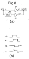
- Figure 8(a) shows the prior art driver loss compensating circuit
- Figure 8(b) shows a time chart for the same.
- the input A is supplied to an amplifier 81 which produces an output X1; at the same time, the input A is also fed into a delay circuit 83 where a delay of one cycle is introduced, and the resulting signal is inverted by an inverter amplifier 82 to obtain an inverted output X2 with a desired level.
- the outputs X1 and X2 are combined to obtain a driver output Y.
- the driver output Y has a waveform whose portion near the edge is emphasized for the time determined by one cycle.
- the prior art is the same as the present invention in that the portion near the edge is emphasized, but differs in that the output X1 is directly summed with the inverted output X, as a result of which a short circuit condition occurs and the power loss increases. Furthermore, the level of the portions other than the portion near the edge is lower than the level of the original waveform.
- the output is emphasized by increasing the driving power of the driver; as a result, the short circuiting due to the signal summing does not occur, and the edge can be further emphasized compared with the prior art. Further, even if the power for emphasizing the signal is taken into account, the total power consumption can be reduced compared with the prior art.
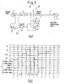
- Figure 3(a) is a diagram showing a second driver circuit
- Figure 3(b) is a time chart for the second driver circuit.
- the same constituent elements as those in Figure 2 are designated by the same reference numerals.
- the circuit configuration of the second driver circuit differs from that of the first driver circuit in that the driver unit in the second driver circuit is constructed from three drivers 31, 32, and 33 connected in parallel, and in that not only the driver 32 but also the driver 33 is controlled by the driver control signal output from the ENOR 21.
- Figure 3(b) shows the time chart for the case where the present input signal data A, the same one as that shown in the first embodiment, is applied.
- the signals A and B, the enable signal -EN, and the signal OT are the same as those shown in the first driver circuit.
- X indicates the driving power of the driver; here, since both the parallel drivers 32 and 33 are operated by the signal 0 of the enable signal -EN, the driving power is increased to three times the normal level as shown in cycles (i) to (iv).
- the driving power X of the driver is increased to three times the normal level for one cycle where a change has occurred. After that, the driving power is maintained at the normal level (unity) until a change occurs again.
- the number of drivers connected in parallel need not necessarily be limited to three.
- Figure 4 is a diagram showing an embodiment of the present invention
- Figure 5 is a time chart for the embodiment.
- This embodiment includes three parallel drivers 31, 32, and 33, as in the second driver circuit, but the control method differs.
- the third driver 33 is controlled by referring to the data two cycles back as well as to the data one cycle back. That is, in the second driver circuit, whenever a change is detected, the driving power is increased by three times; on the other hand, in the present embodiment, the third driver 33 is not driven in certain cases, thus limiting the driving power to twice the normal level.
- ENOR 22 is provided in addition to the ENOR 21, and the driver 32 is controlled by an enable signal -EN2 which is the OR of the outputs of the ENORs 21 and 22.
- the ENOR 22 takes the data A and data C at its inputs.
- the data C is a signal obtained as an output of a D-flip-flop FF 13 to which the data B is input. Since the data B is a signal obtained by delaying the data A by one cycle, it follows that the data C is a signal obtained by delaying the data A by two cycles.
- ENOR(A,B) indicates the exclusive NOR of A and B
- ENOR(A,C) indicates the exclusive NOR of A and C
- the enable signal -EN1 is ENOR(A,B)
- the enable signal -EN2 is the OR of ENOR(A,B) and ENOR(A, C).
- a B C ENOR(A,B) ENOR(A,C) -EN1 -EN2 0 0 0 1 1 1 1 0 0 1 1 0 1 0 1 0 1 0 1 0 1 0 1 (*2) 0 1 1 0 0 0 0 0 (*1) 1 0 0 0 0 0 0 (*1) 1 0 1 0 1 0 1 (*2) 1 1 0 1 0 1 0 1 1 1 1 1 1 (*1) indicates the case where both of the parallel drivers 32 and 33 are driven, thus increasing the driving power by three times to emphasize the output accordingly, while (*2) indicates the case where the parallel driver 32 is driven but the parallel driver 33 is not driven, thus limiting the driving power to twice the normal level.
- the driving power is limited to twice the normal level, as described above.
- the signals A and B, the enable signal -EN, and the signal OT are the same as those shown in the first and second driver circuit, except that the data in the subsequent cycles omitted in the first and second driver circuit are shown here.
- the driving power X of the driver will be described below for each of the cycles where the input signal changes.
- the present data OT does not match the data B one cycle back, nor does it match the data C two cycles back. This indicates the case where the signal has remained unchanged in the preceding two cycles but changes in the present cycle.
- the enable signal -EN1 is 0, but the enable signal -EN2 is 1; in this case, the parallel driver 32 is driven but the parallel driver 33 is not driven, thus limiting the driving power to twice the normal level.
- the cycles (iii) and (iv) each show the case where the present data OT does not match the data B one cycle back, but matches the data C two cycles back. That is, changes occur in succession.
- the present invention can also be viewed as providing a method of signal transmission between a driver and a receiver.
- the present invention provides a method for transmitting a transmit signal by obtaining the driver output as the transmit signal by using the driver circuit and the driver driving method described above, wherein the input data to the driver is compared with the data one cycle back, and if they are not identical, the driving power of the driver is increased to produce an output signal which is transmitted as the transmit signal ; further, the input data is further compared with the data two cycles back, and if they are identical, the factor by which to increase the driving power of the driver is reduced to produce an output signal which can then be transmitted as the transmit signal by suppressing perturbations in its waveform.
- the increase of the driving power of the driver used in the transmission method of the present invention and the reduction of the factor by which to increase the driving power, can be accomplished by operating a prescribed number of drivers selected from among three or more drivers connected in parallel.
- Figures 6 and 7 are waveform diagrams showing the results of the simulation performed of the driver circuit and the embodiment of the present invention to demonstrate the advantageous effects of the present invention.
- Each diagram was constructed by sequentially inputting 16 four-bit combinations 0000 to 1111 as input signals and by overlaying the obtained waveforms.
- the observation point indicated by Rv is the point at which the transmitted signal, having passed through the transmission line, enters the receiver.
- the length of the transmission line was set to 45 cm; in each diagram, the ordinate represents the voltage plotted with 200 mV/div. and the abscissa represents the time plotted with 1 ns/div.
- Figure 6(a) shows a reference example in which the present invention is not used.
- the circuit is fundamentally the same as that of the first embodiment shown in Figure 2(a) , except that the parallel driver 32 is omitted and the FF 12 and ENOR 21 constituting the driver control unit are removed.
- the initial amplitude of the rising and falling portions from 0 to 1 and from 1 to 0 is decreased.
- Figure 7(a) shows the simulation result of the second driver circuit; as can be seen, the initial amplitude is further improved compared with the first driver circuit.
- Figure 7(b) shows the simulation result of the embodiment; here, the same effect as achieved in the second driver circuit in improving the initial amplitude is obtained, and in addition to that, fluctuations in the waveform in the horizontal and vertical directions are reduced compared with the second driver circuit.
- (m) in the second driver circuit indicates the last 1 in a code sequence changing from 1 to 0 and to 1, and is emphasized by three times; as can be seen, it overshoots the steady-state level.
- the overshoot is eliminated as shown in (n). This is because, for the last 1 in the above code sequence, the driving power is not increased by three times but is limited to twice the normal level.
- the driver circuit and the driver driving method according to the present invention as the driving power of the driver is increased to compensate for the high frequency transmission loss of the signal, the driver circuit capable of compensating for the transmission loss can be constructed using simple circuitry.
- the driver circuit can be controlled according to the variation of the input signal to the driver circuit (for example, the variation of the input signal over time).
Landscapes
- Engineering & Computer Science (AREA)
- Computer Hardware Design (AREA)
- Physics & Mathematics (AREA)
- Computing Systems (AREA)
- General Engineering & Computer Science (AREA)
- Mathematical Physics (AREA)
- Power Engineering (AREA)
- Computer Networks & Wireless Communication (AREA)
- Signal Processing (AREA)
- Dc Digital Transmission (AREA)
- Logic Circuits (AREA)
Claims (4)
- Treiberantriebsverfahren, umfassend:Vergleichen von Eingangssignaldaten für einen Treiber (31, 32, 33) mit Daten von einem Zyklus vorher und Erhöhen der Antriebsenergie des Treibers (31, 32, 33), falls sie nicht identisch sind, undVergleichen der Eingangssignaldaten für den Treiber (31, 32, 33) mit Daten von zwei Zyklen vorher und Reduzieren des Faktors zum Erhöhen der Antriebsenergie, falls sie identisch sind.
- Treiberschaltung, umfassend:eine Treibereinheit (30), die eine Vielzahl von Treibern (31, 32, 33) hat, die parallel verbunden sind, undeine Treibersteuereinheit (20) zum Steuern der Vielzahl von Treibern (31, 32, 33), welche Treibersteuereinheit (20) umfasst:ein erstes Vergleichsmittel (20a) zum Vergleichen der Eingangssignaldaten für die Treibereinheit (30) mit Daten von einem Zyklus vorher,ein zweites Vergleichsmittel (20b) zum Vergleichen von Eingangssignaldaten für die Treibereinheit (30) mit Daten von zwei Zyklen vorher undein Freigabemittel zum Freigeben aller Treiber (31, 32, 33) der Treibereinheiten (30), falls das erste Vergleichsmittel (20a) bestimmt, dass die Eingangssignaldaten und die Daten von einem Zyklus vorher nicht identisch sind, und Sperren eines Teils der Treibereinheiten (30), falls das zweite Vergleichsmittel (20b) bestimmt, dass die Eingangssignaldaten und die Daten von zwei Zyklen vorher identisch sind.
- Treiberschaltung nach Anspruch 2, bei der die Treibereinheit (30) drei oder mehr Treiber (31, 32, 33) enthält.
- Sendeverfahren, das die Verfahrensschritte von Anspruch 1 umfasst und ferner den Schritt zum Senden eines Ausgangssignals des Treibers (31, 32, 33) an einen Empfänger umfasst.
Applications Claiming Priority (1)
| Application Number | Priority Date | Filing Date | Title |
|---|---|---|---|
| PCT/JP2002/003230 WO2003084161A1 (fr) | 2002-03-29 | 2002-03-29 | Procede d'attaque, circuit d'attaque, procede d'emission au moyen d'un circuit d'attaque et circuit de commande |
Publications (3)
| Publication Number | Publication Date |
|---|---|
| EP1492286A1 EP1492286A1 (de) | 2004-12-29 |
| EP1492286A4 EP1492286A4 (de) | 2005-03-23 |
| EP1492286B1 true EP1492286B1 (de) | 2012-02-08 |
Family
ID=28470416
Family Applications (1)
| Application Number | Title | Priority Date | Filing Date |
|---|---|---|---|
| EP02707263A Expired - Lifetime EP1492286B1 (de) | 2002-03-29 | 2002-03-29 | Treiberansteuerverfahren, treiberschaltung, übertragungsverfahren mit dem treiber und steuerschaltung |
Country Status (4)
| Country | Link |
|---|---|
| US (1) | US7149271B2 (de) |
| EP (1) | EP1492286B1 (de) |
| JP (1) | JP3976734B2 (de) |
| WO (1) | WO2003084161A1 (de) |
Families Citing this family (10)
| Publication number | Priority date | Publication date | Assignee | Title |
|---|---|---|---|---|
| JP4327504B2 (ja) | 2003-05-29 | 2009-09-09 | Necエレクトロニクス株式会社 | トランスミッタ回路、伝送回路及び駆動装置 |
| KR100755434B1 (ko) * | 2004-12-14 | 2007-09-04 | 삼성전자주식회사 | 디지털 방송수신기의 역다중화장치 및 방법 |
| KR100673897B1 (ko) * | 2005-03-02 | 2007-01-25 | 주식회사 하이닉스반도체 | 반도체 소자의 출력 드라이버 |
| US7315186B2 (en) * | 2005-06-06 | 2008-01-01 | Intel Corporation | Voltage mode driver with current mode equalization |
| JP4567086B2 (ja) | 2006-02-27 | 2010-10-20 | 富士通株式会社 | 回路基板、情報処理装置及び伝送方法 |
| KR100776740B1 (ko) * | 2006-05-08 | 2007-11-19 | 주식회사 하이닉스반도체 | 반도체 메모리의 데이터 출력장치 및 방법 |
| US7710295B2 (en) | 2006-12-22 | 2010-05-04 | Intel Corporation | Inverter based return-to-zero (RZ)+non-RZ (NRZ) signaling |
| US8766719B2 (en) | 2011-10-17 | 2014-07-01 | Mediatek Inc. | Digitally-controlled power amplifier with bandpass filtering/transient waveform control and related digitally-controlled power amplifier cell |
| US8618837B2 (en) | 2011-10-17 | 2013-12-31 | Mediatek Inc. | Multi-stage digitally-controlled power amplifier |
| US9130563B1 (en) * | 2014-05-22 | 2015-09-08 | Xilinx, Inc. | Programmable receivers and methods of implementing a programmable receiver in an integrated circuit |
Family Cites Families (14)
| Publication number | Priority date | Publication date | Assignee | Title |
|---|---|---|---|---|
| JPH06152372A (ja) * | 1992-11-04 | 1994-05-31 | Toshiba Corp | 半導体集積回路 |
| JPH09162719A (ja) * | 1995-12-08 | 1997-06-20 | Mitsubishi Electric Corp | 出力バッファ |
| JPH11239049A (ja) * | 1998-02-24 | 1999-08-31 | Matsushita Electric Ind Co Ltd | データ出力回路 |
| JP3076300B2 (ja) * | 1998-04-20 | 2000-08-14 | 日本電気アイシーマイコンシステム株式会社 | 出力バッファ回路 |
| TW440767B (en) | 1998-06-02 | 2001-06-16 | Fujitsu Ltd | Method of and apparatus for correctly transmitting signals at high speed without waveform distortion |
| JP4408470B2 (ja) | 1998-12-25 | 2010-02-03 | 富士通株式会社 | タイミング信号発生回路 |
| JP3948849B2 (ja) | 1998-12-25 | 2007-07-25 | 富士通株式会社 | レシーバ回路および信号伝送システム |
| JP3986161B2 (ja) | 1998-06-02 | 2007-10-03 | 富士通株式会社 | 信号伝送用ドライバ回路 |
| JP4030207B2 (ja) * | 1998-12-25 | 2008-01-09 | 富士通株式会社 | ドライバ回路、レシーバ回路、信号伝送システムおよび信号伝送方法 |
| JPH11355120A (ja) * | 1998-06-03 | 1999-12-24 | Mitsubishi Electric Corp | 半導体集積回路装置 |
| JP3573701B2 (ja) | 2000-09-14 | 2004-10-06 | Necエレクトロニクス株式会社 | 出力バッファ回路 |
| US6420899B1 (en) * | 2000-12-29 | 2002-07-16 | Intel Corporation | Dynamic impedance matched driver for improved slew rate and glitch termination |
| US6772250B2 (en) * | 2001-03-15 | 2004-08-03 | International Business Machines Corporation | Boundary scannable one bit precompensated CMOS driver with compensating pulse width control |
| US6518792B2 (en) * | 2001-06-11 | 2003-02-11 | Sun Microsystems, Inc. | Method and circuitry for a pre-emphasis scheme for single-ended center taped terminated high speed digital signaling |
-
2002
- 2002-03-29 JP JP2003581436A patent/JP3976734B2/ja not_active Expired - Fee Related
- 2002-03-29 WO PCT/JP2002/003230 patent/WO2003084161A1/ja not_active Ceased
- 2002-03-29 EP EP02707263A patent/EP1492286B1/de not_active Expired - Lifetime
-
2004
- 2004-09-21 US US10/944,733 patent/US7149271B2/en not_active Expired - Lifetime
Also Published As
| Publication number | Publication date |
|---|---|
| US20050035780A1 (en) | 2005-02-17 |
| EP1492286A4 (de) | 2005-03-23 |
| JPWO2003084161A1 (ja) | 2005-08-11 |
| EP1492286A1 (de) | 2004-12-29 |
| JP3976734B2 (ja) | 2007-09-19 |
| WO2003084161A1 (fr) | 2003-10-09 |
| US7149271B2 (en) | 2006-12-12 |
Similar Documents
| Publication | Publication Date | Title |
|---|---|---|
| US7164299B2 (en) | Output buffer circuit having pre-emphasis function | |
| EP1492286B1 (de) | Treiberansteuerverfahren, treiberschaltung, übertragungsverfahren mit dem treiber und steuerschaltung | |
| US6507225B2 (en) | Current mode driver with variable equalization | |
| EP0763917A2 (de) | Leitungstreiber mit Impulsformer | |
| US20060267651A1 (en) | Devices and methods for controlling a slew rate of a signal line | |
| EP1911232B1 (de) | Vorverzerrungs- und Rückentzerrungsschaltung. | |
| US10848352B1 (en) | Time based feed forward equalization (TFFE) for high-speed DDR transmitter | |
| WO2019001369A1 (zh) | 一种串行解串链路发射机的驱动器 | |
| KR102421896B1 (ko) | Ffe 및 xtc가 융합된 트랜스미터 및 전송방법 | |
| US7373114B2 (en) | Signal transmission circuit, signal output circuit and termination method of signal transmission circuit | |
| JPH11112325A (ja) | 出力バッファ回路 | |
| US7126395B2 (en) | Dynamic slew rate controlling method and device for reducing variance in simultaneous switching output | |
| US7155006B2 (en) | Method and apparatus for outbound wave subtraction using a variable offset amplifier | |
| US6803820B1 (en) | Apparatus and method for reducing common-mode current in differential link | |
| US12119963B2 (en) | Feed forward equalizer and system including the same | |
| US7898293B2 (en) | Circuit board, information processing apparatus, and transmission method | |
| US7378877B2 (en) | Output buffer circuit | |
| US8698537B1 (en) | Method and apparatus for reducing jitter in a transmitter | |
| JP4320291B2 (ja) | 送受信回路 | |
| JPH08237105A (ja) | バスドライバ | |
| CN101420510A (zh) | 应用于多媒体接口的时钟的产生装置及其相关方法 | |
| JP2001127614A (ja) | 半導体集積回路及びそのインピーダンス制御方法 | |
| CN121257448B (zh) | Ddr输出驱动器电路和ddr芯片 | |
| US6487673B1 (en) | Clock circuit and a computer system having said clock circuit | |
| US20060044894A1 (en) | Enhanced timing margin memory interface |
Legal Events
| Date | Code | Title | Description |
|---|---|---|---|
| PUAI | Public reference made under article 153(3) epc to a published international application that has entered the european phase |
Free format text: ORIGINAL CODE: 0009012 |
|
| 17P | Request for examination filed |
Effective date: 20041025 |
|
| AK | Designated contracting states |
Kind code of ref document: A1 Designated state(s): AT BE CH CY DE DK ES FI FR GB GR IE IT LI LU MC NL PT SE TR |
|
| A4 | Supplementary search report drawn up and despatched |
Effective date: 20050209 |
|
| RIC1 | Information provided on ipc code assigned before grant |
Ipc: 7H 04L 25/02 A Ipc: 7H 03K 19/017 B Ipc: 7G 06F 3/00 B Ipc: 7H 03K 19/00 B |
|
| 17Q | First examination report despatched |
Effective date: 20080801 |
|
| GRAP | Despatch of communication of intention to grant a patent |
Free format text: ORIGINAL CODE: EPIDOSNIGR1 |
|
| RIC1 | Information provided on ipc code assigned before grant |
Ipc: H04L 25/02 20060101AFI20110810BHEP Ipc: H03K 19/00 20060101ALI20110810BHEP Ipc: H03K 19/0175 20060101ALI20110810BHEP Ipc: G06F 3/00 20060101ALI20110810BHEP Ipc: H03K 19/017 20060101ALI20110810BHEP |
|
| GRAS | Grant fee paid |
Free format text: ORIGINAL CODE: EPIDOSNIGR3 |
|
| GRAA | (expected) grant |
Free format text: ORIGINAL CODE: 0009210 |
|
| AK | Designated contracting states |
Kind code of ref document: B1 Designated state(s): DE GB |
|
| REG | Reference to a national code |
Ref country code: GB Ref legal event code: FG4D |
|
| REG | Reference to a national code |
Ref country code: DE Ref legal event code: R096 Ref document number: 60242172 Country of ref document: DE Effective date: 20120329 |
|
| PLBE | No opposition filed within time limit |
Free format text: ORIGINAL CODE: 0009261 |
|
| STAA | Information on the status of an ep patent application or granted ep patent |
Free format text: STATUS: NO OPPOSITION FILED WITHIN TIME LIMIT |
|
| 26N | No opposition filed |
Effective date: 20121109 |
|
| REG | Reference to a national code |
Ref country code: DE Ref legal event code: R097 Ref document number: 60242172 Country of ref document: DE Effective date: 20121109 |
|
| PGFP | Annual fee paid to national office [announced via postgrant information from national office to epo] |
Ref country code: DE Payment date: 20200317 Year of fee payment: 19 Ref country code: GB Payment date: 20200318 Year of fee payment: 19 |
|
| REG | Reference to a national code |
Ref country code: DE Ref legal event code: R119 Ref document number: 60242172 Country of ref document: DE |
|
| GBPC | Gb: european patent ceased through non-payment of renewal fee |
Effective date: 20210329 |
|
| PG25 | Lapsed in a contracting state [announced via postgrant information from national office to epo] |
Ref country code: DE Free format text: LAPSE BECAUSE OF NON-PAYMENT OF DUE FEES Effective date: 20211001 Ref country code: GB Free format text: LAPSE BECAUSE OF NON-PAYMENT OF DUE FEES Effective date: 20210329 |