EP1492996B1 - Arrangement d'un systeme de mesure - Google Patents
Arrangement d'un systeme de mesure Download PDFInfo
- Publication number
- EP1492996B1 EP1492996B1 EP03708805.1A EP03708805A EP1492996B1 EP 1492996 B1 EP1492996 B1 EP 1492996B1 EP 03708805 A EP03708805 A EP 03708805A EP 1492996 B1 EP1492996 B1 EP 1492996B1
- Authority
- EP
- European Patent Office
- Prior art keywords
- area
- sensor
- resolution
- output register
- image
- Prior art date
- Legal status (The legal status is an assumption and is not a legal conclusion. Google has not performed a legal analysis and makes no representation as to the accuracy of the status listed.)
- Expired - Lifetime
Links
Images



Classifications
-
- G—PHYSICS
- G01—MEASURING; TESTING
- G01B—MEASURING LENGTH, THICKNESS OR SIMILAR LINEAR DIMENSIONS; MEASURING ANGLES; MEASURING AREAS; MEASURING IRREGULARITIES OF SURFACES OR CONTOURS
- G01B11/00—Measuring arrangements characterised by the use of optical techniques
- G01B11/24—Measuring arrangements characterised by the use of optical techniques for measuring contours or curvatures
-
- G—PHYSICS
- G06—COMPUTING OR CALCULATING; COUNTING
- G06T—IMAGE DATA PROCESSING OR GENERATION, IN GENERAL
- G06T1/00—General purpose image data processing
- G06T1/0007—Image acquisition
-
- G—PHYSICS
- G01—MEASURING; TESTING
- G01B—MEASURING LENGTH, THICKNESS OR SIMILAR LINEAR DIMENSIONS; MEASURING ANGLES; MEASURING AREAS; MEASURING IRREGULARITIES OF SURFACES OR CONTOURS
- G01B11/00—Measuring arrangements characterised by the use of optical techniques
- G01B11/02—Measuring arrangements characterised by the use of optical techniques for measuring length, width or thickness
- G01B11/04—Measuring arrangements characterised by the use of optical techniques for measuring length, width or thickness specially adapted for measuring length or width of objects while moving
-
- G—PHYSICS
- G06—COMPUTING OR CALCULATING; COUNTING
- G06T—IMAGE DATA PROCESSING OR GENERATION, IN GENERAL
- G06T7/00—Image analysis
- G06T7/0002—Inspection of images, e.g. flaw detection
- G06T7/0004—Industrial image inspection
Definitions
- the present invention relates in general to a sensor and a system for imaging characteristics of an object and relates in particular to a sensor and system for imaging multiple characteristics of an object with different degrees of resolution.
- NxM matrix array
- photodiodes which absorb electromagnetic radiation and convert this into electrical signals.
- 3D three-dimensional
- 2D image characteristics such as cracks, structural orientation, position and identity are imaged, for example, through marks, bar code or matrix code.
- Intensity information in the 2D image is usually imaged in grey scale, but imaging the 2D image in colour, that is to say registering R (red), G (green) and B (blue) components, for example, by means of filters or light wavelengths is also common.
- a matrix array picture processor (MAPP sensor) is used for imaging different characteristics of the same object using the same sensor, so-called multisensing, by using a part of the sensor for laser profiling (3D measurement) and individual sensor rows for reading out intensity Information (2D measurement).
- MAPP sensor matrix array picture processor
- An advantage in using one sensor to image multiple characteristics is that the cost and complexity of the system are less than when using one sensor for the 3D measurement and another sensor for the 2D measurement, for example.
- imaging sensors which have different degrees of resolution are shown in Allreza Molni "Vision chips", Kluwer Academic Publishers, page 143-146, 2000 , in which image sensors are constructed as an electronic eye, that is to say they have a high resolution in the centre and a low resolution at the periphery.
- the pixel geometry in these "eyes” is linear-polar or log-polar. If the "eye” sees something interesting at its periphery with a low resolution, the system can control the sensor so that it directs its high-resolution centre part to the area In order to read the details. This type of sensor is very well suited for robot applications.
- An example of such an electronic eye is also shown in US 5,166,511 .
- U.S. Patent No. 6,122,046 discloses an optical inspection system for inspecting a substrate and includes a light detector, a light source, a deflection system, an objective lens and an optical system.
- the light source produces an illuminating beam directed along a path to the substrate.
- the deflection system scans the illuminating beam on a scan line of the substrate.
- the objective lens focuses the illuminating beam on the substrate and collects light reflected therefrom.
- the collected beam is angularly wider than the illuminating beam.
- the optical system directs the collected light beam along a path at least partially different than the path of the illuminating beam and focuses the collected beam on the light detector.
- the system additionally includes at least one dark field detector for collecting light deflected from the substrate.
- WO 00/42381 A1 discloses a method for contactless inspection of objects on a substrate, by means of an inspection device during relative motion between the substrate and the inspection device.
- the method comprises the steps of: generating a first image comprising object height information by illuminating at least a portion of the substrate comprising one or more objects by means of first radiation means and imaging at least one of the one or more objects illuminated by the first radiation means onto a two-dimensional matrix sensor means having a portionwise addressable matrix of pixel elements; generating a second image comprising object area information by illuminating at least a portion of the substrate comprising one or more objects by means of second radiation means and imaging at least one of the one or more objects illuminated by the second radiation means onto the sensor means; extracting the object height information, by means of the sensor means, from the first image; and extracting the object area information, by means of the sensor means, from the second image.
- European Patent EP 0 840 880 discloses a scanning apparatus and method for generating computer models of three dimensional objects comprising means for scanning the object to capture data from a plurality of points on the surface of the object so that the scanning means may capture data from two or more points simultaneously; sensing the position of the scanning means; generating intermediate data structures from the data; combining intermediate data structures to provide the model; display; and for manually operating the scanning apparatus.
- the signal generated is structured light in the form of stripe or area from illumination sources such as a laser diode or bulbs which enable data for the position and colour of the surface to be determined.
- the object is preferably widely illuminated with a reflecting means for each bulb to provide a more uniform light intensity and a diffusing means and/or polarising means.
- the position sensing means may be a multiply jointed arm or a remote position sensing means.
- the object may be on a turntable and may be viewed in real time as rendered polygons on a monitor as the object is scanned.
- U.S. Patent No. 5,796,095 discloses an optical apparatus including area sensors which are made to differ in picture element pitch between the central portions and the marginal portions thereof (the marginal portions are made to have a coarse picture element pitch since it is not very meaningful even if the picture element pitch is made fine because the performance of an optical system is limited, and the central portions are made to have a dense picture element pitch) and the changeover of the respective picture elements is electronically effected by reading-out means so that two kinds of object field information (detailed information and coarse information) may be obtained from the area sensors.
- European Patent EP 1 096 785 discloses a photosensor array having at least one row of photosensors with a first sensor size, and at least one row of photosensors with a second sensor size, with the two sizes being different.
- each sensor in a row of sensors for white light (206, has a smaller area than the sensors in other rows.
- the native input sampling rate for luminance is greater than the native input sampling rate for color information.
- the rows with relatively small sensor areas are used for high native input sampling rates, and the rows with relatively large sensor areas are used for high color accuracy.
- US 6,320,618 Another example of an imaging sensor which has different degrees of resolution is shown In US 6,320,618 , in which an array matrix-type sensor has been provided with at least one area having a higher resolution than the rest of the sensor.
- the sensor is placed In a camera, which is mounted on a vehicle as a part of an automatic navigation system, which controls functions of the vehicle, for example braking if some obstacle appears in front of the car or steering along the white line at the edge of the road.
- the sensor is arranged to pick up remote information with a high resolution and information in proximity to the vehicle with a low resolution.
- An object of the present invention is to provide a sensor and a system which image the characteristics of an object with different degrees of resolution. This has been achieved by a system having the characteristics specified in the characterising part of claim 1.
- a system according to the invention furthermore requires fewer system components such as cameras, lenses etc.
- the senor comprises two integral areas with pixels which are arranged substantially parallel, side by side In a transverse direction.
- the two pixel areas/units share read-out logic, which means that they have the same output register.
- the two pixel areas/units are each read out on different output registers, which means that it is possible to read out the information contained In the two areas/units simultaneously.
- One advantage to this is that it obtains greater freedom with regard to exposure times.
- Another advantage is that it obtains greater freedom with regard to degrees of resolution in both the transverse direction and the longitudinal direction.
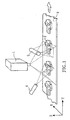
- Figure 1 shows a system for reading in characteristics of an object.
- the system comprises a camera 1, which may be an MAPP camera, a CCD camera, a CMOS camera or any other camera suitable for imaging characteristics of an object.
- the system further comprises an object 2, the characteristic-dependent parameters of which are to be measured by the system, placed on a base 3 together with two light sources 4 and 5 arranged to illuminate the object 2.
- the light sources 4, 5 generate, for example, substantially point light, substantially linear light or light composed of multiple, substantially point or linear segments and may be of any type suited to the application, for example lasers, LED's, ordinary light (light bulb) etc, but these are familiar to the person skilled in the art and will not be further described here.
- the camera 1 comprises, among other things, a sensor 10, which is shown in Figures 2 to 5 and is described in more detail below, light-gathering optics and control logic (not shown).
- the rays reflected from the object 2 are picked up by the sensor 10 and are converted there Into electrical charges, which are in turn converted into analog or digital electrical signals.
- these signals are then transferred via an output register (shown in Figures 6 and 7 ) to an image/signal-processing unit (not shown) to be analysed and processed.
- the object 2 which as stated above, has been placed on the base 3, which in a preferred embodiment moves relative to the measuring system indicated by an arrow in the figure.
- the relationship may naturally be reversed, that is to say the object 3 is fixed and the measuring system moves over the object 2 when measuring.
- the base 3 may be a conveyor belt, for example, or alternatively there is no base and the object itself moves, if the said object is paper, for example, in a continuous web in a paper-making machine.
- one or more of the light sources is located below the base 3 and shines through the object 2, which means that the sensor 10 picks up transmitted rays which have passed through the object 2, and not reflected rays.
- the direction of movement is indicated by an arrow.
- This direction will be referred to in this document as the longitudinal direction, that is to say Y in the system of coordinates drawn into the figure.
- the transverse direction (X in the system of coordinates) lies perpendicular to the longitudinal direction.
- the longitudinal resolution depends on how frequently the object 2 is read off (sampled).
- the present invention is primarily concerned with the transverse resolution, which largely depends on the number of pixels which the sensor 10 has in a row.
- the first area 11 is used for 3D measurement by triangulation, that is to say imaged geometric characteristics of the object 2 such as width, height, volume etc.
- the intensity image is reduced from k rows, k>1, to the position values that correspond to where the light strikes the sensor in each column. The result is a profile with three-dimensional information for each sample of k rows.
- the second area 12 is used For 2D measurement (intensity information), that is to say In imaged characteristics of the object 2 such as cracks, structural orientation, position etc. If N' ⁇ 2, there is a possibility of applying colour filters (for example, RGB) to the individual pixels and In this way obtaining a colour read-out of 2D data.
- colour filters for example, RGB
- Figure 2 shows a 3D profile of the object 2 in the first area 11 and a grey scale/colour Image of the object 2 in the second area 12.
- the object 2 is scanned profile by profile as the object 2 passes the measuring system and the result is accordingly a three-dimensional and a two-dimensional imaging of the object 2.
- MAPP sensor In the preferred embodiment an MAPP sensor is used, but the person skilled In the art will appreciate that the invention may be applied to other types of sensors, such as CCD sensors or CMOS sensors, for example.
- Figure 3 shows a first embodiment of the sensor according to the invention.
- every other row in the second high-resolution area 12 is offset half a pixel width in relation to the rows immediately below and above.
- the invention is not limited to the embodiments shown in Figures 3 and 4 .
- the pixels may be half the width of those in the first area 11, or also at the same time twice as high etc.
- Other variants of the embodiment according to Figure 4 may involve the pixels being offset by a third or a quarter of the pixel width.
- US 4,204,230 which shows offset pixel rows for increasing the resolution of an imaging sensor.
- the first area 11 and the second area 12 lie substantially parallel side by side in direct contact In a longitudinal direction, that it to say the sensor is manufactured as an integral unit.
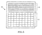
- Figure 5 shows a sensor - not claimed - in which the first area 11 and the second area 12 are two separate units lying substantially parallel side by side in the transverse direction, but not In direct contact.
- the second high-resolution area 12 is located longitudinally In front of the first area 11 (illustrated at the top of the figures), but naturally it may equally well be located longitudinally behind the first area 11 (illustrated at the bottom of the figures).
- An alternative to designing the pixels offset in relation to one another is to cover the pixels with masks, which are arranged in such a way that illumination of parts of pixels is blocked and an offset sampling pattern is thereby obtained.
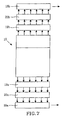
- a sensor row is read out to an output register, which is M pixels long, shown in Figures 6 and 7 .
- This output register 15, 18a, 18b is either exchanged as raw data or it is coupled to a row-parallel A/D converter and/or signal/image processing unit.
- w read-outs In order to read out a Y-wide row, w read-outs must be performed successively. If the output register 15, 18a, 18b has space for b rows, these can be read out/processed together.
- the read-out can therefore be both analog and digital, but in the preferred embodiment of the present invention (shown in Figure 6 ), measured data is read out via an A/D converter 16 and a processor 17 to a digital output register 15, before being relayed to an image-processing unit (not shown).
- the processor 17 can be programmed to perform many functions, among other things extracting the three-dimensional profile from the intensity image, that is to say each column calculates the position of the lightest point and these values can then be seen as an intensity profile in which the intensity corresponds to distance.
- Other functions performed by the processor 17 are edge detection, noise reduction etc.
- the two sensor areas 11, 12 do not share the read-out logic, that is to say they have different output registers 18a and 18b, which means that other effects are obtained.
- Information from the two areas 11, 12 can be read out independently of one another with greater freedom of exposure times and degrees of resolution both in the transverse and in the longitudinal direction.
- measured data are read out via A/D converters 19a, 19b and processors 20a, 20b to digital output registers 18a, 18b.
- colour filters or coloured light sources (not shown) on the second area 12 of the sensor 10, which means that both grey scale and colour images can be read out with the higher resolution.
- colour filters or coloured light sources which colour filters or coloured light sources are used and how these are placed will be known to the person skilled In the art and will not be described in detail here, but the possible use of Bayer patterns or a filter for each row may be mentioned by way of example.
- RGB components are commonly chosen, but other colours such as CMY (cyan magenta yellow) may also be used.
- CMY cyan magenta yellow
- each colour might have its own output register, which gives a faster read-out of each colour profile.
- Crosstalk means that light from one measurement interferes with another sensor area, that is to say light from the 3D measurement interferes with the 2D measurement and/or vice-versa.
- light from the 3D measurement interferes with the 2D measurement and/or vice-versa.
- optical filters differing according to wavelength, which block the light or allow it to pass through to the respective sensor area.
- time delay integration is used on the high-resolution second area 12.
- TDI means that the charge is moved from one row to another as the object 2 is moved with the base 3, thereby achieving an X-times greater light sensitivity with X TDI stages.
Landscapes
- Physics & Mathematics (AREA)
- General Physics & Mathematics (AREA)
- Engineering & Computer Science (AREA)
- Theoretical Computer Science (AREA)
- Quality & Reliability (AREA)
- Computer Vision & Pattern Recognition (AREA)
- Length Measuring Devices By Optical Means (AREA)
- Solid State Image Pick-Up Elements (AREA)
- Transforming Light Signals Into Electric Signals (AREA)
- Image Input (AREA)
- Investigating Or Analysing Materials By Optical Means (AREA)
Claims (11)
- Système destiné à mesurer des paramètres dépendant de caractéristiques d'un objet (2) comprenant au moins une source de lumière (4, 5), qui émet de la lumière vers l'objet (2), dont les caractéristiques sont à imager, ledit système comprenant un moyen (3) permettant de déplacer ledit objet dans une direction longitudinale par rapport audit système, ledit système comprenant en outre un capteur (10) qui comprend lui-même au moins une première aire (11) et une seconde aire (12) d'éléments de pixel agencés pour absorber le rayonnement électromagnétique provenant dudit objet (2) et pour convertir le rayonnement absorbé en charges électriques, qui sont elles-mêmes converties en signaux électriques, dans lequel la première aire (11) et la seconde aire (12) sont agencées parallèlement côte à côte en contact direct dans ladite direction longitudinale comme une unité d'un seul tenant, ladite première aire (11) ayant un premier degré de résolution transversale (M) et étant adaptée pour des mesures en 3D dudit objet (2), et ladite seconde aire (12) ayant un second degré de résolution transversale (M') et étant adaptée pour des mesures en 2D dudit objet (2), ledit système comprenant en outre une unité de traitement d'image/de signal destinée à analyser et traiter lesdits signaux provenant de la première aire par triangulation en utilisant ladite au moins une source de lumière (4, 5) pour fournir des caractéristiques géométriques tridimensionnelles de l'objet (2), et lesdits signaux provenant de la seconde aire pour fournir des caractéristiques imagées bidimensionnelles dudit objet (2), caractérisé en ce que ledit second degré de résolution transversale (M' = M x b) est supérieur (b > 1) audit premier degré de résolution transversale (M).
- Système selon la revendication 1, caractérisé en ce qu'au moins l'une des deux aires (11, 12) est dotée dans son intégralité ou en partie de filtres colorés pour imager l'objet (2) en couleur.
- Système selon la revendication 1 ou 2, dans lequel la première aire (11) est conçue comme une matrice ayant N lignes et M colonnes, la seconde aire (12) est conçue comme une matrice ayant N' lignes et M' colonnes et M' est b multiplié par M colonnes, où b est un entier supérieur à un.
- Système selon la revendication 3, dans lequel une intégration à retard de temps (TDI) est utilisée sur la seconde aire (12).
- Système selon la revendication 1, caractérisé en ce qu'au moins une des aires (11, 12) est dotée de filtres pour différentes longueurs d'onde pour minimiser la diaphonie.
- Système selon l'une quelconque des revendications précédentes, dans lequel le système comprend également un registre de sortie (15) agencé pour lire les charges reçues dans le capteur (10).
- Système selon l'une quelconque des revendications 1 à 6, dans lequel le système comprend également au moins deux registres de sortie (18a, 18b) agencés pour lire les charges reçues dans le capteur (10).
- Système selon la revendication 7, dans lequel la première aire (11) et la seconde aire (12) du capteur (10) sont chacune lues sur leur propre registre de sortie (18a, 18b).
- Système selon la revendication 7, dans lequel si la seconde aire (12) du capteur est dotée de filtres colorés, chaque couleur captée a son propre registre de sortie.
- Système selon la revendication 6 ou 7, dans lequel le système comprend en outre un convertisseur A/N (16) agencé pour convertir les charges électriques d'un format analogique à numérique et le registre de sortie (15, 18a, 18b) est un registre de sortie numérique.
- Système selon l'une quelconque des revendications précédentes, dans lequel le système comprend également une unité de traitement d'image/de signal agencée pour analyser les charges électriques.
Applications Claiming Priority (3)
| Application Number | Priority Date | Filing Date | Title |
|---|---|---|---|
| SE0201044A SE523681C2 (sv) | 2002-04-05 | 2002-04-05 | System och sensor för avbildning av egenskaper hos ett objekt |
| SE0201044 | 2002-04-05 | ||
| PCT/SE2003/000461 WO2003087713A1 (fr) | 2002-04-05 | 2003-03-19 | Dispositif et systeme de mesure des caracteristiques d'un objet |
Publications (2)
| Publication Number | Publication Date |
|---|---|
| EP1492996A1 EP1492996A1 (fr) | 2005-01-05 |
| EP1492996B1 true EP1492996B1 (fr) | 2014-03-12 |
Family
ID=20287507
Family Applications (1)
| Application Number | Title | Priority Date | Filing Date |
|---|---|---|---|
| EP03708805.1A Expired - Lifetime EP1492996B1 (fr) | 2002-04-05 | 2003-03-19 | Arrangement d'un systeme de mesure |
Country Status (8)
| Country | Link |
|---|---|
| US (1) | US20050151863A1 (fr) |
| EP (1) | EP1492996B1 (fr) |
| JP (1) | JP2005522920A (fr) |
| CN (1) | CN1293361C (fr) |
| AU (1) | AU2003212775A1 (fr) |
| CA (1) | CA2477955C (fr) |
| SE (1) | SE523681C2 (fr) |
| WO (1) | WO2003087713A1 (fr) |
Families Citing this family (17)
| Publication number | Priority date | Publication date | Assignee | Title |
|---|---|---|---|---|
| EP1758783B1 (fr) * | 2004-05-25 | 2008-04-16 | VDO Automotive AG | Unite de surveillance associee a un systeme d'assistance pour un vehicule |
| EP3920079B1 (fr) * | 2005-03-11 | 2023-06-28 | Hand Held Products, Inc. | Lecteur optique pouvant prendre des clichés numériques avec ensemble de capteurs pour image monochrome et image couleur |
| US7568628B2 (en) | 2005-03-11 | 2009-08-04 | Hand Held Products, Inc. | Bar code reading device with global electronic shutter control |
| US7780089B2 (en) | 2005-06-03 | 2010-08-24 | Hand Held Products, Inc. | Digital picture taking optical reader having hybrid monochrome and color image sensor array |
| US7611060B2 (en) | 2005-03-11 | 2009-11-03 | Hand Held Products, Inc. | System and method to automatically focus an image reader |
| US7770799B2 (en) | 2005-06-03 | 2010-08-10 | Hand Held Products, Inc. | Optical reader having reduced specular reflection read failures |
| US7528943B2 (en) * | 2005-12-27 | 2009-05-05 | Kla-Tencor Technologies Corporation | Method and apparatus for simultaneous high-speed acquisition of multiple images |
| JP5538223B2 (ja) * | 2008-07-18 | 2014-07-02 | 瀬戸製材株式会社 | 木材の管理システム |
| FI20106053A0 (fi) * | 2010-10-13 | 2010-10-13 | Metso Automation Oy | Järjestelmä rainan tarkkailemiseksi ja vastaava menetelmä rainan tarkkailemiseksi |
| CN102175172B (zh) * | 2010-12-30 | 2012-07-04 | 南京理工大学 | 一种基于图像识别的机动车辆外形尺寸检测系统 |
| US10368053B2 (en) * | 2012-11-14 | 2019-07-30 | Qualcomm Incorporated | Structured light active depth sensing systems combining multiple images to compensate for differences in reflectivity and/or absorption |
| DE102014213289A1 (de) * | 2014-07-09 | 2016-01-14 | Robert Bosch Gmbh | Verfahren und Vorrichtung zur dreidimensionalen optischen Erfassung eines Objekts |
| JP2017098830A (ja) * | 2015-11-26 | 2017-06-01 | キヤノン株式会社 | 放射線撮像装置、放射線撮像システム及び放射線撮像装置の製造方法 |
| DE102016220757A1 (de) * | 2016-10-21 | 2018-04-26 | Texmag Gmbh Vertriebsgesellschaft | Verfahren und Vorrichtung zur Materialbahnbeobachtung und Materialbahninspektion |
| US11507097B2 (en) | 2018-02-05 | 2022-11-22 | Pixart Imaging Inc. | Control apparatus for auto clean machine and auto clean machine control method |
| JP7489169B2 (ja) * | 2018-11-30 | 2024-05-23 | セイコーエプソン株式会社 | 画像読取装置 |
| CN112019777B (zh) * | 2020-09-16 | 2021-10-26 | 南京大学 | 基于时间延迟积分(tdi)的图像传感器及其成像方法 |
Citations (4)
| Publication number | Priority date | Publication date | Assignee | Title |
|---|---|---|---|---|
| US5796095A (en) * | 1995-06-19 | 1998-08-18 | Canon Kabushiki Kaisha | Optical apparatus having an area sensor with a coarse picture element pitch and fine picture element pitch |
| US6122046A (en) * | 1998-10-02 | 2000-09-19 | Applied Materials, Inc. | Dual resolution combined laser spot scanning and area imaging inspection |
| EP1096785A2 (fr) * | 1999-10-29 | 2001-05-02 | Hewlett-Packard Company, A Delaware Corporation | Photocapteur avec multiples zones de capteurs différents. |
| EP0840880B1 (fr) * | 1995-07-26 | 2002-03-13 | Stephen James Crampton | Appareil de balayage et procede |
Family Cites Families (11)
| Publication number | Priority date | Publication date | Assignee | Title |
|---|---|---|---|---|
| US4204230A (en) | 1978-10-25 | 1980-05-20 | Xerox Corporation | High resolution input scanner using a two dimensional detector array |
| NL8901156A (nl) * | 1989-05-08 | 1990-12-03 | Imec Inter Uni Micro Electr | Stralingsgevoelig orgaan of sensor in retina-achtige configuratie. |
| IL99823A0 (en) * | 1990-11-16 | 1992-08-18 | Orbot Instr Ltd | Optical inspection method and apparatus |
| US5355309A (en) * | 1992-12-30 | 1994-10-11 | General Electric Company | Cone beam spotlight imaging using multi-resolution area detector |
| DE69528946T2 (de) * | 1994-09-22 | 2003-10-02 | Sanyo Electric Co., Ltd. | Verfahren zum Umsetzen von zweidimensionalen Bildern in dreidimensionale Bilder |
| JPH09247545A (ja) * | 1996-03-11 | 1997-09-19 | Matsushita Electric Ind Co Ltd | スキャナ型電子カメラ |
| JP3832902B2 (ja) | 1996-08-30 | 2006-10-11 | 本田技研工業株式会社 | 半導体イメージセンサ |
| SE514859C2 (sv) * | 1999-01-18 | 2001-05-07 | Mydata Automation Ab | Förfarande och anordning för undersökning av objekt på ett substrat genom att ta bilder av substratet och analysera dessa |
| US7034272B1 (en) * | 1999-10-05 | 2006-04-25 | Electro Scientific Industries, Inc. | Method and apparatus for evaluating integrated circuit packages having three dimensional features |
| US6750899B1 (en) * | 2000-01-07 | 2004-06-15 | Cyberoptics Corporation | Solder paste inspection system |
| US6683704B1 (en) * | 2000-05-12 | 2004-01-27 | Hewlett-Packard Development Company, L.P. | Apparatus for determining the best image from a dual resolution photo sensor |
-
2002
- 2002-04-05 SE SE0201044A patent/SE523681C2/sv not_active IP Right Cessation
-
2003
- 2003-03-19 JP JP2003584615A patent/JP2005522920A/ja active Pending
- 2003-03-19 US US10/510,208 patent/US20050151863A1/en not_active Abandoned
- 2003-03-19 AU AU2003212775A patent/AU2003212775A1/en not_active Abandoned
- 2003-03-19 EP EP03708805.1A patent/EP1492996B1/fr not_active Expired - Lifetime
- 2003-03-19 WO PCT/SE2003/000461 patent/WO2003087713A1/fr not_active Ceased
- 2003-03-19 CA CA2477955A patent/CA2477955C/fr not_active Expired - Lifetime
- 2003-03-19 CN CNB038068052A patent/CN1293361C/zh not_active Expired - Lifetime
Patent Citations (4)
| Publication number | Priority date | Publication date | Assignee | Title |
|---|---|---|---|---|
| US5796095A (en) * | 1995-06-19 | 1998-08-18 | Canon Kabushiki Kaisha | Optical apparatus having an area sensor with a coarse picture element pitch and fine picture element pitch |
| EP0840880B1 (fr) * | 1995-07-26 | 2002-03-13 | Stephen James Crampton | Appareil de balayage et procede |
| US6122046A (en) * | 1998-10-02 | 2000-09-19 | Applied Materials, Inc. | Dual resolution combined laser spot scanning and area imaging inspection |
| EP1096785A2 (fr) * | 1999-10-29 | 2001-05-02 | Hewlett-Packard Company, A Delaware Corporation | Photocapteur avec multiples zones de capteurs différents. |
Also Published As
| Publication number | Publication date |
|---|---|
| CA2477955A1 (fr) | 2003-10-23 |
| CN1643337A (zh) | 2005-07-20 |
| SE523681C2 (sv) | 2004-05-11 |
| CN1293361C (zh) | 2007-01-03 |
| EP1492996A1 (fr) | 2005-01-05 |
| US20050151863A1 (en) | 2005-07-14 |
| SE0201044L (sv) | 2003-10-06 |
| CA2477955C (fr) | 2014-05-27 |
| AU2003212775A1 (en) | 2003-10-27 |
| WO2003087713A1 (fr) | 2003-10-23 |
| JP2005522920A (ja) | 2005-07-28 |
| SE0201044D0 (sv) | 2002-04-05 |
Similar Documents
| Publication | Publication Date | Title |
|---|---|---|
| EP1492996B1 (fr) | Arrangement d'un systeme de mesure | |
| US7573569B2 (en) | System for 2-D and 3-D vision inspection | |
| JP7026309B2 (ja) | 光学式外観検査装置、及びこれを用いた光学式外観検査システム | |
| US6369401B1 (en) | Three-dimensional optical volume measurement for objects to be categorized | |
| JP4803568B2 (ja) | 半導体集積回路の検査装置および検査方法 | |
| KR100602765B1 (ko) | 대상체를 검사하기 위한 방법 및 장치 | |
| JP2954708B2 (ja) | 多焦点結像システム | |
| CA2017518A1 (fr) | Imagerie a determination du spectre de couleurs | |
| EP1359534A1 (fr) | Méthode et système pour enregistrer un objet ou une forme | |
| JP2005504305A (ja) | 三次元走査カメラ | |
| US20080007722A1 (en) | Vehicle wheel alignment system scanned beam imaging sensor | |
| CA2375741A1 (fr) | Procede/systeme de mesure de caracteristiques d'un objet avec coordination d'imagerie 2d et 3d | |
| WO1997033139A1 (fr) | Imagerie tridimensionnelle en couleurs | |
| JPH07502408A (ja) | 植物の光学的品質管理および/または分類方法および装置 | |
| US7315383B1 (en) | Scanning 3D measurement technique using structured lighting and high-speed CMOS imager | |
| US5701173A (en) | Method and apparatus for reducing the unwanted effects of noise present in a three dimensional color imaging system | |
| CN114390152B (zh) | 检测微小凹凸的接触式图像传感器及应用 | |
| EP4220075B1 (fr) | Procédé et dispositifs pour obtenir et associer des données d'images 2d avec des données d'images 3d à partir d'une triangulation optique | |
| US20190349569A1 (en) | High-sensitivity low-power camera system for 3d structured light application | |
| KR100651791B1 (ko) | 부품 검사 장치 및, 방법 | |
| JP2004260250A (ja) | 撮像素子 | |
| JP2025033134A (ja) | 計測装置 | |
| JPH11104938A (ja) | 板金加工における画像処理方法およびその装置 | |
| CA2473296A1 (fr) | Lecture optique simultanee de niveaux de gris dans trois dimensions |
Legal Events
| Date | Code | Title | Description |
|---|---|---|---|
| PUAI | Public reference made under article 153(3) epc to a published international application that has entered the european phase |
Free format text: ORIGINAL CODE: 0009012 |
|
| 17P | Request for examination filed |
Effective date: 20040910 |
|
| AK | Designated contracting states |
Kind code of ref document: A1 Designated state(s): AT BE BG CH CY CZ DE DK EE ES FI FR GB GR HU IE IT LI LU MC NL PT RO SE SI SK TR |
|
| AX | Request for extension of the european patent |
Extension state: AL LT LV MK |
|
| RAP1 | Party data changed (applicant data changed or rights of an application transferred) |
Owner name: SICK IVP AB |
|
| 17Q | First examination report despatched |
Effective date: 20100622 |
|
| REG | Reference to a national code |
Ref country code: DE Ref legal event code: R079 Ref document number: 60345835 Country of ref document: DE Free format text: PREVIOUS MAIN CLASS: G01B0011040000 Ipc: H01L0027140000 |
|
| GRAP | Despatch of communication of intention to grant a patent |
Free format text: ORIGINAL CODE: EPIDOSNIGR1 |
|
| RIC1 | Information provided on ipc code assigned before grant |
Ipc: G01B 11/24 20060101ALI20130426BHEP Ipc: G01B 11/04 20060101ALI20130426BHEP Ipc: H04N 5/335 20110101ALI20130426BHEP Ipc: H01L 27/14 20060101AFI20130426BHEP Ipc: H04N 13/00 20060101ALI20130426BHEP |
|
| INTG | Intention to grant announced |
Effective date: 20130521 |
|
| GRAP | Despatch of communication of intention to grant a patent |
Free format text: ORIGINAL CODE: EPIDOSNIGR1 |
|
| INTG | Intention to grant announced |
Effective date: 20131106 |
|
| GRAS | Grant fee paid |
Free format text: ORIGINAL CODE: EPIDOSNIGR3 |
|
| GRAA | (expected) grant |
Free format text: ORIGINAL CODE: 0009210 |
|
| AK | Designated contracting states |
Kind code of ref document: B1 Designated state(s): AT BE BG CH CY CZ DE DK EE ES FI FR GB GR HU IE IT LI LU MC NL PT RO SE SI SK TR |
|
| REG | Reference to a national code |
Ref country code: GB Ref legal event code: FG4D |
|
| REG | Reference to a national code |
Ref country code: CH Ref legal event code: EP |
|
| REG | Reference to a national code |
Ref country code: AT Ref legal event code: REF Ref document number: 656793 Country of ref document: AT Kind code of ref document: T Effective date: 20140315 |
|
| REG | Reference to a national code |
Ref country code: IE Ref legal event code: FG4D |
|
| REG | Reference to a national code |
Ref country code: DE Ref legal event code: R096 Ref document number: 60345835 Country of ref document: DE Effective date: 20140417 |
|
| REG | Reference to a national code |
Ref country code: NL Ref legal event code: VDEP Effective date: 20140312 |
|
| REG | Reference to a national code |
Ref country code: AT Ref legal event code: MK05 Ref document number: 656793 Country of ref document: AT Kind code of ref document: T Effective date: 20140312 |
|
| PG25 | Lapsed in a contracting state [announced via postgrant information from national office to epo] |
Ref country code: FI Free format text: LAPSE BECAUSE OF FAILURE TO SUBMIT A TRANSLATION OF THE DESCRIPTION OR TO PAY THE FEE WITHIN THE PRESCRIBED TIME-LIMIT Effective date: 20140312 Ref country code: CY Free format text: LAPSE BECAUSE OF FAILURE TO SUBMIT A TRANSLATION OF THE DESCRIPTION OR TO PAY THE FEE WITHIN THE PRESCRIBED TIME-LIMIT Effective date: 20140312 Ref country code: SE Free format text: LAPSE BECAUSE OF FAILURE TO SUBMIT A TRANSLATION OF THE DESCRIPTION OR TO PAY THE FEE WITHIN THE PRESCRIBED TIME-LIMIT Effective date: 20140312 |
|
| PG25 | Lapsed in a contracting state [announced via postgrant information from national office to epo] |
Ref country code: RO Free format text: LAPSE BECAUSE OF FAILURE TO SUBMIT A TRANSLATION OF THE DESCRIPTION OR TO PAY THE FEE WITHIN THE PRESCRIBED TIME-LIMIT Effective date: 20140312 Ref country code: NL Free format text: LAPSE BECAUSE OF FAILURE TO SUBMIT A TRANSLATION OF THE DESCRIPTION OR TO PAY THE FEE WITHIN THE PRESCRIBED TIME-LIMIT Effective date: 20140312 Ref country code: BE Free format text: LAPSE BECAUSE OF FAILURE TO SUBMIT A TRANSLATION OF THE DESCRIPTION OR TO PAY THE FEE WITHIN THE PRESCRIBED TIME-LIMIT Effective date: 20140312 Ref country code: CZ Free format text: LAPSE BECAUSE OF FAILURE TO SUBMIT A TRANSLATION OF THE DESCRIPTION OR TO PAY THE FEE WITHIN THE PRESCRIBED TIME-LIMIT Effective date: 20140312 Ref country code: BG Free format text: LAPSE BECAUSE OF FAILURE TO SUBMIT A TRANSLATION OF THE DESCRIPTION OR TO PAY THE FEE WITHIN THE PRESCRIBED TIME-LIMIT Effective date: 20140612 Ref country code: EE Free format text: LAPSE BECAUSE OF FAILURE TO SUBMIT A TRANSLATION OF THE DESCRIPTION OR TO PAY THE FEE WITHIN THE PRESCRIBED TIME-LIMIT Effective date: 20140312 |
|
| REG | Reference to a national code |
Ref country code: CH Ref legal event code: PL |
|
| PG25 | Lapsed in a contracting state [announced via postgrant information from national office to epo] |
Ref country code: AT Free format text: LAPSE BECAUSE OF FAILURE TO SUBMIT A TRANSLATION OF THE DESCRIPTION OR TO PAY THE FEE WITHIN THE PRESCRIBED TIME-LIMIT Effective date: 20140312 Ref country code: ES Free format text: LAPSE BECAUSE OF FAILURE TO SUBMIT A TRANSLATION OF THE DESCRIPTION OR TO PAY THE FEE WITHIN THE PRESCRIBED TIME-LIMIT Effective date: 20140312 Ref country code: SK Free format text: LAPSE BECAUSE OF FAILURE TO SUBMIT A TRANSLATION OF THE DESCRIPTION OR TO PAY THE FEE WITHIN THE PRESCRIBED TIME-LIMIT Effective date: 20140312 |
|
| REG | Reference to a national code |
Ref country code: DE Ref legal event code: R097 Ref document number: 60345835 Country of ref document: DE |
|
| PG25 | Lapsed in a contracting state [announced via postgrant information from national office to epo] |
Ref country code: PT Free format text: LAPSE BECAUSE OF FAILURE TO SUBMIT A TRANSLATION OF THE DESCRIPTION OR TO PAY THE FEE WITHIN THE PRESCRIBED TIME-LIMIT Effective date: 20140714 |
|
| REG | Reference to a national code |
Ref country code: IE Ref legal event code: MM4A |
|
| PLBE | No opposition filed within time limit |
Free format text: ORIGINAL CODE: 0009261 |
|
| STAA | Information on the status of an ep patent application or granted ep patent |
Free format text: STATUS: NO OPPOSITION FILED WITHIN TIME LIMIT |
|
| PG25 | Lapsed in a contracting state [announced via postgrant information from national office to epo] |
Ref country code: DK Free format text: LAPSE BECAUSE OF FAILURE TO SUBMIT A TRANSLATION OF THE DESCRIPTION OR TO PAY THE FEE WITHIN THE PRESCRIBED TIME-LIMIT Effective date: 20140312 Ref country code: IE Free format text: LAPSE BECAUSE OF NON-PAYMENT OF DUE FEES Effective date: 20140319 Ref country code: MC Free format text: LAPSE BECAUSE OF FAILURE TO SUBMIT A TRANSLATION OF THE DESCRIPTION OR TO PAY THE FEE WITHIN THE PRESCRIBED TIME-LIMIT Effective date: 20140312 Ref country code: CH Free format text: LAPSE BECAUSE OF NON-PAYMENT OF DUE FEES Effective date: 20140331 Ref country code: LI Free format text: LAPSE BECAUSE OF NON-PAYMENT OF DUE FEES Effective date: 20140331 |
|
| 26N | No opposition filed |
Effective date: 20141215 |
|
| REG | Reference to a national code |
Ref country code: DE Ref legal event code: R097 Ref document number: 60345835 Country of ref document: DE Effective date: 20141215 |
|
| REG | Reference to a national code |
Ref country code: FR Ref legal event code: PLFP Year of fee payment: 13 |
|
| PG25 | Lapsed in a contracting state [announced via postgrant information from national office to epo] |
Ref country code: IT Free format text: LAPSE BECAUSE OF FAILURE TO SUBMIT A TRANSLATION OF THE DESCRIPTION OR TO PAY THE FEE WITHIN THE PRESCRIBED TIME-LIMIT Effective date: 20140312 |
|
| PG25 | Lapsed in a contracting state [announced via postgrant information from national office to epo] |
Ref country code: SI Free format text: LAPSE BECAUSE OF FAILURE TO SUBMIT A TRANSLATION OF THE DESCRIPTION OR TO PAY THE FEE WITHIN THE PRESCRIBED TIME-LIMIT Effective date: 20140312 |
|
| REG | Reference to a national code |
Ref country code: FR Ref legal event code: PLFP Year of fee payment: 14 |
|
| PG25 | Lapsed in a contracting state [announced via postgrant information from national office to epo] |
Ref country code: GR Free format text: LAPSE BECAUSE OF FAILURE TO SUBMIT A TRANSLATION OF THE DESCRIPTION OR TO PAY THE FEE WITHIN THE PRESCRIBED TIME-LIMIT Effective date: 20140613 |
|
| PG25 | Lapsed in a contracting state [announced via postgrant information from national office to epo] |
Ref country code: HU Free format text: LAPSE BECAUSE OF FAILURE TO SUBMIT A TRANSLATION OF THE DESCRIPTION OR TO PAY THE FEE WITHIN THE PRESCRIBED TIME-LIMIT; INVALID AB INITIO Effective date: 20030319 Ref country code: TR Free format text: LAPSE BECAUSE OF FAILURE TO SUBMIT A TRANSLATION OF THE DESCRIPTION OR TO PAY THE FEE WITHIN THE PRESCRIBED TIME-LIMIT Effective date: 20140312 Ref country code: LU Free format text: LAPSE BECAUSE OF NON-PAYMENT OF DUE FEES Effective date: 20140319 |
|
| REG | Reference to a national code |
Ref country code: FR Ref legal event code: PLFP Year of fee payment: 15 |
|
| REG | Reference to a national code |
Ref country code: FR Ref legal event code: PLFP Year of fee payment: 16 |
|
| GBPC | Gb: european patent ceased through non-payment of renewal fee |
Effective date: 20200319 |
|
| PG25 | Lapsed in a contracting state [announced via postgrant information from national office to epo] |
Ref country code: GB Free format text: LAPSE BECAUSE OF NON-PAYMENT OF DUE FEES Effective date: 20200319 |
|
| PGFP | Annual fee paid to national office [announced via postgrant information from national office to epo] |
Ref country code: DE Payment date: 20220322 Year of fee payment: 20 |
|
| PGFP | Annual fee paid to national office [announced via postgrant information from national office to epo] |
Ref country code: FR Payment date: 20220322 Year of fee payment: 20 |
|
| REG | Reference to a national code |
Ref country code: DE Ref legal event code: R071 Ref document number: 60345835 Country of ref document: DE |