EP1494051A2 - Connecteur optique pour la réduction du bruit - Google Patents
Connecteur optique pour la réduction du bruit Download PDFInfo
- Publication number
- EP1494051A2 EP1494051A2 EP04012338A EP04012338A EP1494051A2 EP 1494051 A2 EP1494051 A2 EP 1494051A2 EP 04012338 A EP04012338 A EP 04012338A EP 04012338 A EP04012338 A EP 04012338A EP 1494051 A2 EP1494051 A2 EP 1494051A2
- Authority
- EP
- European Patent Office
- Prior art keywords
- optical
- housing
- receiving
- shield case
- holder
- Prior art date
- Legal status (The legal status is an assumption and is not a legal conclusion. Google has not performed a legal analysis and makes no representation as to the accuracy of the status listed.)
- Granted
Links
Images


Classifications
-
- G—PHYSICS
- G02—OPTICS
- G02B—OPTICAL ELEMENTS, SYSTEMS OR APPARATUS
- G02B6/00—Light guides; Structural details of arrangements comprising light guides and other optical elements, e.g. couplings
- G02B6/24—Coupling light guides
- G02B6/42—Coupling light guides with opto-electronic elements
- G02B6/4201—Packages, e.g. shape, construction, internal or external details
- G02B6/4274—Electrical aspects
- G02B6/4277—Protection against electromagnetic interference [EMI], e.g. shielding means
-
- G—PHYSICS
- G02—OPTICS
- G02B—OPTICAL ELEMENTS, SYSTEMS OR APPARATUS
- G02B6/00—Light guides; Structural details of arrangements comprising light guides and other optical elements, e.g. couplings
- G02B6/24—Coupling light guides
- G02B6/42—Coupling light guides with opto-electronic elements
- G02B6/4292—Coupling light guides with opto-electronic elements the light guide being disconnectable from the opto-electronic element, e.g. mutually self aligning arrangements
-
- G—PHYSICS
- G02—OPTICS
- G02B—OPTICAL ELEMENTS, SYSTEMS OR APPARATUS
- G02B6/00—Light guides; Structural details of arrangements comprising light guides and other optical elements, e.g. couplings
- G02B6/24—Coupling light guides
- G02B6/42—Coupling light guides with opto-electronic elements
- G02B6/4201—Packages, e.g. shape, construction, internal or external details
- G02B6/4246—Bidirectionally operating package structures
Definitions
- Japanese Patent Application Laid-Open No. 2002-23027 discloses a receptacle 100, as an optical connector for use in said fiber optic communications system. Said optical connector converts the signal light transmitted through the optical fiber cable to an electrical signal, and the electrical signal to an optical signal emitted into the optical fiber cable.
- the module cap 105 has a plate-like shape, and is attached to an opening of the container on an outer wall of the housing 102. When the module cap 105 is attached to the housing 102, the module cap 105 covers the optical transmitting and receiving modules 103, 103, together with the housing 102.
- the photoelectric converter of the optical receiving module of the optical transmitting and receiving modules 103, 103 receives the signal light transmitted from corresponding optical fiber through corresponding sleeve 104. Then, the optical receiving module of the optical transmitting and receiving modules 103 converts the signal to specific electrical signal. Further, in the receptacle 100, the optical transmitting module of the optical transmitting and receiving modules 103, 103 converts an electrical signal to specific signal light and emits the light toward the other sleeve to transmit the light to the other optical fiber through the other sleeve.
- the shield case 106 covers the whole housing 102. Therefore, the openings 111, 112 tend to be large. Therefore, it is difficult for the shield case 106 both to reduce the external noise intruding from out side completely, and to reduce the internal noise being emitted outward completely. Thus, it tends to be difficult for the shield case 106 of the receptacle 100 to completely reduce the electrical noise.
- an optical connector made of insulating synthetic resin, and having a housing for receiving both optical transmitting and receiving modules, said connector comprising:
- the optical connector wherein said shield case is made of sheet metal, wherein a part of one sheet of said sheet metal forming the first holder and a part of the other sheet of said sheet metal forming the second holder overlap with each other.
- the shield case receives only the module case, which receives the optical transmitting and receiving modules. Therefore, an opening of the shield case can be made smaller.
- the partition wall is provided in the shield case. Therefore, electrical noise generated by electrical signals outputted from the optical receiving module is prevented from intruding into the optical transmitting module, and electrical noise generated by electrical signals inputted into the optical transmitting module is prevented from intruding into the optical receiving module.
- the optical fiber cable includes an optical fiber made of light guiding material, and first and second sheath parts for covering the optical fiber.
- Said optical fiber is a well-known multi-mode plastic optical fiber having a core and a clad, of which refractive indexes are different from each other, both of which are arranged coaxially.
- a housing is made of synthetic resin and has a box-like shape. Each plug housing receives the optical fiber cable and the fastened ferrule.
- the ferrule locking member is inserted into the plug housing through the insertion hole.
- the ferrule locking member is fixed to the plug housing by such as engaging.
- the ferrule locking member locks the ferrule to prevent the ferrule from dropping out from the plug housing.
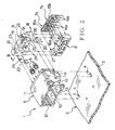
- the receptacle 1 is attached to a printed circuit board 2 (PCB) of various electronic equipment as an auxiliary device as described above.
- the printed circuit board 2 is one of the external electronic parts as described above.
- the printed circuit board 2 has an insulating substrate 3, and a not-shown conductive pattern formed on said substrate 3.
- the conductive pattern is made of conductive metal such as copper, formed in a thin film, and stuck on a surface of the substrate 3.
- a slit 4 with which a latter described earth terminal 20 is engaged, and not-shown holes, through which lead terminals 16a, 16b are inserted, are formed on the printed circuit board 2. These slit 4 and holes 16a, 16b penetrate the printed circuit board 2.
- the optical plug is inserted into the engaging chamber 13.
- the engaging chamber 13 is engaged with the optical plug.
- the container receives the optical receiving device 7a, the optical transmitting device 7b, the module case 8, and one end near the optical plug of a later described holder 19 of the shield case 9.
- the housing 5 includes a not-shown pair of receiving tubes formed on the back wall.
- Each of said pair of receiving tubes has a cylinder-like shape, of which an inner diameter is substantially equal to an outer diameter of the sleeve 6.
- the pair of receiving tubes is continued to the back wall, and penetrates the back wall. Further, each receiving tube communicates the engaging chamber 13 to the container.
- the housing 5 includes a pair of sockets 14, into which an earth terminal is pressed.
- Said sockets 14 are provided on each outer surface of a pair of side walls 12 of the housing 5. Later described earth terminals 20 of the shield case 9 are press-fitted into the sockets 14.
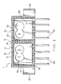
- the optical receiving device 7a and the optical transmitting device 7b are received by the container, while respectively being received by the module case 8.
- the optical receiving device 7a converts the received light to an electrical, and includes a main body 15a received by the module case 8 and a plurality of lead terminals 16a.
- the main body 15a has a flat, plate-like shape with a rectangular shape in a plane view.
- the main body 15a includes a photoelectric converter for receiving the signal light.
- the photoelectric converter faces an end surface of the optical fiber of the optical plug engaged with the housing 5.
- the photoelectric converter converts the signal light received through the optical fiber cable into an electrical signal.
- the optical transmitting device 7b is a device to convert an electrical signal into signal light, and includes a main body 15b received by the module case 8 and a plurality of lead terminals 16b.
- the main body 15b has a flat plate-like shape with a rectangular shape in a plane view.
- the main body 15b includes a photoelectric converter to receive signal light.
- the photoelectric converter faces the end surface of the optical fiber cable of the optical plug.
- the photoelectric converter converts the electric light into the signal light.
- the lead terminal 16b is continued to the main body 15b, and the lead terminal 16b is protruded from the main body 15b.
- the lead terminal 16b is electrically connected to the photoelectric converter.
- the lead terminal 16b is protruded outward (below) from the bottom wall 10 of the housing 5.
- the lead terminal 16b is electrically connected to the conductive pattern of the printed circuit board 2.
- the lead terminals 16a, 16b are arranged (passed through) respectively inside the notches 17. Therefore, when the module case 8 receives the main bodies 15a, 15b, spaces 18 between the notches 17 adjacent to each other are arranged in between the adjacent lead terminals 16a, 16b.
- the module case 8 includes the locating parts located respectively in between the lead terminals 16a, 16b adjacent to each other.
- the shield case 9 is formed by such as bending conductive sheet metal. Namely, the shield case 9 has conductivity. As shown in Fig. 2, the shield case 9 integrally includes a holder 19 having a flat box-like shape and a pair of earth terminals 20. Since the shield case 9 includes the holder 19, the shield case 9 is described to have a box-like shape in this specification. In addition to receiving the module 8, as shown in Figs. 3 and 4, the holder 19 includes a first holder 21, a second holder 22, a partition wall 23 formed in between the first and second holders 21, 22, and an overlapping part 24 (shown in Figs. 6 and 7).
- the first holder 21 and the second holder 22 include a flat box-like shape having an opening 25 at a bottom in the Fig. 2.
- the opening 25 is an opening to make interiors of the holders 21, 22 communicate with exteriors of the holders 21, 22.
- the first holder 21 and the second holder 22 are arranged along a line in which the main bodies 15a, 15b of the optical receiving and transmitting devices 7a, 7b are arranged.
- holder 19 having the above described structure receives the module case 8
- one end at a near side in Fig. 2 of said holder 19 is received in the container of the housing 5. Further, the other end at a far side in Fig. 2 of the holder 19 is exposed to an exterior of the housing 5.
- the partition wall 23 extends in a direction that the module case 8 is inserted into the first and second holders 21, 22 through the opening 25.
- the partition wall 23 partitions a room inside the holder 19 into the first and second holders 21, 22.
- the overlapping part 24 is formed across the first and second holders 21, 22.
- the overlapping part 24 is formed at sleeves 6 side of the holder 19 at a near side in Fig. 2, namely, at the optical plug side. Further, the overlapping part 24 is formed at an edge near the printed circuit board 2, which is arranged at a bottom end in Fig. 2, of the first and second holders 21, 22.
- the overlapping part 24 is formed by a part of one sheet 21a of sheet metal forming the first holder 21, and a part of the other sheet 22a of sheet metal forming the second holder 22, said parts overlapping with each other. Further, said parts of the sheet metals 21a, 22a are in contact with each other at the overlapping part 24.
- the pair of earth terminals 20 is inserted into and engaged with the slits 4 on the printed circuit board 2 to be connected to the conductive pattern of the printed circuit board 2.
- the pair of earth terminals 20 is fixed on the printed circuit board 2 by such as being engaged with the printed circuit board 2.
- the pair of earth terminals 20 electrically connects the shield case 9 to the conductive pattern of the printed circuit board 2.
- the pair of earth terminals 20 electrically connects the shield case 9 to such as an earth circuit through the conductive pattern of the printed circuit board 2. Further, the pair of earth terminals 20 is pressed into sockets 14 to fix the shield case 9 to the housing 5.
- a locking hook 26 for locking the pair of earth terminals 20 in the sockets 14 is formed on the respective earth terminals 20 integrally.
- the shield case 9 presses the sleeves 6 toward the back of the light receiving tubes, namely the back of the housing 5.
- the optical receiving and transmitting devices 7a, 7b are arranged in suitable positions.
- the receptacle 1 is assembled.
- the optical plug is allowed to engage with the receptacle 1.
- the bottom wall 10 is placed on the printed circuit board 2.
- the pair of earth terminals 20 and the lead terminals 16a, 16b are inserted into the slits 4 and the holes on the printed circuit board 2. While the pair of earth terminals 20 is engaged with the slits 4 and connected electrically to the conductive pattern on the printed circuit board 2, the lead terminals 16a, 16b penetrating through the holes are fixed on the conductive pattern of the printed circuit board 2 by such as soldering. thus, the receptacle 1 is attached to the printed circuit board 2.
- the receptacle 1 After the receptacle 1 is attached to the printed circuit board 2, when the optical plug is engaged with the receptacle 1, an electrical signal is supplied to the optical transmitting device 7b through the conductive pattern of the printed circuit board 2.
- the receptacle 1 converts the electrical signal to signal light, and emits the signal light toward one of the optical fibers of the optical plug.
- the receptacle 1 signal light is inputted into the optical receiving device 7a from the other optical fiber of the optical plug.
- the receptacle 1 converts the signal light received by the optical receiving device 7a to an electrical signal, and supplies the electrical signal to the conductive patterns on the printed circuit board 2 through the lead terminal 16a.
- the receptacle 1 converts the signal light from the optical plug to the electrical signal to supply to the printed circuit board 2, and converts the electrical signal from the printed circuit board 2 to the signal light to supply to the optical plug.
- the receptacle 1 discharges electrical noise, which is to intrude into the optical receiving and transmitting devices 7a, 7b from outside, into the earth circuit through the holder 19 of the shield case 9 and the pair of earth terminals 20.
- the receptacle 1 also discharges electrical noise, which is generated by the optical receiving and transmitting devices 7a, 7b, into the earth circuit through the holder 19 of the shield case 9 and the pair of earth terminals 20.
- the external electrical noise is prevented from intruding into the optical receiving and transmitting devices 7a, 7b, and the electrical noise, generated by the optical receiving and transmitting devices 7a, 7b, is prevented from being emitted outward.
- the shield case 9 only receives the module case 8, which receives the main bodies 15a, 15b of the optical receiving and transmitting devices 7a, 7b. Therefore, the opening 25 of the shield case 9 can be made smaller. Therefore, it is hard for the external electrical noise to intrude into the optical receiving and transmitting devices 7a, 7b through the opening 25 of the shield case 9. Further, it is hard for the electrical noise, generated by the optical receiving and transmitting devices 7a, 7b, to be emitted outward through the opening 25. Therefore, the external electrical noise is prevented from intruding into the optical receiving and transmitting devices 7a, 7b, and the electrical noise, generated by the optical receiving and transmitting devices 7a, 7b, can be prevented from being emitted outward.
- Each of locating parts 18 of the module case 8 is located in between the terminals adjacent to each other of the lead terminals 16a, 16b. Therefore, when the lead terminals 16a, 16b start to move in the module case 8, they are blocked by the locating parts 18 to be prevented from moving in the module case 8.
- the lead terminals 16a, 16b can be prevented from rattling in the module case 8, namely in the housing 5, and an electrical connection between these lead terminals 16a, 16b and the printed circuit board 2 as one of external electronic parts can be prevented from being unstable. Therefore, the optical receiving and transmitting devices 7a, 7b can be connected electrically and reliably to the printed circuit board 2. Further, the locating parts 18 prevent the lead terminals 16a, 16b from being in contact with each other. Therefore, the locating parts 18 prevent the lead terminals 16a, 16b from being short-circuited to each other.
- the partition wall 23 is formed on the shield case 9. Therefore, electrical noise, which is generated by electrical signal outputted from the optical receiving device 7a to the printed circuit board 2, is prevented from intruding into the optical transmitting device 7b. Further, electrical noise, which is generated by electrical signal inputted into the optical transmitting device 7b, is prevented from intruding into the optical receiving device 7a. Therefore, electrical noises of the optical receiving and transmitting devices 7a, 7b affecting each other can be reduced to improve cross-talk characteristics of the receptacle 1.
- the receptacle 1 can prevent electrical noise from being emitted outward from an overlapping part 24 where the sheet metals 21a, 22a, forming these holders 21, 22 respectively, overlap with each other. Therefore, the receptacle 1 can reliably prevent the electric noise generated by the optical receiving and transmitting devices 7a, 7b from being emitted outward.
Landscapes
- Physics & Mathematics (AREA)
- General Physics & Mathematics (AREA)
- Optics & Photonics (AREA)
- Electromagnetism (AREA)
- Optical Couplings Of Light Guides (AREA)
- Mechanical Coupling Of Light Guides (AREA)
Priority Applications (1)
| Application Number | Priority Date | Filing Date | Title |
|---|---|---|---|
| EP08017825A EP2017661A1 (fr) | 2003-07-03 | 2004-05-25 | Connecteur optique pour réduire le bruit |
Applications Claiming Priority (2)
| Application Number | Priority Date | Filing Date | Title |
|---|---|---|---|
| JP2003190904A JP4256728B2 (ja) | 2003-07-03 | 2003-07-03 | 光コネクタ |
| JP2003190904 | 2003-07-03 |
Related Child Applications (2)
| Application Number | Title | Priority Date | Filing Date |
|---|---|---|---|
| EP08017825A Division EP2017661A1 (fr) | 2003-07-03 | 2004-05-25 | Connecteur optique pour réduire le bruit |
| EP08017825.4 Division-Into | 2008-10-10 |
Publications (3)
| Publication Number | Publication Date |
|---|---|
| EP1494051A2 true EP1494051A2 (fr) | 2005-01-05 |
| EP1494051A3 EP1494051A3 (fr) | 2006-01-11 |
| EP1494051B1 EP1494051B1 (fr) | 2012-12-12 |
Family
ID=33432341
Family Applications (2)
| Application Number | Title | Priority Date | Filing Date |
|---|---|---|---|
| EP08017825A Withdrawn EP2017661A1 (fr) | 2003-07-03 | 2004-05-25 | Connecteur optique pour réduire le bruit |
| EP04012338A Expired - Lifetime EP1494051B1 (fr) | 2003-07-03 | 2004-05-25 | Connecteur optique pour la réduction du bruit |
Family Applications Before (1)
| Application Number | Title | Priority Date | Filing Date |
|---|---|---|---|
| EP08017825A Withdrawn EP2017661A1 (fr) | 2003-07-03 | 2004-05-25 | Connecteur optique pour réduire le bruit |
Country Status (3)
| Country | Link |
|---|---|
| US (1) | US7104705B2 (fr) |
| EP (2) | EP2017661A1 (fr) |
| JP (1) | JP4256728B2 (fr) |
Families Citing this family (10)
| Publication number | Priority date | Publication date | Assignee | Title |
|---|---|---|---|---|
| KR100456272B1 (ko) * | 2002-11-13 | 2004-11-09 | 양관숙 | 광접속모듈 |
| JP2005006228A (ja) * | 2003-06-13 | 2005-01-06 | Casio Comput Co Ltd | プロジェクタ |
| US7128475B2 (en) * | 2004-10-28 | 2006-10-31 | Schweitzer Engineering Laboratories, Inc. | Fiber optic connector |
| JP4413238B2 (ja) * | 2007-03-02 | 2010-02-10 | 株式会社オートネットワーク技術研究所 | 車両用ネットワークシステム |
| JP5095579B2 (ja) * | 2008-10-24 | 2012-12-12 | 矢崎総業株式会社 | 光コネクタ |
| JP5162500B2 (ja) | 2009-03-06 | 2013-03-13 | アルプス電気株式会社 | シールドを有する光コネクタ |
| JP5690510B2 (ja) * | 2010-06-28 | 2015-03-25 | 矢崎総業株式会社 | 電子部品 |
| JP2012053246A (ja) * | 2010-09-01 | 2012-03-15 | Auto Network Gijutsu Kenkyusho:Kk | 基板実装型の光コネクタ |
| JP5727259B2 (ja) * | 2011-02-28 | 2015-06-03 | 矢崎総業株式会社 | 光モジュール |
| JP2017009727A (ja) * | 2015-06-19 | 2017-01-12 | 矢崎総業株式会社 | 光コネクタ |
Family Cites Families (10)
| Publication number | Priority date | Publication date | Assignee | Title |
|---|---|---|---|---|
| FR2652229B1 (fr) * | 1989-09-19 | 1991-11-15 | Bull Sa | Ensemble de blindage pour un bloc collecteur relie a un equipement electrique place a l'interieur d'un chassis. |
| US6213651B1 (en) | 1999-05-26 | 2001-04-10 | E20 Communications, Inc. | Method and apparatus for vertical board construction of fiber optic transmitters, receivers and transceivers |
| JP3646979B2 (ja) * | 1999-12-08 | 2005-05-11 | 矢崎総業株式会社 | ハイブリッドコネクタ |
| JP2001147346A (ja) | 1999-11-19 | 2001-05-29 | Yazaki Corp | 雌コネクタ |
| US6499889B1 (en) | 1999-12-08 | 2002-12-31 | Yazaki Corporation | Method of assembling optical connector, optical connector and hybrid connector |
| JP2002023027A (ja) | 2000-07-07 | 2002-01-23 | Yazaki Corp | 光コネクタ |
| JP4299958B2 (ja) * | 2000-07-31 | 2009-07-22 | 富士通株式会社 | 通信装置及びプラグインユニット |
| JP4550268B2 (ja) | 2000-12-20 | 2010-09-22 | 古河電気工業株式会社 | 光・電気複合コネクタ |
| US6607308B2 (en) * | 2001-02-12 | 2003-08-19 | E20 Communications, Inc. | Fiber-optic modules with shielded housing/covers having mixed finger types |
| JP4494668B2 (ja) | 2001-04-27 | 2010-06-30 | 古河電気工業株式会社 | コネクタ |
-
2003
- 2003-07-03 JP JP2003190904A patent/JP4256728B2/ja not_active Expired - Fee Related
-
2004
- 2004-05-18 US US10/847,458 patent/US7104705B2/en not_active Expired - Fee Related
- 2004-05-25 EP EP08017825A patent/EP2017661A1/fr not_active Withdrawn
- 2004-05-25 EP EP04012338A patent/EP1494051B1/fr not_active Expired - Lifetime
Also Published As
| Publication number | Publication date |
|---|---|
| JP4256728B2 (ja) | 2009-04-22 |
| EP2017661A1 (fr) | 2009-01-21 |
| JP2005024944A (ja) | 2005-01-27 |
| EP1494051A3 (fr) | 2006-01-11 |
| US7104705B2 (en) | 2006-09-12 |
| US20050002620A1 (en) | 2005-01-06 |
| EP1494051B1 (fr) | 2012-12-12 |
Similar Documents
| Publication | Publication Date | Title |
|---|---|---|
| US6783283B2 (en) | Optical connector for coupling optical signals to optical devices | |
| JP3646979B2 (ja) | ハイブリッドコネクタ | |
| EP1217407B1 (fr) | Connecteur composé optique/électrique | |
| US6357931B1 (en) | Hybrid connector | |
| JP3735011B2 (ja) | ハイブリッドコネクタの組み付け方法 | |
| EP1170612B1 (fr) | Connecteur hybride optique et électrique | |
| US7111994B2 (en) | Integral insert molded fiber optic transceiver electromagnetic interference shield | |
| EP1494051B1 (fr) | Connecteur optique pour la réduction du bruit | |
| JP2015500517A (ja) | 光モジュール | |
| JP3778479B2 (ja) | 発光素子モジュール及び受光素子モジュールの位置決め方法、光コネクタ、及びハイブリッドコネクタ | |
| US7090410B2 (en) | Optical receptacle with low transmission loss and photoelectric conversion module for the same | |
| CN102365569B (zh) | 光连接器 | |
| EP1256828B1 (fr) | Dispositif connecteur et connecteur | |
| JP3654574B2 (ja) | ハイブリッドコネクタの支持構造 | |
| JP2002023026A (ja) | 光コネクタ | |
| CN111108421B (zh) | 光学连接器装置 | |
| JP2002023025A (ja) | 光コネクタ | |
| US10151889B2 (en) | Optical connector and branch structure of wire harness | |
| JP2002023027A (ja) | 光コネクタ | |
| EP1102099A2 (fr) | Connecteur hybride | |
| TWM679044U (zh) | 光電適配器 | |
| JP2002182075A (ja) | 光コネクタの嵌合構造 | |
| WO2020111182A1 (fr) | Câble et système de transmission d'image | |
| WO2007069296A1 (fr) | Fiche de connexion pour guide d'onde optique |
Legal Events
| Date | Code | Title | Description |
|---|---|---|---|
| PUAI | Public reference made under article 153(3) epc to a published international application that has entered the european phase |
Free format text: ORIGINAL CODE: 0009012 |
|
| AK | Designated contracting states |
Kind code of ref document: A2 Designated state(s): AT BE BG CH CY CZ DE DK EE ES FI FR GB GR HU IE IT LI LU MC NL PL PT RO SE SI SK TR |
|
| AX | Request for extension of the european patent |
Extension state: AL HR LT LV MK |
|
| PUAL | Search report despatched |
Free format text: ORIGINAL CODE: 0009013 |
|
| AK | Designated contracting states |
Kind code of ref document: A3 Designated state(s): AT BE BG CH CY CZ DE DK EE ES FI FR GB GR HU IE IT LI LU MC NL PL PT RO SE SI SK TR |
|
| AX | Request for extension of the european patent |
Extension state: AL HR LT LV MK |
|
| 17P | Request for examination filed |
Effective date: 20060209 |
|
| AKX | Designation fees paid |
Designated state(s): DE |
|
| RAP1 | Party data changed (applicant data changed or rights of an application transferred) |
Owner name: YAZAKI CORPORATION |
|
| GRAP | Despatch of communication of intention to grant a patent |
Free format text: ORIGINAL CODE: EPIDOSNIGR1 |
|
| GRAS | Grant fee paid |
Free format text: ORIGINAL CODE: EPIDOSNIGR3 |
|
| GRAA | (expected) grant |
Free format text: ORIGINAL CODE: 0009210 |
|
| AK | Designated contracting states |
Kind code of ref document: B1 Designated state(s): DE |
|
| REG | Reference to a national code |
Ref country code: DE Ref legal event code: R096 Ref document number: 602004040360 Country of ref document: DE Effective date: 20130207 |
|
| PLBE | No opposition filed within time limit |
Free format text: ORIGINAL CODE: 0009261 |
|
| STAA | Information on the status of an ep patent application or granted ep patent |
Free format text: STATUS: NO OPPOSITION FILED WITHIN TIME LIMIT |
|
| 26N | No opposition filed |
Effective date: 20130913 |
|
| REG | Reference to a national code |
Ref country code: DE Ref legal event code: R097 Ref document number: 602004040360 Country of ref document: DE Effective date: 20130913 |
|
| PGFP | Annual fee paid to national office [announced via postgrant information from national office to epo] |
Ref country code: DE Payment date: 20140521 Year of fee payment: 11 |
|
| REG | Reference to a national code |
Ref country code: DE Ref legal event code: R119 Ref document number: 602004040360 Country of ref document: DE |
|
| PG25 | Lapsed in a contracting state [announced via postgrant information from national office to epo] |
Ref country code: DE Free format text: LAPSE BECAUSE OF NON-PAYMENT OF DUE FEES Effective date: 20151201 |