EP1495512B1 - Eingebetteter planarer zirkulator und verfahren zu seiner herstellung - Google Patents
Eingebetteter planarer zirkulator und verfahren zu seiner herstellung Download PDFInfo
- Publication number
- EP1495512B1 EP1495512B1 EP03723954A EP03723954A EP1495512B1 EP 1495512 B1 EP1495512 B1 EP 1495512B1 EP 03723954 A EP03723954 A EP 03723954A EP 03723954 A EP03723954 A EP 03723954A EP 1495512 B1 EP1495512 B1 EP 1495512B1
- Authority
- EP
- European Patent Office
- Prior art keywords
- circulator
- assembly
- disposed
- sub
- port
- Prior art date
- Legal status (The legal status is an assumption and is not a legal conclusion. Google has not performed a legal analysis and makes no representation as to the accuracy of the status listed.)
- Expired - Lifetime
Links
- 238000000034 method Methods 0.000 title claims description 28
- 229910000859 α-Fe Inorganic materials 0.000 claims abstract description 65
- 238000000429 assembly Methods 0.000 claims abstract description 38
- 239000000758 substrate Substances 0.000 claims abstract description 10
- 230000005540 biological transmission Effects 0.000 claims description 12
- 230000001629 suppression Effects 0.000 claims description 12
- RYGMFSIKBFXOCR-UHFFFAOYSA-N Copper Chemical compound [Cu] RYGMFSIKBFXOCR-UHFFFAOYSA-N 0.000 claims description 8
- 229910052802 copper Inorganic materials 0.000 claims description 8
- 239000010949 copper Substances 0.000 claims description 8
- 238000007747 plating Methods 0.000 claims description 7
- 229910000831 Steel Inorganic materials 0.000 claims description 5
- 239000010959 steel Substances 0.000 claims description 5
- 239000012815 thermoplastic material Substances 0.000 claims description 5
- 238000005553 drilling Methods 0.000 claims description 3
- 230000008878 coupling Effects 0.000 claims 2
- 238000010168 coupling process Methods 0.000 claims 2
- 238000005859 coupling reaction Methods 0.000 claims 2
- 239000000463 material Substances 0.000 description 20
- 230000000712 assembly Effects 0.000 description 16
- 238000003475 lamination Methods 0.000 description 10
- 229920001343 polytetrafluoroethylene Polymers 0.000 description 9
- 239000004810 polytetrafluoroethylene Substances 0.000 description 9
- 238000004519 manufacturing process Methods 0.000 description 8
- 238000003491 array Methods 0.000 description 6
- 238000004891 communication Methods 0.000 description 5
- 239000000853 adhesive Substances 0.000 description 3
- 238000004026 adhesive bonding Methods 0.000 description 3
- 230000001070 adhesive effect Effects 0.000 description 3
- 238000010586 diagram Methods 0.000 description 3
- 230000000694 effects Effects 0.000 description 3
- 229910052751 metal Inorganic materials 0.000 description 3
- 239000002184 metal Substances 0.000 description 3
- 238000012545 processing Methods 0.000 description 3
- 229910000938 samarium–cobalt magnet Inorganic materials 0.000 description 3
- 229910000679 solder Inorganic materials 0.000 description 3
- 229920001169 thermoplastic Polymers 0.000 description 3
- 229920001187 thermosetting polymer Polymers 0.000 description 3
- 239000004416 thermosoftening plastic Substances 0.000 description 3
- 239000004812 Fluorinated ethylene propylene Substances 0.000 description 2
- -1 Polytetrafluoroethylene Polymers 0.000 description 2
- KPLQYGBQNPPQGA-UHFFFAOYSA-N cobalt samarium Chemical compound [Co].[Sm] KPLQYGBQNPPQGA-UHFFFAOYSA-N 0.000 description 2
- 238000005516 engineering process Methods 0.000 description 2
- 239000000155 melt Substances 0.000 description 2
- 229920009441 perflouroethylene propylene Polymers 0.000 description 2
- 238000000926 separation method Methods 0.000 description 2
- 230000003068 static effect Effects 0.000 description 2
- 239000004593 Epoxy Substances 0.000 description 1
- 230000002411 adverse Effects 0.000 description 1
- 238000013459 approach Methods 0.000 description 1
- 238000007796 conventional method Methods 0.000 description 1
- 238000013461 design Methods 0.000 description 1
- 238000011438 discrete method Methods 0.000 description 1
- 125000003700 epoxy group Chemical group 0.000 description 1
- HQQADJVZYDDRJT-UHFFFAOYSA-N ethene;prop-1-ene Chemical group C=C.CC=C HQQADJVZYDDRJT-UHFFFAOYSA-N 0.000 description 1
- 239000002223 garnet Substances 0.000 description 1
- PCHJSUWPFVWCPO-UHFFFAOYSA-N gold Chemical compound [Au] PCHJSUWPFVWCPO-UHFFFAOYSA-N 0.000 description 1
- 239000010931 gold Substances 0.000 description 1
- 229910052737 gold Inorganic materials 0.000 description 1
- 230000005415 magnetization Effects 0.000 description 1
- 238000002844 melting Methods 0.000 description 1
- 238000004806 packaging method and process Methods 0.000 description 1
- 230000003071 parasitic effect Effects 0.000 description 1
- 229920000647 polyepoxide Polymers 0.000 description 1
- 238000005476 soldering Methods 0.000 description 1
Images



Classifications
-
- H—ELECTRICITY
- H01—ELECTRIC ELEMENTS
- H01P—WAVEGUIDES; RESONATORS, LINES, OR OTHER DEVICES OF THE WAVEGUIDE TYPE
- H01P1/00—Auxiliary devices
- H01P1/32—Non-reciprocal transmission devices
- H01P1/38—Circulators
- H01P1/383—Junction circulators, e.g. Y-circulators
- H01P1/387—Strip line circulators
Definitions
- This invention relates generally to communications systems and, more particularly, to planar circulators and methods of fabrication.
- a radar or communications system antenna generally includes a feed circuit and at least one conductive member generally referred to as a reflector or radiator.
- an array antenna can include a plurality of radio frequency (RF) circulators disposed in an array in a manner in which RF signals can be received from or transmitted to the same individual radiator. Sharing the radiators for both transmitting and receiving signals allows a reduction in the size of the antenna in applications where simultaneous transmission and reception is not required.
- the circulators are also referred to as transmit/receive (T/R) elements.
- the radio frequency (RF) circulator is a three-port device, having a first, a second, and a third port.
- a conventional circulator provides a directional capability so that an RF signal applied as an input to the first port provides an output signal at only the second port.
- an RF signal applied as an input to the second port provides an output signal at only the third port
- an RF signal applied as an input to the third port provides an output signal at only the first port.
- Conventional circulators are typically provided as discrete devices that can be mounted to a circuit board. Since it contains discrete devices, the conventional circulator does not provide an optimal form factor for high density electronics packaging. In commercial applications, it is often desirable to integrate RF circuits into low profile, low cost packages. For example such devices would be desirable for commercial cell phones. In military surface and airborne applications, there is a need for tile arrays having multiple board layers. Further, in these applications there is a need for low profile, low cost arrays which often require a large number of circulators for corresponding radiators. In conventional systems the circulators are often individually packaged in the transmitter/receiver (T/R) modules thereby increasing module cost and increasing the unit cell footprint so as to reduce an array scan volume versus frequency characteristic due to interference from adjacent lobes in the antenna pattern.
- T/R transmitter/receiver
- One conventional method includes steps for fabricating individual circulators having gaussed (i.e. magnetized) magnets and embedding each individual circulator in a dielectric or metal carrier.
- This method requires precise alignment and ribbon (or wire) bonding to complete the RF circuit.
- the gaussed magnets must be individually magnetized and are exposed to high lamination temperatures during fabrication. Consequently, the magnets experience partial de-magnetization causing a non-uniform magnetization adversely affecting circulator performance. This effect is a function of magnet location across the array. Embedding each individual circulator in a dielectric or metal carrier requires precise individual alignment between the circulator transmission line ports and the carrier transmission line ports.
- Ribbon (or wire) bonding between circulator transmission lines and board transmission lines to complete an RF circuit requires special plating (e.g., gold plating) for soldering or bonding. Consequently, the RF bandwidth is reduced and signal losses are increased due to process variations that add parasitic reactances to the RF transmission line.
- plating e.g., gold plating
- a planar circulator assembly includes a dielectric substrate having a first surface and an opposing second surface, a plurality of circulator circuits each having a first ferrite receiving pad disposed on the first surface and a second ferrite receiving pad disposed on the second surface a first sub-assembly board.
- the first sub-assembly board is disposed on the first surface, has a plurality of first apertures, a plurality of ferrite-magnet sub-assemblies, each ferrite-magnet sub-assembly disposed in a corresponding first aperture and aligned with a corresponding first ferrite receiving pad and electromagnetically coupled to the corresponding first ferrite receiving pad.
- the assembly further includes a second sub-assembly board disposed on the second surface having a plurality of second apertures, and a plurality of ferrites each disposed in a corresponding second aperture aligned with a corresponding second ferrite receiving pad and electromagnetically coupled to the corresponding second ferrite receiving pad.
- This arrangement eliminates fabrication of individual circulators by embedding each individual circulator in a dielectric or metal carrier. Such an arrangement further eliminates precise alignment and ribbon (or wire) bonding for attaching circulators in fixed orientations to complete the RF circuit by using epoxies and/or solders. With such an arrangement, a plurality of low-profile circulators are embedded in a multi-layer laminate in one bonding step using standard Printed Wiring Board (PWB) and Surface Mount Technology (SMT) processes, for example this arrangement reduces the antenna unit cell spacing by reducing the T/R module footprint in order to provide a larger radar scan volume.
- PWB Printed Wiring Board
- SMT Surface Mount Technology
- a planar circulator assembly includes at least one first RF port via disposed in the first sub-assembly board, each first RF port via having a first end coupled to a corresponding one of the first, second and third ports and a second end coupled to a connection disposed on a first outer surface of the circulator assembly.
- the planar circulator assembly further includes at least one second RF port via disposed in the second sub-assembly board, each second RF via having a first end coupled to one of the first, second and third ports and a second end coupled to a connection disposed on a second outer surface of the circulator assembly disposed opposite the first outer surface.
- a method for making an embedded planar circulator assembly includes providing a circulator board having a first surface and an opposing second surface, forming a plurality of circulator circuits disposed on the circulator board, each circuit having a ferrite receiving pad disposed on the first surface and a corresponding ferrite receiving pad on the second surface, providing a plurality of ferrite-magnet sub-assemblies disposed in a first sub-assembly.
- the method further includes providing a plurality of ferrites disposed in a second sub-assembly, and bonding the circulator board between the first sub-assembly and the second sub-assembly such that the ferrite-magnet sub-assemblies are urged against a corresponding ferrite receiving pad disposed on the first surface of the circulator board and the ferrites are urged against the corresponding ferrite receiving pad on the second surface of the circulator board.
- a method for making an embedded planar circulator assembly further includes separating the plurality of circulator circuits into a corresponding plurality of individual unit cells.
- phased arrays have precluded the use of phased arrays in all but the most specialized applications. Assembly and component costs (especially the active transmit/receive module including circulators) are major cost drivers. Phased array costs can be reduced by leveraging batch processing and minimizing touch labor of components and assemblies.
- the circulators which are typically discrete components wired into T/R modules, are embedded in Polytetrafluoroethylene (PTFE) dielectric laminates, thus reducing cost and complexity in the T/R modules.
- PTFE Polytetrafluoroethylene
- the size of the unit cell of a phased array is reduced by including the array of circulators in a single planar assembly.
- the embedded planar circulator is fabricated with high temperature bonding adhesives common to the PWB industry and the circulator magnets are conveniently magnetized after bonding. The result is a compact, sealed, low cost and high performance array of circulators in a planar array arrangement. Individual circulators are produced in volume by spacing a plurality of circulators on a single circulator board to facilitate separation into individual unit cells.
- the array antenna including a radiating element of a particular type, size and shape.
- one type of radiating element is a so-called patch antenna element having a square shape and a size compatible with operation at a particular frequency (e.g. 10 GHz).
- a particular frequency e.g. 10 GHz
- Those of ordinary skill in the art will recognize, of course that other shapes and types of antenna elements may also be used and that the size of one or more radiating elements may be selected for operation at any frequency in the RF frequency range (e.g. any frequency in the range of about 1 GHz to about 100 GHz).
- the types of radiating elements which may be used in the antenna of the present invention include but are not limited to notch elements, dipoles, slots or any other radiating element known to those of ordinary skill in the art which can be coupled to a circulator.
- the radar or communication system 100 includes an antenna array 16 having a plurality of radiating elements 12a-12n (generally referred to as radiating elements 12).
- the embedded planar circulator assembly 10 includes a plurality of transmit/receive (T/R) modules 14a-14n (generally referred to as T/R modules 14).
- the radiating elements 12 are coupled to corresponding T/R modules 14a-14n, each of which is coupled to a plurality of amplifiers 24a-24n and a plurality of phase shifters 22a-22n in the transmit path and a plurality of amplifiers 20a-20n, a plurality of attenuators 26a-26n and a plurality of phase shifters 28a-28n in the receive path, respectively.
- the T/R modules 14 can be shared by the radiating elements of both a sum channel beamformer (not shown) and a difference channel beamformer (not shown), for example.
- an embedded planar circulator assembly 10 includes an upper board sub-assembly 40 disposed on a circulator circuit board 42, which is disposed on a lower board sub-assembly 44.
- the upper board sub-assembly 40 includes a plurality of recessed two-step cavities 46 adapted to receive a plurality of ferrite-magnet sub-assemblies 48, which includes a magnet 50 disposed on a ferrite 52.
- the upper board sub-assembly 40 further includes a plurality of antenna port vias 62 adapted to connect to a plurality of radiators (not shown).
- the circulator circuit board 42 comprises a plurality of circulator board unit cells 54a-54n (generally referred to as unit cells 54), which are coupled to the plurality of antenna port vias 62 and to the plurality of ferrite-magnet sub-assemblies.
- the lower board sub-assembly 44 includes a plurality of recessed cavities 58 adapted to receive a plurality of ferrite-pole piece assemblies 59.
- the plurality of ferrite-pole piece assemblies 59 include a plurality of ferrites 56 disposed on a corresponding plurality of pole pieces 57, here for example steel pole pieces 57 which have approximately the same diameter of the ferrite 56 and are bonded to each of the ferrites 56.
- the lower board sub-assembly 44 further includes a plurality of receive port vias 64 and transmit port vias 66 which are adapted to couple receive and transmit feed circuits (not shown) to respective ports on the plurality of circulator board unit cells 54.
- the circulator circuits include etched copper circuits on both sides of a copper clad PTFE (Polytetrafluoroethylene) substrate, for example Rogers 3010 (a high frequency circuit material manufactured by Rogers corporation), and the upper and lower upper board sub-assembly 40 and 44 are fabricated from PTFE.
- a copper clad PTFE Polytetrafluoroethylene
- the ferrite 52 material is includes Garnet and the magnet 50 material includes Samarium Cobalt (SmCo).
- SmCo Samarium Cobalt
- the magnets 50 provide a static (DC) magnetic field to each circulator board unit cell 54 to induce circulator action.
- Table 1 Table 1.
- a circulator board unit cell 54 includes an upper surface circuit portion 68u and a corresponding lower surface circuit portion 68l separated by an insulating dielectric 43 of the circulator board 42.
- the upper surface circuit portion 68u includes a first port portion 70u coupled to an upper circulator junction 76u (also referred to as upper ferrite receiving pad) by a stripline circuit 84u.
- the upper circulator junction 76u is coupled to a second port portion 72u by a stripline circuit 86u and to a third port portion 74u by a further stripline circuit 82u.
- the first port portion 70u includes a connection 91 TX
- the second port portion 72u includes a connection 91 RX
- the third port portion 74u includes a connection 91 A .
- the lower surface circuit portion 68l includes a first port portion 70l coupled to a lower circulator junction 76l (also referred to as lower ferrite receiving pad 761) by a stripline circuit 84l.
- the lower circulator junction 76l is coupled to a second port portion 72l by a stripline circuit 861 and to a third port portion 74l by a further stripline circuit 82l.
- the first port portion 70l includes a connection 91 TX
- the second port portion 72l includes a connection 91 RX
- the third port portion 74l includes a connection 91 A .
- connections 91 RX , 91 TX , 91 A are coupled to plated RF vias 90 RX , 90 TX and 90 A when these vias are fabricated.
- the upper and lower surface circuits 68u, 68l and the upper and lower circulator junctions 76l, 76u include a plurality of interconnecting via connections 79a-79n (generally referred to as interconnecting via connections 79).
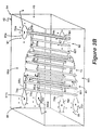
- FIG. 3B showing different elements of the circulator board unit cell 54 of FIG. 3A which are shown separately for clarity, a plurality of plated interconnecting vias 78a-78n connect the stripline circuits 82u, 84u, and 86u on the upper surface circuit 68u to corresponding circuit elements on the lower surface circuit 681.
- the plated interconnecting vias 78a-78n are coupled to the plurality of interconnecting via connections 79.
- the upper and lower surface circuits 68u, 681 are electrically interconnected with the plated interconnecting vias 78 forming an equivalent "thicker" RF circuit for each of the unit cells 54.
- the thicker RF circuits are referred to as transmission lines 82, 84 and 86 which are connected to the interconnected circulator junction 76u and 76l referred to as the circulator junction 76 or the ferrite receiving pad 76.
- the plated interconnecting vias 78a-78n are formed during fabrication of the circulator board 42 (described below in further detail in conjunction with step 202 of FIG. 7).
- the upper and lower surface circuits 68u, 681 include a plurality of mode suppression post connections 81.
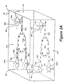
- FIG. 3C showing different elements of the circulator board unit cell 54 of FIG. 3A which are shown separately for clarity, a plurality of mode suppression posts 80 are disposed between the upper surface circuit portion 68u and the lower surface circuit portion 68l. For clarity, not all of the plurality of mode suppression posts 80 are shown.
- the RF circuit further includes a receive port RF via 90 RX , an antenna port RF via 90 A , and a transmit port RF via 90 TX (the three vias are generally referred to as RF vias 90) for each unit cell 54.
- FIG. 3C is shown for clarity without the plurality of plated interconnecting vias 78a-78n of FIG. 3B.
- the upper and lower surface circuits 68u and 68l are electrically interconnected with the plated RF vias 90 RX , 90 TX and 90 A forming an equivalent "thicker" RF circuit for each of the unit cells 54 and, in particular, form a first port 70, second port 72 and third port 74 connected to the circulator junction 76 (ferrite receiving pad 76) through transmission lines 82-86.
- the first port 70 is a transmit port
- the second port 72 is a receive port
- the third port 74 is an antenna port.
- an embedded planar isolator can be provided by terminating either the transmit RF port via 90 TX or the receive RF port via 90 RX in a resistive load.
- the RF vias 90 are disposed in the upper board sub-assembly 40,the circulator circuit board 42 and the lower board sub-assembly 44.
- the RF vias 90 A , 90 RX , 90 TX are not shown being terminated in connections on the outer surfaces of the upper board sub-assembly 40,and the lower board sub-assembly 44 respectively.
- the circulator board 42 includes a plurality of mode suppression posts 80 (FIG 3C) having first ends, for example, disposed in a circular pattern partially surrounding circuit portions 70u, 72u, 74u, and having second ends disposed in a circular pattern partially surrounding circuit portions 70l, 72l, 74l.
- the mode suppression posts 80 include plated vias coupled to ground planes 98, 99 (FIG. 4) to provide pseudo-coaxial RF transmission lines in combination with the corresponding port vias 90 for each RF port. For clarity, the mode suppression posts 80 are not shown being coupled to ground planes 98, 99.
- the RF vias 90 and mode suppression posts 80 are formed after the sub-assemblies have been bonded (described below in further detail in conjunction with steps 222-228).
- the upper surface circuit 68u and the corresponding lower surface circuit 681 are etched copper circuits
- the circulator board 42 is about .005 inches thick
- the connections 79, 81, 91 RX , 91 TX , 91 A are plated-thru holes
- the ferrite receiving pad 76 has a diameter of about 0.2 inches.
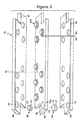
- FIG. 4 a cross section of FIG. 3A being taken along line 4-4 including the upper board sub-assembly 40 and the lower board sub-assembly 44 (FIG.2) is shown.
- An individual circulator unit cell 54 includes a magnet 50 disposed on a ferrite 52, which is disposed on a circulator circuit board 42.
- the unit cell 54 includes a pseudo-coaxial transmission line formed by antenna port 74u and 741 (FIG. 3C), plated interconnecting vias 78a-78n, mode suppression posts 80 and RF via 90 A which are coupled to the circulator junction 76 (FIG. 3B) by the stripline circuit 82 (FIG.
- the antenna port RF via 90 A includes a plated portion 92 A in the upper board sub-assembly 40 and a counter-drilled portion 94 A in the lower board sub-assembly 44.
- the receive port RF via 90 RX includes a plated portion 92 RX in the lower board sub-assembly 44 and a counter-drilled portion 94 RX in the upper board sub-assembly 40.
- the upper board sub-assembly 40 includes a ground plane 98 and the lower board sub-assembly 44 includes a further ground plane 99.
- the ground planes 98, 99 complete the stripline circuit formed by the upper surface circuit portion 68u and the lower surface circuit portion 68l.
- the transmit port RF via includes a plated portion (not shown) in the lower board sub-assembly 44 and a counter-drilled portion (not shown) in the upper board sub-assembly 40.
- received signals are coupled from an antenna radiator (not shown) through the antenna port RF via 90 A through the stripline circuit 82 to the circulator junction 76 where the signals controlled by known circulator action are directed to the receive port RF via 90 RX through the stripline circuit 86.
- the receive port RF via 90 RX couples received signals to the receiver circuitry (not shown).
- Transmitted signals are coupled from the transmitter circuitry (not shown) to the transmit port RF via through the stripline circuit 84 to the circulator junction 76 where the signals controlled by known circulator action are directed through the stripline circuit 82 to the antenna port RF via 90 A which is coupled to the antenna radiator (not shown).
- an RF via 90 (which here represents either the receive or transmit RF via) includes a plated portion 92 substantially disposed in the lower board sub-assembly 44 and a counter-drilled portion 94.
- An upper interconnection 96u with the upper surface stripline circuit portion 68u and a lower interconnection 96lower with the lower surface stripline circuit 68l is formed when the via 90 is drilled out and plated.
- the RF via 90 is counter drilled to remove the plating in the counter-drilled portion 94 to eliminate any unwanted RF effects.
- antenna RF via plated portion 92 A is substantially disposed in the upper board sub-assembly 40 and FIG. 4A would be rotated 180 degrees to illustrate RF via plated portion 92 A .
- an upper board sub-assembly 40 before bonding, includes the plurality of cavities 46a -46n into which the plurality of ferrite-magnet sub-assemblies 48 are press fit.
- the ferrite-magnet sub-assemblies 48 stand proud (i.e. are taller than the cavities 46) of the upper board sub-assembly 40. After bonding under temperature and pressure, the ferrite-magnet sub-assemblies 48 are urged into contact with the circulator junction 76.
- a lower board sub-assembly 44 before bonding, includes the plurality of cavities 58a -58n into which the plurality of ferrite-pole piece assemblies 59 (FIG. 2) are press fit.
- the ferrite-pole piece assemblies 59 stand proud (i.e. are taller than the cavity 58) of the lower board sub-assembly 44.
- the ferrites 56 After bonding under temperature and pressure, the ferrites 56 are urged into contact with the ferrite receiving pad 76.
- FIG. 7 a flow diagram illustrates exemplary steps to fabricate the embedded planar circulator assembly 10 of FIG. 1.
- the procedure starts at step 200, then at step 202 interconnecting vias 78a -78n (FIG. 3) on circulator board 42 are drilled and plated.
- the circulator board is a 5-mil PTFE substrate and circuit etch tolerances of ⁇ 0.5-mils (typically associated with 0.5-oz. copper plating) are used.
- the upper surface circuit portion 68u (FIG. 3) and lower surface circuit 681 are imaged and etched on the circulator board 42 using known PWB techniques.
- the two circuit portions 68u, 681 are electrically connected by plated interconnecting vias 78a -78n that were formed in step 202.
- the ferrite-magnet sub-assemblies 48 are fabricated by bonding the magnets 50 onto ferrites 52.
- the magnets 50 and the ferrites 52 are soldered together using a high temperature solder. The magnets 50 do not have to be magnetized at this step in the process.
- the upper board sub-assembly 40 is fabricated using layers of PTFE material with cutouts in at least two layers in order to form the recessed two-step cavities 46 adapted to receive a plurality of ferrite-magnet sub-assemblies 48.
- the ferrite-magnet sub-assemblies 48 are press fit into the recessed two-step cavities 46 in order to securely retain the assemblies 48 until the bonding step 220.
- the assemblies 48 are press fit using pick and place assembly techniques.
- the two-step cavity 46 has a diameter and depth such that the ferrite-magnet sub-assembly fits securely and also stands proud of the cavity 46 in order to assure a reliable contact between the ferrite-magnet sub-assembly 48 and the ferrite receiving pad 76 after the planar circulator assembly 10 is bonded at step 220.
- the pole pieces 57 are bonded to the ferrites 56 to provide the ferrite-pole piece assembly 59 (FIG.2), for example, by using a high temperature solder.
- the lower board sub-assembly 44 is fabricated using layers of PTFE material with cutouts in at least one layer in order to form the recessed cavities 58 adapted to receive a plurality of ferrite-pole piece assemblies 59.
- the lower board sub-assembly is fabricated with recessed two-step cavity for an optional additional magnet.
- the ferrite-pole piece assemblies 59 are press fit into the recessed cavities 58 in order to securely retain the ferrite-pole piece assemblies 59 until the bonding step 220.
- the ferrite-pole piece assemblies 59 are press fit using pick and place assembly techniques.
- an additional magnet (not shown) is bonded to the ferrite-pole piece assembly 59 for improved bandwidth and lower loss for high performance applications.
- the lower board assembly 44 includes a recessed two-step cavity (not shown).
- upper and lower adhesive bonding sheets 41 and 45 having cutouts aligned with ferrite-magnet sub-assemblies 48 and the ferrite-pole piece assemblies 59 respectively are placed on each side of the circulator board 42.
- the adhesive bonding sheets 41 and 45 comprise a thermoplastic material such as fluorinated ethylene propylene (FEP).
- FEP fluorinated ethylene propylene
- Other materials widely used in the PWB industry, including but not limited to, thermoset materials such as Speedboard-C TM (manufactured by W. L. Gore & Associates, Inc.) can be used to provide the bonding sheets 41 and 45.
- the adhesive bonding sheets 41 and 45 are pre-drilled to allow direct contact between the ferrite disks and the ferrite-magnet sub-assemblies 48 with the circulator junctions in order to reduce RF signal loss.
- the two sub-assemblies 40 and 42 are aligned with the circulator board 42.
- alignment pins are used.
- the embedded planar circulator assembly 10 is bonded under temperature and pressure.
- the lamination cycle parameters range in temperature from about 250°F to about 650°F and in pressures from about 100psi to about 300psi depending on the particular materials used.
- High temperature thermoplastic adhesives are used in this step in order to provide flexibility in fabricating multi-layer stripline circuit assemblies.
- Multi-layer Printed Circuit Boards with complex architecture are often fabricated using sequential laminations. This technique requires creating sub-assemblies with multiple laminations, done in sequence, starting with the highest temperature bonding materials. The succeeding laminations are done at progressively lower temperatures to prevent the re-melting of the previously created bond lines.
- Exemplary materials used for the lamination of one layer to another include a thermoplastic and a thermoset material.
- Thermoset materials once they have been cured, will not soften or re-melt, and so they are may be a preferred choice for the first lamination in a sequential lamination process.
- Thermoplastic materials will soften each time they reach their melt temperature. Therefore, when using thermoplastic materials, that the melt temperature in subsequent fabrication steps should be kept below the melt temperature of the previously applied thermoplastic materials.
- 875 circulators are formed and embedded using a 18" x 24" sheet of Rogers 3010 with a triangular lattice arrangement of each unit cell spaced 0.590" and 0.680" from adjacent unit cell 54 (for X-Band applications) in a single bonding operation.
- the planar circulator design is practical over a range including the S-Band through the Ka-Band.
- the three sub-assemblies 40, 42 and 44 include tooling holes (not shown) located outside the circuit area which are used to hold the assemblies in place in an alignment fixture
- RF vias for the receive port RF via 90 RX , the antenna port RF via 90 A , and the transmit port RF via 90 TX are drilled through the circulator assembly 10.
- mode suppression posts for the receive port RF via 90 RX , the antenna port RF via 90 A , and the transmit port RF via 90 TX are drilled through the circulator assembly 10.
- the RF vias 90 and mode suppression posts, which were drilled out in steps 222, 223, are plated using known techniques. In one embodiment the vias 90 are plated with copper.
- circuits are imaged and etched on both external surfaces of the assembly the outside surfaces of the circulator assembly 10 assembly.
- the via stubs 94 are drilled out using a known counter drilling (also referred to as depth drilling) technique to remove the excess plating material so that the un-terminated plated via portions will not a conduct RF signal and act as reactive stubs, at step 228.
- the magnets 50 are individually or batch gaussed (i.e. magnetized) to provide a direct current (DC) magnetic field required to support the circulator action.
- DC direct current
- the magnets 50 do not lose any of the required magnetic field strength due to the effects of the bonding temperatures.
- the magnets 50 are gaussed by placing the planar circulator assembly 10 in the proper orientation between the poles of an electromagnet.
- the fabrication of the embedded planar circulator assembly 10 is complete. As described above, if the unit cells 54 are to be used as individual components, the circulator assembly 10 would be further processed to separate the unit cells (i.e. individual circulators) from the final assembly. To facilitate the production of individual components, the overall board layout would be optimized for ease of separation and to maximize the quantity of individual circulators produced. It will be appreciated by those of ordinary skill in the art that some of the above steps can occur in a different order to facilitate the manufacturing process.
- either the transmit port or the receive port is terminated in a resistive load to provide an embedded planar isolator.
- the resistive load is provided by resistors buried in the circulator PTFE board layers, for example, Ohmega-Ply® resistors, as is known in the art.
- the resistors are embedded in the circulator circuit board 42, etched and exposed on the circulator circuit 54 ( Figure 3) to terminate the receive port 72 or the transmit port 70.
- Ohmega-Ply® is a registered trademark of Ohmega Technologies, Inc. Configurations having buried resistors are used for example in applications where a low radar cross section (RCS) is required.
Landscapes
- Non-Reversible Transmitting Devices (AREA)
- Superconductors And Manufacturing Methods Therefor (AREA)
- Moulding By Coating Moulds (AREA)
- Inorganic Compounds Of Heavy Metals (AREA)
Claims (25)
- Planare Zirkulatoranordung, welche folgendes enthält:ein dielektrisches Substrat (42) mit einer ersten Oberfläche (68u) und einer gegenüberliegenden zweiten Oberfläche (681);eine Mehrzahl von Zirkulatorschaltungen (82), welche jeweils eine erste Ferritaufnahmeauflage (76u), die sich auf der ersten Oberfläche befindet, und eine zweite Ferritaufnahmeauflage (761) aufweisen, die sich auf der zweiten Oberfläche befindet;eine erste Unteranordnungsplatte (40), die auf der ersten Oberfläche des dielektrischen Substrates gelegen ist und eine Mehrzahl erster Öffnungen (46) aufweist;eine Mehrzahl von Ferrit-Magnet-Unteranordnungen (48), welche jeweils in einer entsprechenden der ersten Öffnungen angeordnet und ausgerichtet sind und elektromagnetisch mit einer entsprechenden der ersten Ferritaufnahmeauflagen gekoppelt sind;eine zweite Unteranordnungsplatte (44), welche an der zweiten Oberfläche des dielektrischen Substrates gelegen ist und eine Mehrzahl von zweiten Öffnungen (58) aufweist; undeine Mehrzahl von Ferriten (56, 59), welche jeweils in einer entsprechenden der zweiten Öffnungen angeordnet und ausgerichtet und elektromagnetisch mit einer entsprechenden der zweiten Ferritaufnahmeauflagen gekoppelt sind.
- Zirkulatoranordnung nach Anspruch 1, bei welcher jedes der Mehrzahl von Ferriten (56, 59) weiter ein Polstück (57) enthält.
- Zirkulatoranordnung nach Anspruch 2, bei welcher das Polstück (57) aus Stahl ist.
- Zirkulatoranordnung nach Anspruch 1, welche weiter folgendes enthält:eine erste Erdungsebene (98), die sich in der ersten Unteranordnungsplatte (40) befindet; undeine zweite Erdungsebene (99), die sich in der zweiten Unteranordnungsplatte (44) befindet.
- Zirkulatoranordnung nach Anspruch 1, bei welcher jede der Mehrzahl von Zirkulatorschaltungen weiter einen ersten Schaltungsteil aufweist, der sich auf der ersten Oberfläche (68u) befindet, und einen zweiten Schaltungsteil aufweist, der sich auf der zweiten Oberfläche (681) befindet.
- Zirkulatoranordnung nach Anspruch 1, bei welcher:die erste Ferritaufnahmeanlage (76u) eine erste Mehrzahl von zwischenverbindenden Via-Verbindungen (79a-79n) enthält;die zweite Ferritaufnahmeauflage (761) eine zweite Mehrzahl von verbindenden Via-Verbindungen (79a-79n) aufweist; unddie Zirkulatoranordnung weiter eine Mehrzahl von zwischenverbindenden Vias (78a-78n) enthält, welche jeweils mit einem ersten Ende an eine entsprechende der ersten Mehrzahl von zwischenverbindenden Via-Verbindungen und mit einem zweiten Ende an eine entsprechende der zweiten Mehrzahl von zwischenverbindenden Via-Verbindungen angekoppelt sind.
- Zirkulatoranordnung nach Anspruch 1, bei welcher jede der Mehrzahl von Zirkulatorschaltungen folgendes enthält:einen ersten Anschluß (70) der mit den ersten und zweiten Ferritaufnahmeauflagen (76u, 761) gekoppelt ist;einen zweiten Anschluß (72), der mit den ersten und zweiten Ferritaufnahmeauflagen (76u, 761) gekoppelt ist; undeinen dritten Anschluß (74), der mit den ersten und zweiten Ferritaufnahmeauflagen (76u, 761) gekoppelt ist.
- Zirkulatoranordnung nach Anspruch 7, bei welcher der erste, der zweite und der dritte Anschluß jeweils folgendes enthalten:einen ersten Teil (70u, 72u, 74u), der auf der ersten Oberfläche des dielektrischen Substrates angeordnet ist und eine erste Hochfrequenzanschluß-Viaverbindung (91tx, 91rx, 91a) aufweist;einen zweiten Teil (701, 721, 741), der auf der zweiten Oberfläche des dielektrischen Substrates angeordnet ist und eine zweite Hochfrequenzanschluß-Viaverbindung (9 tx, 91rx, 91a) aufweist; undein Hochfrequenzanschluß-Via (90tx, 90rx, 90a), das mit einem ersten Ende an die erste Hochfrequenzanschluß-Viaverbindung angekoppelt ist und mit einem zweiten Ende an die zweite Hochfrequenzanschluß-Viaverbindung angekoppelt ist.
- Zirkulatoranordnung nach Anspruch 8, bei welcher das Hochfrequenzanschluß-Via (90tx, 90rx, 90a) sich zu einer Außenoberfläche entweder der ersten Unteranordnungsplatte oder der zweiten Unteranordnungsplatte erstreckt.
- Zirkulatoranordnung nach Anspruch 8, welche weiter folgendes enthält:eine erste Erdungsebene (98), die sich in der ersten Unteranordnungsplatte befindet;eine zweite Erdungsebene (99), die sich in der zweiten Unteranordnungsplatte befindet;eine Mehrzahl von Modenunterdrückungsstiften (80), die jeweils nahe dem ersten, dem zweiten und dem dritten Anschluß angeordnet sind und mit der ersten und der zweiten Erdungsebene gekoppelt sind.
- Zirkulatoranordnung nach Anspruch 8, bei welcher jede der Mehrzahl von Zirkulatorschaltungen weiter eine Mehrzahl von Streifenleitungs-Übertragungsleitungen (82, 84, 86) enthält, welche jeweils den ersten, den zweiten und den dritten Anschluß mit den ersten und zweiten Ferritaufnahmeauflagen verbinden.
- Zirkulatoranordnung nach Anspruch 11, bei welcher jede der Streifenleiter-Übertragungsleitungen folgendes enthält:einen ersten Streifenleitungs-Schaltungsteil (82u, 86u), der sich auf der ersten Oberfläche befindet und eine erste Mehrzahl von Zwischenverbindungs-Viaverbindungen (79a-79n) aufweist;einen zweiten Streifenleitungsschaltungsteil (821, 841, 861), der sich auf der zweiten Oberfläche befindet und eine zweite Mehrzahl von Zwischenverbindungs-Viaverbindungen (79a-79n) aufweist; undeine Mehrzahl von Zwischenverbindungs-Vias (78a-78n), welche jeweils mit einem ersten Ende an eine entsprechende der ersten Mehrzahl von Zwischenverbindungs-Viaverbindungen angekoppelt sind und mit einem zweiten Ende an eine entsprechende der zweiten Mehrzahl von Zwischenverbindungs-Viaverbindungen angekoppelt sind.
- Zirkulatoranordnung nach Anspruch 7, bei welcher der erste, zweite und dritte Anschluß einen Antennenanschluß (74) bzw. einen Sendeanschluß (70) bzw. einen Empfangsanschluß (72) umfassen.
- Zirkulatoranordnung nach Anspurch 7, bei welcher der erste, zweite und dritte Anschluß (70, 72, 74) einen Antennenanschluß, einen Isolatoranschluß und einen Sendeanschluß und/oder einen Empfangsanschluß umfassen.
- Zirkulatoranordnung nach Anspruch 7, welcher folgendes enthält:eine erste Außenfläche;eine zweite Außenfläche, die gegenüberliegend der der ersten Ausßenfläche gelegen ist;mindestens ein erstes Hochfrequenzanschluß-Via (90a), das in der ersten Unteranordnungsplatte (40) gelegen ist und mit einem ersten Ende mit mindestens einem der ersten, zweiten und dritten Anschlüsse (70, 72, 74) gekoppelt und mit einem zweiten Ende mit einer Verbindung gekoppelt ist, die sich auf der ersten Außenfläche der Zirkulatoranordnung befindet; undmindestens ein zweites Hochfrequenzanschluß-Via (90tx, 90rx), das in der zweiten Unteranordnungsplatte (44) gelegen ist und mit einem ersten Ende mit mindestens einem unterschiedlichen der ersten, zweiten und dritten Anschlüsse (70, 72, 74) gekoppelt und mit einem zweiten Ende mit einer Verbindung gekoppelt ist, die auf der zweiten Außenfläche der Zirkulatoranordnung gegenüberliegend der ersten Außenfläche gelegen ist.
- Zirkulatoranordnung nach Anspruch 15, wobei das mindestens eine erste Hochfrequenzanschluß-Via und das mindestens eine zweite Hochfrequenzanschluß-Via kupferplattierte Durchkontaktierungen oder Vias (90, 92) enthalten.
- Zirkulatoranordnung nach Anspruch 1, welche weiter eine Mehrzahl von Zwischenverbindungs-Vias (78a-78n) enthält, die jeweils zwischen jeder der ersten Ferritaufnahmeauflagen und einer jeweils entsprechenden zweiten Ferritaufnahmeauflage angeordnet sind, wobei die Zwischenverbindungs-Vias elektromagnetisch jede erste Ferritaufnahmeauflage mit der entsprechenden zweiten Ferritaufnahmeauflage koppeln.
- Verfahren zur Herstellung einer eingebetteten planaren Zirkulatoranomdung, wobei das Verfahren folgendes umfasst:Bereitstellen einer Zirkulatorplatte (42) mit einer ersten Oberfläche (68u) und einer gegenüberliegenden zweiten Oberfläche (681);Bilden einer Mehrzahl von Zirkulatorschaltungen (2) auf der Zirkulatorplatte, wobei jede Zirkulatorschaltung eine Ferritaufnahmeauflage (76u), die auf der ersten Oberfläche gelegen ist und eine entsprechende Ferritauflageaufnahme (761) auf der zweiten Oberfläche aufweist;Erzeugen einer Mehrzahl von Ferritmagnet-Unteranordnungen (48), die in einer ersten Unteranordnung (40) angeordnet sind;Erzeugen einer Mehrzahl von Ferriten (56, 59), die in einer zweiten Unteranordnung (44) angeordnet sind; undEinbinden oder Eingießen der Zirkulatorplatte zwischen der ersten Unteranordnung und der zweiten Unteranordnung derart, dass die Ferritmagnetunteranordnungen gegen eine entsprechende Ferritaufnahmeauflage gedrängt sind, die auf der ersten Oberfläche der Zirkulatorplatte angeordnet ist und die Ferrite gegen die entsprechende Ferritaufnahmeauflage auf der zweiten Oberfläche der Zirkulatorplatte gedrückt werden.
- Verfahren nach Anspruch 18, bei welchem die Bildung einer Mehrzahl von Zirkulatorschaltungen (2) folgendes umfasst:Bilden von Zirkulatorschaltungsteilen auf der ersten Oberfläche und der zweiten Oberfläche, wobei jeder der Zirkulatorschaltungsteile folgendes aufweist:erste, zweite und dritte Anschlussteile, wobei jeder Anschlussteil mit einer entsprechenden Ferritaufnahmeauflage (76u, 701) über eine Streifenleitungsschaltung (82, 84, 86) gekoppelt ist.
- Verfahren nach Anspruch 19, wobei die Bildung einer Mehrzahl von Zirkulatorschaltungen weiter folgendes umfasst:Bilden eines ersten, zweiten und dritten Anschlusses (70, 72, 74) durch Verbinden der Zirkulatorschaltungsanschlußteile auf der ersten Oberfläche und der zweiten Oberfläche unter Verwendung von Zwischenverbindungs-Vias (78a-78n); undVerbinden der Streifenleitungsschaltungen auf der ersten Oberfläche und der zweiten Oberfläche unter Verwendung von Zwischenverbindungsvias (78a-78n).
- Verfahren nach Anspruch 20, welches weiter folgendes umfasst:Bilden mindestens eines ersten Hochfrequenzanschluss-Vias (90a), das in der ersten Unteranordnungsplatte (40) angeordnet ist, wobei jedes erste Hochfrequenzanschlußvia mit einem ersten Ende mit einem der ersten, zweiten und dritten Anschlüsse (70, 72, 74) gekoppelt ist und mit einem zweiten Ende mit einer Verbindung gekoppelt ist, die sich auf einer ersten Außenfläche der Zirkulatoranordnung befindet; undBilden mindestens eines zweiten Hochfrequenzanschluß-Vias (90tx, 90rx), das in der zweiten Unteranordnungsplatte (44) gelegen ist, wobei jedes zweite Hochfrequenzanschluß-Via mit einem ersten Ende mit einem der ersten, zweiten und dritten Anschlüsse (70, 72, 74) gekoppelt ist und mit einem zweiten Ende mit einer Verbindung gekoppelt ist, die sich auf einer zweiten Außenfläche der Zirkulatoranordnung gegenüberliegend der ersten Außenoberfläche befindet.
- Verfahren nach Anspruch 21, welches weiter das Plattieren der Hochfrequenz-Anschllußvias (90, 92) mit Kupfer umfasst.
- Verfahren nach Anspruch 22, welches das Gegenbohren der Hochfrequenz-Anschlussvias (90) zum Entfernen von überschüssiger Kupferplattierung umfasst.
- Verfahren nach Anspruch 18, wobei das Einbinden oder Eingießen eine Klebeverbindung der Zirkulatorplatte (42) zwischen der ersten Unteranordnung (40) und der zweiten Unteranordnung (44) unter Verwendung thermoplastischen Materials umfasst.
- Verfahren nach Anspruch 18, welches weiter das Aufteilen der Mehrzahl von Zirkulatorschaltungen in eine entsprechende Mehrzahl von individuellen Einheitszellen (54) umfasst.
Applications Claiming Priority (3)
| Application Number | Priority Date | Filing Date | Title |
|---|---|---|---|
| US123806 | 1993-09-20 | ||
| US10/123,806 US6611180B1 (en) | 2002-04-16 | 2002-04-16 | Embedded planar circulator |
| PCT/US2003/010941 WO2003090307A1 (en) | 2002-04-16 | 2003-04-08 | Embedded planar circulator and a method for fabricating the same |
Publications (2)
| Publication Number | Publication Date |
|---|---|
| EP1495512A1 EP1495512A1 (de) | 2005-01-12 |
| EP1495512B1 true EP1495512B1 (de) | 2007-04-25 |
Family
ID=27754195
Family Applications (1)
| Application Number | Title | Priority Date | Filing Date |
|---|---|---|---|
| EP03723954A Expired - Lifetime EP1495512B1 (de) | 2002-04-16 | 2003-04-08 | Eingebetteter planarer zirkulator und verfahren zu seiner herstellung |
Country Status (7)
| Country | Link |
|---|---|
| US (1) | US6611180B1 (de) |
| EP (1) | EP1495512B1 (de) |
| JP (1) | JP4153435B2 (de) |
| AT (1) | ATE360897T1 (de) |
| CA (1) | CA2481438C (de) |
| DE (1) | DE60313447T2 (de) |
| WO (1) | WO2003090307A1 (de) |
Families Citing this family (40)
| Publication number | Priority date | Publication date | Assignee | Title |
|---|---|---|---|---|
| US20060016841A1 (en) * | 2004-07-20 | 2006-01-26 | Michael Shurm | Magnetic arm band |
| US7907030B2 (en) * | 2004-12-17 | 2011-03-15 | Ems Technologies, Inc. | Integrated circulators sharing a continuous circuit |
| US8514031B2 (en) * | 2004-12-17 | 2013-08-20 | Ems Technologies, Inc. | Integrated circulators sharing a continuous circuit |
| US20070245556A1 (en) * | 2006-04-19 | 2007-10-25 | Eiichi Hosomi | A method and system for plated thru hole placement in a substrate |
| US8279131B2 (en) | 2006-09-21 | 2012-10-02 | Raytheon Company | Panel array |
| US9172145B2 (en) | 2006-09-21 | 2015-10-27 | Raytheon Company | Transmit/receive daughter card with integral circulator |
| US9019166B2 (en) | 2009-06-15 | 2015-04-28 | Raytheon Company | Active electronically scanned array (AESA) card |
| US7671696B1 (en) | 2006-09-21 | 2010-03-02 | Raytheon Company | Radio frequency interconnect circuits and techniques |
| US7348932B1 (en) | 2006-09-21 | 2008-03-25 | Raytheon Company | Tile sub-array and related circuits and techniques |
| US20100025442A1 (en) * | 2008-07-31 | 2010-02-04 | Tool Bandit, Inc. | Tool retaining device |
| US7876263B2 (en) * | 2009-02-24 | 2011-01-25 | Raytheon Company | Asymmetrically thinned active array TR module and antenna architecture |
| US7965235B2 (en) * | 2009-02-24 | 2011-06-21 | Raytheon Company | Multi-channel thinned TR module architecture |
| US7859835B2 (en) * | 2009-03-24 | 2010-12-28 | Allegro Microsystems, Inc. | Method and apparatus for thermal management of a radio frequency system |
| US8537552B2 (en) * | 2009-09-25 | 2013-09-17 | Raytheon Company | Heat sink interface having three-dimensional tolerance compensation |
| US8508943B2 (en) | 2009-10-16 | 2013-08-13 | Raytheon Company | Cooling active circuits |
| US20110212639A1 (en) * | 2010-02-26 | 2011-09-01 | Jeffrey Paquette | Circuit card assembly connector and interconnection system |
| US8427371B2 (en) | 2010-04-09 | 2013-04-23 | Raytheon Company | RF feed network for modular active aperture electronically steered arrays |
| US9306262B2 (en) | 2010-06-01 | 2016-04-05 | Raytheon Company | Stacked bowtie radiator with integrated balun |
| US8363413B2 (en) | 2010-09-13 | 2013-01-29 | Raytheon Company | Assembly to provide thermal cooling |
| US8810448B1 (en) | 2010-11-18 | 2014-08-19 | Raytheon Company | Modular architecture for scalable phased array radars |
| US8355255B2 (en) | 2010-12-22 | 2013-01-15 | Raytheon Company | Cooling of coplanar active circuits |
| JP5591760B2 (ja) * | 2011-06-06 | 2014-09-17 | 株式会社東芝 | アンテナユニット及びパネルアレイアンテナ装置 |
| US9124361B2 (en) | 2011-10-06 | 2015-09-01 | Raytheon Company | Scalable, analog monopulse network |
| US8717243B2 (en) * | 2012-01-11 | 2014-05-06 | Raytheon Company | Low profile cavity backed long slot array antenna with integrated circulators |
| US8780561B2 (en) | 2012-03-30 | 2014-07-15 | Raytheon Company | Conduction cooling of multi-channel flip chip based panel array circuits |
| US9763510B1 (en) | 2015-03-23 | 2017-09-19 | Mag-Vest, LLC | Magnetic harness for receiving tools |
| US9974159B2 (en) | 2015-11-18 | 2018-05-15 | Raytheon Company | Eggcrate radio frequency interposer |
| US10522914B2 (en) * | 2015-12-28 | 2019-12-31 | The Board Of Trustees Of The University Of Alabama | Patch antenna with ferrite cores |
| US20180166763A1 (en) | 2016-11-14 | 2018-06-14 | Skyworks Solutions, Inc. | Integrated microstrip and substrate integrated waveguide circulators/isolators formed with co-fired magnetic-dielectric composites |
| US12362499B1 (en) | 2016-12-16 | 2025-07-15 | Raytheon Company | Polarization versatile radiator |
| US10403958B2 (en) * | 2016-12-19 | 2019-09-03 | Raytheon Company | Method for making a composite substrate circulator component |
| EP3453682B1 (de) | 2017-09-08 | 2023-04-19 | Skyworks Solutions, Inc. | Bei niedriger temperatur co-zündbare dielektrische materialien |
| US10554246B2 (en) * | 2018-03-30 | 2020-02-04 | Intel Corporation | Method and apparatus for broadband high-isolation circulator for simultaneous transmit and receive systems |
| US11603333B2 (en) | 2018-04-23 | 2023-03-14 | Skyworks Solutions, Inc. | Modified barium tungstate for co-firing |
| US11565976B2 (en) | 2018-06-18 | 2023-01-31 | Skyworks Solutions, Inc. | Modified scheelite material for co-firing |
| US20210052059A1 (en) * | 2019-04-15 | 2021-02-25 | II Leartis Jay McMillan | Configuration of magnets and method for coupling an accessory to an article of clothing |
| US11205856B2 (en) | 2019-08-09 | 2021-12-21 | Raytheon Company | Compact long slot antenna |
| US11876278B2 (en) | 2021-03-29 | 2024-01-16 | Raytheon Company | Balun comprising stepped transitions between balance and unbalance connections, where the stepped transitions include ground rings of differing lengths connected by caged vias |
| US11870142B2 (en) | 2021-09-17 | 2024-01-09 | Raytheon Company | Tile to tile RF grounding |
| FR3129038B1 (fr) | 2021-11-10 | 2025-04-25 | Thales Sa | Procédé de fabrication amélioré d'un circulateur à ferrite intégré dans une carte multicouche et carte multicouche associée |
Family Cites Families (11)
| Publication number | Priority date | Publication date | Assignee | Title |
|---|---|---|---|---|
| JPS604308A (ja) * | 1983-06-23 | 1985-01-10 | Fujitsu Ltd | Micサーキュレータ |
| US4704588A (en) * | 1986-06-30 | 1987-11-03 | Motorola, Inc. | Microstrip circulator with ferrite and resonator in printed circuit laminate |
| FR2702920B1 (fr) * | 1993-03-18 | 1995-05-12 | Tekelec Airtronic Sa | Dispositif électronique miniaturisé, notamment dispositif à effet gyromagnétique. |
| US5653841A (en) * | 1995-04-13 | 1997-08-05 | Martin Marietta Corporation | Fabrication of compact magnetic circulator components in microwave packages using high density interconnections |
| JPH09289403A (ja) * | 1996-04-24 | 1997-11-04 | Nec Corp | サーキュレータ |
| US5745076A (en) | 1996-09-05 | 1998-04-28 | Northrop Grumman Corporation | Transmit/receive module for planar active apertures |
| DE19636840A1 (de) | 1996-09-11 | 1998-03-12 | Philips Patentverwaltung | Mikrowellen-Bauelement |
| US6127978A (en) | 1997-03-28 | 2000-10-03 | Honda Giken Kogyo Kabushiki Kaisha | Planar antenna module |
| US6154176A (en) | 1998-08-07 | 2000-11-28 | Sarnoff Corporation | Antennas formed using multilayer ceramic substrates |
| JP3680794B2 (ja) | 1999-07-29 | 2005-08-10 | Tdk株式会社 | パワーアンプ内蔵型アイソレータ装置 |
| SE0101042D0 (sv) * | 2001-03-23 | 2001-03-23 | Ericsson Telefon Ab L M | Circulator and network |
-
2002
- 2002-04-16 US US10/123,806 patent/US6611180B1/en not_active Expired - Lifetime
-
2003
- 2003-04-08 WO PCT/US2003/010941 patent/WO2003090307A1/en not_active Ceased
- 2003-04-08 AT AT03723954T patent/ATE360897T1/de not_active IP Right Cessation
- 2003-04-08 CA CA2481438A patent/CA2481438C/en not_active Expired - Fee Related
- 2003-04-08 JP JP2003586961A patent/JP4153435B2/ja not_active Expired - Fee Related
- 2003-04-08 EP EP03723954A patent/EP1495512B1/de not_active Expired - Lifetime
- 2003-04-08 DE DE60313447T patent/DE60313447T2/de not_active Expired - Lifetime
Also Published As
| Publication number | Publication date |
|---|---|
| CA2481438A1 (en) | 2003-10-30 |
| EP1495512A1 (de) | 2005-01-12 |
| DE60313447D1 (de) | 2007-06-06 |
| ATE360897T1 (de) | 2007-05-15 |
| JP4153435B2 (ja) | 2008-09-24 |
| DE60313447T2 (de) | 2008-01-03 |
| US6611180B1 (en) | 2003-08-26 |
| JP2005523627A (ja) | 2005-08-04 |
| WO2003090307A1 (en) | 2003-10-30 |
| CA2481438C (en) | 2010-07-20 |
Similar Documents
| Publication | Publication Date | Title |
|---|---|---|
| CA2481438C (en) | Embedded planar circulator and a method for fabricating the same | |
| AU2010229122B2 (en) | Panel array | |
| US7256661B2 (en) | Multi-channel circulator/isolator apparatus and method | |
| CA2961904C (en) | Vertical radio frequency module | |
| US8704608B1 (en) | Integrated circulator for phased arrays | |
| GB2516369A (en) | Integrated circulator for phased arrays | |
| US20190363415A1 (en) | Microstrip circulator | |
| EP3322026B1 (de) | Nichtreziproke schaltungsvorrichtung und kommunikationsvorrichtung damit | |
| CN117136470A (zh) | 天线及电子设备 | |
| US20020089388A1 (en) | Circulator and method of manufacture | |
| US11621464B2 (en) | Waveguide assembly | |
| CN100375331C (zh) | 非可逆电路元件 | |
| US7005937B2 (en) | Circulator and method of manufacture | |
| JP6662446B2 (ja) | 非可逆回路素子及びこれを用いた通信装置 | |
| US20250316876A1 (en) | Design of stacked double junction circulator device and methods for fabrication | |
| EP4175061A1 (de) | Nichtreziprokes schaltungselement und kommunikationsvorrichtung damit | |
| JP4208087B2 (ja) | 非可逆回路素子及び通信機器 |
Legal Events
| Date | Code | Title | Description |
|---|---|---|---|
| PUAI | Public reference made under article 153(3) epc to a published international application that has entered the european phase |
Free format text: ORIGINAL CODE: 0009012 |
|
| 17P | Request for examination filed |
Effective date: 20041109 |
|
| AK | Designated contracting states |
Kind code of ref document: A1 Designated state(s): AT BE BG CH CY CZ DE DK EE ES FI FR GB GR HU IE IT LI LU MC NL PT RO SE SI SK TR |
|
| GRAP | Despatch of communication of intention to grant a patent |
Free format text: ORIGINAL CODE: EPIDOSNIGR1 |
|
| RIC1 | Information provided on ipc code assigned before grant |
Ipc: H01P 1/38 20060101AFI20060726BHEP |
|
| GRAS | Grant fee paid |
Free format text: ORIGINAL CODE: EPIDOSNIGR3 |
|
| GRAA | (expected) grant |
Free format text: ORIGINAL CODE: 0009210 |
|
| AK | Designated contracting states |
Kind code of ref document: B1 Designated state(s): AT BE BG CH CY CZ DE DK EE ES FI FR GB GR HU IE IT LI LU MC NL PT RO SE SI SK TR |
|
| PG25 | Lapsed in a contracting state [announced via postgrant information from national office to epo] |
Ref country code: LI Free format text: LAPSE BECAUSE OF FAILURE TO SUBMIT A TRANSLATION OF THE DESCRIPTION OR TO PAY THE FEE WITHIN THE PRESCRIBED TIME-LIMIT Effective date: 20070425 Ref country code: FI Free format text: LAPSE BECAUSE OF FAILURE TO SUBMIT A TRANSLATION OF THE DESCRIPTION OR TO PAY THE FEE WITHIN THE PRESCRIBED TIME-LIMIT Effective date: 20070425 Ref country code: CH Free format text: LAPSE BECAUSE OF FAILURE TO SUBMIT A TRANSLATION OF THE DESCRIPTION OR TO PAY THE FEE WITHIN THE PRESCRIBED TIME-LIMIT Effective date: 20070425 |
|
| REG | Reference to a national code |
Ref country code: GB Ref legal event code: FG4D |
|
| REG | Reference to a national code |
Ref country code: IE Ref legal event code: FG4D |
|
| REG | Reference to a national code |
Ref country code: CH Ref legal event code: EP |
|
| REF | Corresponds to: |
Ref document number: 60313447 Country of ref document: DE Date of ref document: 20070606 Kind code of ref document: P |
|
| PG25 | Lapsed in a contracting state [announced via postgrant information from national office to epo] |
Ref country code: SE Free format text: LAPSE BECAUSE OF FAILURE TO SUBMIT A TRANSLATION OF THE DESCRIPTION OR TO PAY THE FEE WITHIN THE PRESCRIBED TIME-LIMIT Effective date: 20070725 |
|
| PG25 | Lapsed in a contracting state [announced via postgrant information from national office to epo] |
Ref country code: ES Free format text: LAPSE BECAUSE OF FAILURE TO SUBMIT A TRANSLATION OF THE DESCRIPTION OR TO PAY THE FEE WITHIN THE PRESCRIBED TIME-LIMIT Effective date: 20070805 |
|
| PG25 | Lapsed in a contracting state [announced via postgrant information from national office to epo] |
Ref country code: PT Free format text: LAPSE BECAUSE OF FAILURE TO SUBMIT A TRANSLATION OF THE DESCRIPTION OR TO PAY THE FEE WITHIN THE PRESCRIBED TIME-LIMIT Effective date: 20070925 |
|
| ET | Fr: translation filed | ||
| REG | Reference to a national code |
Ref country code: CH Ref legal event code: PL |
|
| NLV1 | Nl: lapsed or annulled due to failure to fulfill the requirements of art. 29p and 29m of the patents act | ||
| PG25 | Lapsed in a contracting state [announced via postgrant information from national office to epo] |
Ref country code: AT Free format text: LAPSE BECAUSE OF FAILURE TO SUBMIT A TRANSLATION OF THE DESCRIPTION OR TO PAY THE FEE WITHIN THE PRESCRIBED TIME-LIMIT Effective date: 20070425 |
|
| PG25 | Lapsed in a contracting state [announced via postgrant information from national office to epo] |
Ref country code: BE Free format text: LAPSE BECAUSE OF FAILURE TO SUBMIT A TRANSLATION OF THE DESCRIPTION OR TO PAY THE FEE WITHIN THE PRESCRIBED TIME-LIMIT Effective date: 20070425 |
|
| PG25 | Lapsed in a contracting state [announced via postgrant information from national office to epo] |
Ref country code: BG Free format text: LAPSE BECAUSE OF FAILURE TO SUBMIT A TRANSLATION OF THE DESCRIPTION OR TO PAY THE FEE WITHIN THE PRESCRIBED TIME-LIMIT Effective date: 20070725 Ref country code: NL Free format text: LAPSE BECAUSE OF FAILURE TO SUBMIT A TRANSLATION OF THE DESCRIPTION OR TO PAY THE FEE WITHIN THE PRESCRIBED TIME-LIMIT Effective date: 20070425 Ref country code: DK Free format text: LAPSE BECAUSE OF FAILURE TO SUBMIT A TRANSLATION OF THE DESCRIPTION OR TO PAY THE FEE WITHIN THE PRESCRIBED TIME-LIMIT Effective date: 20070425 Ref country code: SI Free format text: LAPSE BECAUSE OF FAILURE TO SUBMIT A TRANSLATION OF THE DESCRIPTION OR TO PAY THE FEE WITHIN THE PRESCRIBED TIME-LIMIT Effective date: 20070425 Ref country code: CZ Free format text: LAPSE BECAUSE OF FAILURE TO SUBMIT A TRANSLATION OF THE DESCRIPTION OR TO PAY THE FEE WITHIN THE PRESCRIBED TIME-LIMIT Effective date: 20070425 |
|
| PG25 | Lapsed in a contracting state [announced via postgrant information from national office to epo] |
Ref country code: SK Free format text: LAPSE BECAUSE OF FAILURE TO SUBMIT A TRANSLATION OF THE DESCRIPTION OR TO PAY THE FEE WITHIN THE PRESCRIBED TIME-LIMIT Effective date: 20070425 |
|
| PLBE | No opposition filed within time limit |
Free format text: ORIGINAL CODE: 0009261 |
|
| STAA | Information on the status of an ep patent application or granted ep patent |
Free format text: STATUS: NO OPPOSITION FILED WITHIN TIME LIMIT |
|
| 26N | No opposition filed |
Effective date: 20080128 |
|
| PG25 | Lapsed in a contracting state [announced via postgrant information from national office to epo] |
Ref country code: GR Free format text: LAPSE BECAUSE OF FAILURE TO SUBMIT A TRANSLATION OF THE DESCRIPTION OR TO PAY THE FEE WITHIN THE PRESCRIBED TIME-LIMIT Effective date: 20070726 |
|
| PG25 | Lapsed in a contracting state [announced via postgrant information from national office to epo] |
Ref country code: RO Free format text: LAPSE BECAUSE OF FAILURE TO SUBMIT A TRANSLATION OF THE DESCRIPTION OR TO PAY THE FEE WITHIN THE PRESCRIBED TIME-LIMIT Effective date: 20070425 |
|
| PG25 | Lapsed in a contracting state [announced via postgrant information from national office to epo] |
Ref country code: MC Free format text: LAPSE BECAUSE OF NON-PAYMENT OF DUE FEES Effective date: 20080430 |
|
| PG25 | Lapsed in a contracting state [announced via postgrant information from national office to epo] |
Ref country code: EE Free format text: LAPSE BECAUSE OF FAILURE TO SUBMIT A TRANSLATION OF THE DESCRIPTION OR TO PAY THE FEE WITHIN THE PRESCRIBED TIME-LIMIT Effective date: 20070425 |
|
| PG25 | Lapsed in a contracting state [announced via postgrant information from national office to epo] |
Ref country code: IE Free format text: LAPSE BECAUSE OF NON-PAYMENT OF DUE FEES Effective date: 20080408 |
|
| PG25 | Lapsed in a contracting state [announced via postgrant information from national office to epo] |
Ref country code: CY Free format text: LAPSE BECAUSE OF FAILURE TO SUBMIT A TRANSLATION OF THE DESCRIPTION OR TO PAY THE FEE WITHIN THE PRESCRIBED TIME-LIMIT Effective date: 20070425 |
|
| PG25 | Lapsed in a contracting state [announced via postgrant information from national office to epo] |
Ref country code: IT Free format text: LAPSE BECAUSE OF NON-PAYMENT OF DUE FEES Effective date: 20080408 |
|
| PG25 | Lapsed in a contracting state [announced via postgrant information from national office to epo] |
Ref country code: LU Free format text: LAPSE BECAUSE OF NON-PAYMENT OF DUE FEES Effective date: 20080408 Ref country code: HU Free format text: LAPSE BECAUSE OF FAILURE TO SUBMIT A TRANSLATION OF THE DESCRIPTION OR TO PAY THE FEE WITHIN THE PRESCRIBED TIME-LIMIT Effective date: 20071026 |
|
| PG25 | Lapsed in a contracting state [announced via postgrant information from national office to epo] |
Ref country code: TR Free format text: LAPSE BECAUSE OF FAILURE TO SUBMIT A TRANSLATION OF THE DESCRIPTION OR TO PAY THE FEE WITHIN THE PRESCRIBED TIME-LIMIT Effective date: 20070425 |
|
| REG | Reference to a national code |
Ref country code: FR Ref legal event code: PLFP Year of fee payment: 14 |
|
| REG | Reference to a national code |
Ref country code: FR Ref legal event code: PLFP Year of fee payment: 15 |
|
| REG | Reference to a national code |
Ref country code: FR Ref legal event code: PLFP Year of fee payment: 16 |
|
| PGFP | Annual fee paid to national office [announced via postgrant information from national office to epo] |
Ref country code: FR Payment date: 20200312 Year of fee payment: 18 |
|
| PGFP | Annual fee paid to national office [announced via postgrant information from national office to epo] |
Ref country code: DE Payment date: 20200325 Year of fee payment: 18 |
|
| PGFP | Annual fee paid to national office [announced via postgrant information from national office to epo] |
Ref country code: IT Payment date: 20200312 Year of fee payment: 18 Ref country code: GB Payment date: 20200401 Year of fee payment: 18 |
|
| REG | Reference to a national code |
Ref country code: DE Ref legal event code: R119 Ref document number: 60313447 Country of ref document: DE |
|
| GBPC | Gb: european patent ceased through non-payment of renewal fee |
Effective date: 20210408 |
|
| PG25 | Lapsed in a contracting state [announced via postgrant information from national office to epo] |
Ref country code: FR Free format text: LAPSE BECAUSE OF NON-PAYMENT OF DUE FEES Effective date: 20210430 Ref country code: GB Free format text: LAPSE BECAUSE OF NON-PAYMENT OF DUE FEES Effective date: 20210408 Ref country code: DE Free format text: LAPSE BECAUSE OF NON-PAYMENT OF DUE FEES Effective date: 20211103 |
|
| PG25 | Lapsed in a contracting state [announced via postgrant information from national office to epo] |
Ref country code: IT Free format text: LAPSE BECAUSE OF NON-PAYMENT OF DUE FEES Effective date: 20210430 |