EP1496137A1 - Verfahren zur rationalen, grossvolumigen chemischen Dampfphasenbeschichtung - Google Patents
Verfahren zur rationalen, grossvolumigen chemischen Dampfphasenbeschichtung Download PDFInfo
- Publication number
- EP1496137A1 EP1496137A1 EP20040445074 EP04445074A EP1496137A1 EP 1496137 A1 EP1496137 A1 EP 1496137A1 EP 20040445074 EP20040445074 EP 20040445074 EP 04445074 A EP04445074 A EP 04445074A EP 1496137 A1 EP1496137 A1 EP 1496137A1
- Authority
- EP
- European Patent Office
- Prior art keywords
- coating
- inserts
- net
- coated
- spray
- Prior art date
- Legal status (The legal status is an assumption and is not a legal conclusion. Google has not performed a legal analysis and makes no representation as to the accuracy of the status listed.)
- Granted
Links
- 238000000034 method Methods 0.000 title claims abstract description 30
- 238000004519 manufacturing process Methods 0.000 title description 8
- 238000000576 coating method Methods 0.000 claims abstract description 56
- 239000011248 coating agent Substances 0.000 claims abstract description 51
- 230000003746 surface roughness Effects 0.000 claims abstract description 23
- 238000005520 cutting process Methods 0.000 claims abstract description 7
- 239000000758 substrate Substances 0.000 claims abstract description 4
- 238000005507 spraying Methods 0.000 claims description 18
- 229910052751 metal Inorganic materials 0.000 claims description 16
- 239000002184 metal Substances 0.000 claims description 16
- 239000007921 spray Substances 0.000 claims description 13
- 239000000463 material Substances 0.000 claims description 12
- PNEYBMLMFCGWSK-UHFFFAOYSA-N aluminium oxide Inorganic materials [O-2].[O-2].[O-2].[Al+3].[Al+3] PNEYBMLMFCGWSK-UHFFFAOYSA-N 0.000 claims description 11
- 229910052593 corundum Inorganic materials 0.000 claims description 11
- 229910001845 yogo sapphire Inorganic materials 0.000 claims description 11
- 229910045601 alloy Inorganic materials 0.000 claims description 8
- 239000000956 alloy Substances 0.000 claims description 8
- 229910052742 iron Inorganic materials 0.000 claims description 8
- 229910052750 molybdenum Inorganic materials 0.000 claims description 8
- 229910052804 chromium Inorganic materials 0.000 claims description 4
- 229910052759 nickel Inorganic materials 0.000 claims description 4
- 229910052715 tantalum Inorganic materials 0.000 claims description 4
- 229910052719 titanium Inorganic materials 0.000 claims description 4
- 229910052721 tungsten Inorganic materials 0.000 claims description 4
- 238000005530 etching Methods 0.000 claims description 2
- 238000005229 chemical vapour deposition Methods 0.000 description 25
- 239000010410 layer Substances 0.000 description 8
- 238000000151 deposition Methods 0.000 description 7
- 230000008021 deposition Effects 0.000 description 6
- ATJFFYVFTNAWJD-UHFFFAOYSA-N Tin Chemical compound [Sn] ATJFFYVFTNAWJD-UHFFFAOYSA-N 0.000 description 3
- 230000003247 decreasing effect Effects 0.000 description 3
- 150000002739 metals Chemical class 0.000 description 3
- 230000003287 optical effect Effects 0.000 description 3
- OKTJSMMVPCPJKN-UHFFFAOYSA-N Carbon Chemical compound [C] OKTJSMMVPCPJKN-UHFFFAOYSA-N 0.000 description 2
- 238000000137 annealing Methods 0.000 description 2
- 238000005422 blasting Methods 0.000 description 2
- 230000002708 enhancing effect Effects 0.000 description 2
- 229910002804 graphite Inorganic materials 0.000 description 2
- 239000010439 graphite Substances 0.000 description 2
- 238000005259 measurement Methods 0.000 description 2
- 238000007750 plasma spraying Methods 0.000 description 2
- 125000006850 spacer group Chemical group 0.000 description 2
- 238000007751 thermal spraying Methods 0.000 description 2
- 230000009286 beneficial effect Effects 0.000 description 1
- 239000000919 ceramic Substances 0.000 description 1
- 238000004140 cleaning Methods 0.000 description 1
- 239000002131 composite material Substances 0.000 description 1
- 239000002537 cosmetic Substances 0.000 description 1
- 229910003460 diamond Inorganic materials 0.000 description 1
- 239000010432 diamond Substances 0.000 description 1
- 238000009826 distribution Methods 0.000 description 1
- 230000000694 effects Effects 0.000 description 1
- 238000005516 engineering process Methods 0.000 description 1
- 239000012467 final product Substances 0.000 description 1
- 238000003754 machining Methods 0.000 description 1
- 238000010297 mechanical methods and process Methods 0.000 description 1
- 150000001247 metal acetylides Chemical class 0.000 description 1
- 239000000203 mixture Substances 0.000 description 1
- 150000004767 nitrides Chemical class 0.000 description 1
- 238000000623 plasma-assisted chemical vapour deposition Methods 0.000 description 1
- 238000002203 pretreatment Methods 0.000 description 1
- 238000001878 scanning electron micrograph Methods 0.000 description 1
- 239000002356 single layer Substances 0.000 description 1
- 229910001220 stainless steel Inorganic materials 0.000 description 1
Images


Classifications
-
- C—CHEMISTRY; METALLURGY
- C23—COATING METALLIC MATERIAL; COATING MATERIAL WITH METALLIC MATERIAL; CHEMICAL SURFACE TREATMENT; DIFFUSION TREATMENT OF METALLIC MATERIAL; COATING BY VACUUM EVAPORATION, BY SPUTTERING, BY ION IMPLANTATION OR BY CHEMICAL VAPOUR DEPOSITION, IN GENERAL; INHIBITING CORROSION OF METALLIC MATERIAL OR INCRUSTATION IN GENERAL
- C23C—COATING METALLIC MATERIAL; COATING MATERIAL WITH METALLIC MATERIAL; SURFACE TREATMENT OF METALLIC MATERIAL BY DIFFUSION INTO THE SURFACE, BY CHEMICAL CONVERSION OR SUBSTITUTION; COATING BY VACUUM EVAPORATION, BY SPUTTERING, BY ION IMPLANTATION OR BY CHEMICAL VAPOUR DEPOSITION, IN GENERAL
- C23C16/00—Chemical coating by decomposition of gaseous compounds, without leaving reaction products of surface material in the coating, i.e. chemical vapour deposition [CVD] processes
- C23C16/44—Chemical coating by decomposition of gaseous compounds, without leaving reaction products of surface material in the coating, i.e. chemical vapour deposition [CVD] processes characterised by the method of coating
- C23C16/458—Chemical coating by decomposition of gaseous compounds, without leaving reaction products of surface material in the coating, i.e. chemical vapour deposition [CVD] processes characterised by the method of coating characterised by the method used for supporting substrates in the reaction chamber
- C23C16/4581—Chemical coating by decomposition of gaseous compounds, without leaving reaction products of surface material in the coating, i.e. chemical vapour deposition [CVD] processes characterised by the method of coating characterised by the method used for supporting substrates in the reaction chamber characterised by material of construction or surface finish of the means for supporting the substrate
-
- C—CHEMISTRY; METALLURGY
- C23—COATING METALLIC MATERIAL; COATING MATERIAL WITH METALLIC MATERIAL; CHEMICAL SURFACE TREATMENT; DIFFUSION TREATMENT OF METALLIC MATERIAL; COATING BY VACUUM EVAPORATION, BY SPUTTERING, BY ION IMPLANTATION OR BY CHEMICAL VAPOUR DEPOSITION, IN GENERAL; INHIBITING CORROSION OF METALLIC MATERIAL OR INCRUSTATION IN GENERAL
- C23C—COATING METALLIC MATERIAL; COATING MATERIAL WITH METALLIC MATERIAL; SURFACE TREATMENT OF METALLIC MATERIAL BY DIFFUSION INTO THE SURFACE, BY CHEMICAL CONVERSION OR SUBSTITUTION; COATING BY VACUUM EVAPORATION, BY SPUTTERING, BY ION IMPLANTATION OR BY CHEMICAL VAPOUR DEPOSITION, IN GENERAL
- C23C24/00—Coating starting from inorganic powder
- C23C24/02—Coating starting from inorganic powder by application of pressure only
- C23C24/04—Impact or kinetic deposition of particles
-
- C—CHEMISTRY; METALLURGY
- C23—COATING METALLIC MATERIAL; COATING MATERIAL WITH METALLIC MATERIAL; CHEMICAL SURFACE TREATMENT; DIFFUSION TREATMENT OF METALLIC MATERIAL; COATING BY VACUUM EVAPORATION, BY SPUTTERING, BY ION IMPLANTATION OR BY CHEMICAL VAPOUR DEPOSITION, IN GENERAL; INHIBITING CORROSION OF METALLIC MATERIAL OR INCRUSTATION IN GENERAL
- C23C—COATING METALLIC MATERIAL; COATING MATERIAL WITH METALLIC MATERIAL; SURFACE TREATMENT OF METALLIC MATERIAL BY DIFFUSION INTO THE SURFACE, BY CHEMICAL CONVERSION OR SUBSTITUTION; COATING BY VACUUM EVAPORATION, BY SPUTTERING, BY ION IMPLANTATION OR BY CHEMICAL VAPOUR DEPOSITION, IN GENERAL
- C23C4/00—Coating by spraying the coating material in the molten state, e.g. by flame, plasma or electric discharge
- C23C4/02—Pretreatment of the material to be coated, e.g. for coating on selected surface areas
-
- C—CHEMISTRY; METALLURGY
- C23—COATING METALLIC MATERIAL; COATING MATERIAL WITH METALLIC MATERIAL; CHEMICAL SURFACE TREATMENT; DIFFUSION TREATMENT OF METALLIC MATERIAL; COATING BY VACUUM EVAPORATION, BY SPUTTERING, BY ION IMPLANTATION OR BY CHEMICAL VAPOUR DEPOSITION, IN GENERAL; INHIBITING CORROSION OF METALLIC MATERIAL OR INCRUSTATION IN GENERAL
- C23C—COATING METALLIC MATERIAL; COATING MATERIAL WITH METALLIC MATERIAL; SURFACE TREATMENT OF METALLIC MATERIAL BY DIFFUSION INTO THE SURFACE, BY CHEMICAL CONVERSION OR SUBSTITUTION; COATING BY VACUUM EVAPORATION, BY SPUTTERING, BY ION IMPLANTATION OR BY CHEMICAL VAPOUR DEPOSITION, IN GENERAL
- C23C4/00—Coating by spraying the coating material in the molten state, e.g. by flame, plasma or electric discharge
- C23C4/04—Coating by spraying the coating material in the molten state, e.g. by flame, plasma or electric discharge characterised by the coating material
- C23C4/06—Metallic material
- C23C4/08—Metallic material containing only metal elements
-
- Y—GENERAL TAGGING OF NEW TECHNOLOGICAL DEVELOPMENTS; GENERAL TAGGING OF CROSS-SECTIONAL TECHNOLOGIES SPANNING OVER SEVERAL SECTIONS OF THE IPC; TECHNICAL SUBJECTS COVERED BY FORMER USPC CROSS-REFERENCE ART COLLECTIONS [XRACs] AND DIGESTS
- Y10—TECHNICAL SUBJECTS COVERED BY FORMER USPC
- Y10T—TECHNICAL SUBJECTS COVERED BY FORMER US CLASSIFICATION
- Y10T442/00—Fabric [woven, knitted, or nonwoven textile or cloth, etc.]
- Y10T442/10—Scrim [e.g., open net or mesh, gauze, loose or open weave or knit, etc.]
- Y10T442/102—Woven scrim
- Y10T442/109—Metal or metal-coated fiber-containing scrim
-
- Y—GENERAL TAGGING OF NEW TECHNOLOGICAL DEVELOPMENTS; GENERAL TAGGING OF CROSS-SECTIONAL TECHNOLOGIES SPANNING OVER SEVERAL SECTIONS OF THE IPC; TECHNICAL SUBJECTS COVERED BY FORMER USPC CROSS-REFERENCE ART COLLECTIONS [XRACs] AND DIGESTS
- Y10—TECHNICAL SUBJECTS COVERED BY FORMER USPC
- Y10T—TECHNICAL SUBJECTS COVERED BY FORMER US CLASSIFICATION
- Y10T442/00—Fabric [woven, knitted, or nonwoven textile or cloth, etc.]
- Y10T442/10—Scrim [e.g., open net or mesh, gauze, loose or open weave or knit, etc.]
- Y10T442/102—Woven scrim
- Y10T442/109—Metal or metal-coated fiber-containing scrim
- Y10T442/11—Including an additional free metal or alloy constituent
- Y10T442/112—Particulate free metal or alloy constituent
-
- Y—GENERAL TAGGING OF NEW TECHNOLOGICAL DEVELOPMENTS; GENERAL TAGGING OF CROSS-SECTIONAL TECHNOLOGIES SPANNING OVER SEVERAL SECTIONS OF THE IPC; TECHNICAL SUBJECTS COVERED BY FORMER USPC CROSS-REFERENCE ART COLLECTIONS [XRACs] AND DIGESTS
- Y10—TECHNICAL SUBJECTS COVERED BY FORMER USPC
- Y10T—TECHNICAL SUBJECTS COVERED BY FORMER US CLASSIFICATION
- Y10T442/00—Fabric [woven, knitted, or nonwoven textile or cloth, etc.]
- Y10T442/10—Scrim [e.g., open net or mesh, gauze, loose or open weave or knit, etc.]
- Y10T442/102—Woven scrim
- Y10T442/109—Metal or metal-coated fiber-containing scrim
- Y10T442/121—Including a nonwoven fabric which is not a scrim
-
- Y—GENERAL TAGGING OF NEW TECHNOLOGICAL DEVELOPMENTS; GENERAL TAGGING OF CROSS-SECTIONAL TECHNOLOGIES SPANNING OVER SEVERAL SECTIONS OF THE IPC; TECHNICAL SUBJECTS COVERED BY FORMER USPC CROSS-REFERENCE ART COLLECTIONS [XRACs] AND DIGESTS
- Y10—TECHNICAL SUBJECTS COVERED BY FORMER USPC
- Y10T—TECHNICAL SUBJECTS COVERED BY FORMER US CLASSIFICATION
- Y10T442/00—Fabric [woven, knitted, or nonwoven textile or cloth, etc.]
- Y10T442/10—Scrim [e.g., open net or mesh, gauze, loose or open weave or knit, etc.]
- Y10T442/102—Woven scrim
- Y10T442/109—Metal or metal-coated fiber-containing scrim
- Y10T442/131—Including a coating or impregnation of synthetic polymeric material
-
- Y—GENERAL TAGGING OF NEW TECHNOLOGICAL DEVELOPMENTS; GENERAL TAGGING OF CROSS-SECTIONAL TECHNOLOGIES SPANNING OVER SEVERAL SECTIONS OF THE IPC; TECHNICAL SUBJECTS COVERED BY FORMER USPC CROSS-REFERENCE ART COLLECTIONS [XRACs] AND DIGESTS
- Y10—TECHNICAL SUBJECTS COVERED BY FORMER USPC
- Y10T—TECHNICAL SUBJECTS COVERED BY FORMER US CLASSIFICATION
- Y10T442/00—Fabric [woven, knitted, or nonwoven textile or cloth, etc.]
- Y10T442/10—Scrim [e.g., open net or mesh, gauze, loose or open weave or knit, etc.]
- Y10T442/102—Woven scrim
- Y10T442/133—Inorganic fiber-containing scrim
-
- Y—GENERAL TAGGING OF NEW TECHNOLOGICAL DEVELOPMENTS; GENERAL TAGGING OF CROSS-SECTIONAL TECHNOLOGIES SPANNING OVER SEVERAL SECTIONS OF THE IPC; TECHNICAL SUBJECTS COVERED BY FORMER USPC CROSS-REFERENCE ART COLLECTIONS [XRACs] AND DIGESTS
- Y10—TECHNICAL SUBJECTS COVERED BY FORMER USPC
- Y10T—TECHNICAL SUBJECTS COVERED BY FORMER US CLASSIFICATION
- Y10T442/00—Fabric [woven, knitted, or nonwoven textile or cloth, etc.]
- Y10T442/10—Scrim [e.g., open net or mesh, gauze, loose or open weave or knit, etc.]
- Y10T442/102—Woven scrim
- Y10T442/172—Coated or impregnated
Definitions
- the present invention relates to a method of coating large volumes of cutting tools (indexable inserts) for machining by chip removal in a rational and productive manner, with hard and wear resistant refractory layers by CVD (Chemical Vapour Deposition) and/or MTCVD (Moderate Temperature Chemical Vapour Deposition).
- CVD Chemical Vapour Deposition
- MTCVD Moderate Temperature Chemical Vapour Deposition
- CVD-deposited wear resistant coatings particularly of TiC, Ti(C,N), TiN and Al 2 O 3 on cemented carbide inserts have been industrially produced since the beginning of the 1970's. Details regarding the deposition conditions of CVD and/or MTCVD coatings and the design of CVD and/or MTCVD based coatings have been extensively discussed in the literature as well as in patents.
- contact marks are not only a cosmetic problem. If they appear on surfaces actually in operation during the metal cutting operation they may lead to a decreased tool life.
- the support surfaces on an insert must be flat, without protruding marks, in order to avoid erroneous positioning of the insert in the tool holder.
- An erroneously positioned insert will negatively influence the performance of the cutting tool, i.e. decreased toughness and changed accuracy and surface finish of the work piece.
- In order to minimise the negative effect of the contact marks several complicated arrangements have been reported where objective is to move the marks from the functional surfaces to other areas.
- a typical standard CVD and/or MTCVD coating is deposited onto inserts of different sizes varying from 5 mm in inscribed circle up to 50 mm.
- the shape of the insert varies e.g. rectangular, octohedrical, square, round, triangular, diamond etc..
- the insert can be with or without a central hole, with different thickness varying from 2 mm up to 10 mm.
- One type of a CVD and/or MTCVD coating cycle will therefore be deposited onto as much as hundreds of different styles of inserts all needing different arrangements. Therefore, a batch loading system which necessarily needs different arrangements for different insert styles in order to get a uniform loading density will never work very rationally in a production environment focused on low cost and short lead time.
- EP 454,686 discloses a loading system, particularly aimed for PACVD, wherein the inserts are stacked on top of each other on a central pin with or without spacer between.
- CVD and/or MTCVD yields several disadvantages as it is not a universal method, as described above, since different styles of inserts will need different set-ups of the pins.
- a hole is needed on the inserts.
- the inserts will probably heavily get stuck to the spacer and/or other inserts due to the pressure from the above positioned inserts which will enhance their tendency to grow together.
- a commonly used loading arrangement is to place the inserts into holes or slits in a tray. This method will give contact marks on the cutting edge or on the clearance faces of the inserts. Using this arrangement needs also a very careful handling during transportation and loading of the trays in order to avoid that the inserts fall out of their positions. This arrangement is also very difficult to use when automated insert setting is used since the inserts shall be put in very unstable positions.
- the inserts are threaded up on a rod.
- the rods may be vertically arranged as in EP 454 686 with the same disadvantages as discussed above, or horizontally.
- the main drawback of the horizontally arrangement is the lack of universality for different insert styles, why necessarily a large number of different set-ups is needed in order to produce all styles of inserts. Additionally, this method can only be applied to inserts with a hole.
- the critical size of the protruding marks, where they start to influence the properties of the tool, used in the following description as the limit for approval or rejection of an insert is a maximum height of 20 ⁇ m.
- the surface roughness, R a , of the net is between 2 and 50 ⁇ m, preferably between 3 and 20 ⁇ m.
- the woven metal nets may be made of metals as Fe, Ni, Mo, Cr, Ta, Ti, W or alloys thereof. Also other materials from which a net is possible to produce could be used provided that they have a sufficient strength at 1000 °C.
- the woven nets are made of Fe, Mo or alloys thereof.
- the nets shall have a mesh size, defined as the number of equally spaced openings per linear inch, which allow a uniform gas flow, and an optimal wire diameter to get sufficient strength and optimal number of contact marks.
- the mesh size of the unused net is preferably between 5 and 12.
- the wire diameter is preferably between 0.3 mm and 1.2 mm.
- a surface with the desired surface roughness is obtained by depositing a coating thereon using a spray-coating deposited by the use of plasma spraying, thermal spraying and other similar techniques.
- the spray-coating process could be of either warm or cold type.
- the spray-coating(s) may be deposited onto both sides of the net, but it is necessary only on the side aimed to be in contact with the inserts.
- the sprayed coating(s) comprise(s) metals such as Fe, Ni, Mo, Cr, Ta, Ti, W or alloys thereof. Also other materials like oxides, carbides and nitrides are possible and/or composites between metal(s) and or ceramic(s).
- the spray-coating is made of Fe, Mo or alloys based on those metals.
- the ratio, k between the coefficients of thermal expansion of the net (or support) material, ⁇ n , and the spray-coating, ⁇ s , is between 0.5 and 1.5.
- the spray-coating(s) layer can be deposited directly onto the metal net as a single layer or as multilayer consisting of different materials mentioned above. Also, a first intermediate CVD and/or MTCVD coating based on TiC and/or Ti(C,N)and/or Al 2 O 3 layer(s) could be deposited onto the metal net before any spray-coating(s) are deposited.
- the total average coating thickness of said spray-coating(s), on the side in contact with the inserts is between 5 and 300 ⁇ m, preferably between 25 and 200 ⁇ m.
- Figure 3 shows a LOM polished part of a cross section of a Mo-net with a radius of 450 ⁇ m (the measure a) which is spray-coated with a 50 ⁇ m thick Mo-layer (the measure b) according to the present invention.
- the figure clearly shows the unevenness of the spray-coating which offers the advantage of smaller contact points between the insert and the net which in turn results in smaller and less protruding contact marks. It can also be seen in the figure the difficulties in discussing and/or specifying the exact coating thickness of the spray-coating(s) due to unevenness why only some rough average value can be given.
- Table 1 shows the influence on the surface roughness from the usage of the nets. Using an optical interference measurement device measurements of the surface roughness were made.
- Variant c in table 1 is a Mo-wire coated with a sprayed Mo-coating of thickness 50 ⁇ m and pre-coated with a CVD and MTCVD coating of Ti(C,N)+Al 2 O 3 +TiN of a total thickness of 5 ⁇ m.
- the spray-coating process changed the surface roughness R a to a value of 11 ⁇ m.
- the variants b and d in table 1 correspond to variants a and c but after additionally four production coating cycles of all together approximately 25 ⁇ m CVD Ti(C,N) + TiC + TiN coating resulting in a surface roughness of 0.4 ⁇ m and 8.9 ⁇ m, respectively. It is worth noting that the surface roughness has stayed rather unaffected for the spray-coated net as well as for the not spray-coated net during usage, but at different levels of surface roughness.
- Net variant R a arithmetic mean value ( ⁇ m) R t , maximum profile depth, top to bottom ( ⁇ m) Rp, maximum profile height, top to median line ( ⁇ m) a, (Mo-net, pre-coated) 0.3 2.9 1.4 b, (Mo-net, pre-coated, production-coated four times) 0.4 3.8 1.7 c, (Spray coated Mo-net, pre-coated) 11 51 31 d, (Spray coated Mo-net, pre-coated, production-coated four times) 8.9 39 24
- the spray-coated net Before use for production-coating the spray-coated net is preferably pre-coated with a CVD and/or MTCVD coating based on TiC and/or Ti(C,N) and/or Al 2 O 3 and/or TiN, single or multi-layers, of a total coating thickness between 2 and 150 ⁇ m, preferably between 5 and 50 ⁇ m.
- a CVD and/or MTCVD coating based on TiC and/or Ti(C,N) and/or Al 2 O 3 and/or TiN, single or multi-layers, of a total coating thickness between 2 and 150 ⁇ m, preferably between 5 and 50 ⁇ m.
- Post annealing, or intermediate annealing, in an inert or reactive atmosphere of the spray-coated nets could also be used in order to increase the performance by enhancing the coating adhesion.
- the desired surface structure could also be produced using other coating technologies.
- the desired surface roughness is obtained by etching of the nets in a suitable medium.
- This method is in particular applicable to nets made of a multiphase material such as some stainless steels.
- the desired surface roughness is obtained by mechanical methods such as blasting.
- the woven metal net, to be spray-coated is exchanged to material with an optimised-designed surface, i.e. metal sheet with a pattern of pressed holes and protruding tips.
- a woven Mo-net with a wire diameter of 0.9 mm and a mesh size of 7 was pre-coated with a CVD and MTCVD coating of Ti(C,N)+Al 2 O 3 +TiN of a total thickness of 5 ⁇ m.
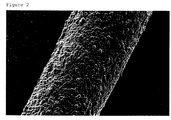
- the wires had a surface roughness R a of 0.3 ⁇ m, see fig 1 and table 1 variant a, here designated variant A.
- the same type of net as used for variant A was coated with an approximately 50 ⁇ m thick spray-coating of Mo onto the Mo-net prior to first time use.
- the net was thereafter pre-coated with a CVD and MTCVD coating of Ti(C,N)+Al 2 O 3 +TiN of a total thickness of 5 ⁇ m.
- the surface roughness, R a was 11 ⁇ m, see fig 2 and table 1 variant c, here designated variant B.
- Cemented carbide inserts of style XOMX0908-ME06 with a composition of 91 wt% WC - 9 wt% Co were used. Before deposition the uncoated substrates were cleaned. A CVD production-coating of Ti(C,N)+TiC+TiN with an approximately 5 ⁇ m total coating thickness was deposited on the inserts. Totally ten nets per variant were used and onto each of the woven Mo-nets 330 inserts were positioned. After production-coating 5% of randomly picked inserts from each net were checked for contact marks. If the marks were of protruding type, the maximum height of the protrusions was measured with an optical Nikon device. If more than one protruding mark on one insert were found the maximum height was taken as the measure of the actual insert. Depending on the height of the protruding mark the inserts were classified into four different classes;
- variant B has much less and smaller marks.
- Variant C Variant D Mean ( ⁇ m) 17 8 Standard deviation ( ⁇ m) 9 3 Minimum ( ⁇ m) 5 0 Maximum ( ⁇ m) 52 17 Class 1 (%) 0.0 0.9 Class 2 (%) 24.4 78.9 Class 3 (%) 47.9 20.2 Class 4 (%) 27.7 0
- the variant C which is according to prior art, works somewhat better than in example 1 but still 28% are not approved. By using the present invention all inserts are approved.
- Variant E Variant F Mean ( ⁇ m) 17 9 Standard deviation ( ⁇ m) 4 3 Minimum ( ⁇ m) 6 0 Maximum ( ⁇ m) 30 17 Class 1 (%) 0.0 1.9 Class 2 (%) 6.9 65.0 Class 3 (%) 75.6 33.1 Class 4 (%), Not approved 17.5 0.0 It can clearly be seen that the spray-coated variant F has much less and smaller marks. Also in this example by using the present invention all inserts are approved, while using prior art 18% are not approved.
Landscapes
- Chemical & Material Sciences (AREA)
- Engineering & Computer Science (AREA)
- Chemical Kinetics & Catalysis (AREA)
- Materials Engineering (AREA)
- Mechanical Engineering (AREA)
- Metallurgy (AREA)
- Organic Chemistry (AREA)
- Physics & Mathematics (AREA)
- Plasma & Fusion (AREA)
- General Chemical & Material Sciences (AREA)
- Chemical Vapour Deposition (AREA)
- Cutting Tools, Boring Holders, And Turrets (AREA)
Applications Claiming Priority (2)
| Application Number | Priority Date | Filing Date | Title |
|---|---|---|---|
| SE0302056 | 2003-07-10 | ||
| SE0302056A SE527351C2 (sv) | 2003-07-10 | 2003-07-10 | Metod att belägga skär |
Publications (2)
| Publication Number | Publication Date |
|---|---|
| EP1496137A1 true EP1496137A1 (de) | 2005-01-12 |
| EP1496137B1 EP1496137B1 (de) | 2006-02-15 |
Family
ID=27764978
Family Applications (1)
| Application Number | Title | Priority Date | Filing Date |
|---|---|---|---|
| EP20040445074 Expired - Lifetime EP1496137B1 (de) | 2003-07-10 | 2004-06-28 | Verfahren zur rationalen, grossvolumigen chemischen Dampfphasenbeschichtung |
Country Status (5)
| Country | Link |
|---|---|
| US (2) | US20050032444A1 (de) |
| EP (1) | EP1496137B1 (de) |
| AT (1) | ATE317920T1 (de) |
| DE (1) | DE602004000402T2 (de) |
| SE (1) | SE527351C2 (de) |
Families Citing this family (2)
| Publication number | Priority date | Publication date | Assignee | Title |
|---|---|---|---|---|
| US7874770B2 (en) † | 2005-03-30 | 2011-01-25 | Sumitomo Electric Hardmetal Corp. | Indexable insert |
| WO2007103578A1 (en) * | 2006-03-09 | 2007-09-13 | Cabot Microelectronics Corporation | Method of polishing a tungsten carbide surface |
Citations (2)
| Publication number | Priority date | Publication date | Assignee | Title |
|---|---|---|---|---|
| US4619866A (en) * | 1980-07-28 | 1986-10-28 | Santrade Limited | Method of making a coated cemented carbide body and resulting body |
| EP0424620A2 (de) * | 1989-09-22 | 1991-05-02 | Balzers Aktiengesellschaft | Verfahren und Anlage zum chemischen Beschichten von einander gegenüberliegenden Oberflächenbereichen eines Werkstückes |
Family Cites Families (12)
| Publication number | Priority date | Publication date | Assignee | Title |
|---|---|---|---|---|
| DE3902532C1 (de) | 1989-01-28 | 1989-11-23 | Krupp Widia Gmbh, 4300 Essen, De | |
| SE9101953D0 (sv) * | 1991-06-25 | 1991-06-25 | Sandvik Ab | A1203 coated sintered body |
| JP2519632B2 (ja) * | 1992-06-26 | 1996-07-31 | 東京タングステン株式会社 | モリブデン又はモリブデン基合金網及びその製造方法 |
| JP3563789B2 (ja) * | 1993-12-22 | 2004-09-08 | キヤノン株式会社 | 電子写真感光体の製造方法及び該製造方法に用いられる治具 |
| SE509984C2 (sv) * | 1994-03-18 | 1999-03-29 | Sandvik Ab | Chargeringssystem för CVD |
| US20020041928A1 (en) * | 1997-03-26 | 2002-04-11 | Leonid V. Budaragin | Method for coating substrate with metal oxide coating |
| US6544599B1 (en) * | 1996-07-31 | 2003-04-08 | Univ Arkansas | Process and apparatus for applying charged particles to a substrate, process for forming a layer on a substrate, products made therefrom |
| US6494937B1 (en) * | 2001-09-27 | 2002-12-17 | Idatech, Llc | Hydrogen purification devices, components and fuel processing systems containing the same |
| JP4236292B2 (ja) * | 1997-03-06 | 2009-03-11 | 日本碍子株式会社 | ウエハー吸着装置およびその製造方法 |
| US6231969B1 (en) * | 1997-08-11 | 2001-05-15 | Drexel University | Corrosion, oxidation and/or wear-resistant coatings |
| EP1323847A3 (de) * | 2001-12-28 | 2005-09-14 | Seco Tools Ab | Beschichteter Hartmetallkörper und Verfahren zu seiner Herstellung |
| CZ2006399A3 (cs) * | 2003-12-22 | 2006-09-13 | Seco Tools Ab | Nosic a zpusob pokrývání rezacích nástroju |
-
2003
- 2003-07-10 SE SE0302056A patent/SE527351C2/sv not_active IP Right Cessation
-
2004
- 2004-06-28 AT AT04445074T patent/ATE317920T1/de active
- 2004-06-28 EP EP20040445074 patent/EP1496137B1/de not_active Expired - Lifetime
- 2004-06-28 DE DE200460000402 patent/DE602004000402T2/de not_active Expired - Lifetime
- 2004-07-01 US US10/880,447 patent/US20050032444A1/en not_active Abandoned
-
2006
- 2006-12-05 US US11/633,476 patent/US7740909B2/en not_active Expired - Fee Related
Patent Citations (2)
| Publication number | Priority date | Publication date | Assignee | Title |
|---|---|---|---|---|
| US4619866A (en) * | 1980-07-28 | 1986-10-28 | Santrade Limited | Method of making a coated cemented carbide body and resulting body |
| EP0424620A2 (de) * | 1989-09-22 | 1991-05-02 | Balzers Aktiengesellschaft | Verfahren und Anlage zum chemischen Beschichten von einander gegenüberliegenden Oberflächenbereichen eines Werkstückes |
Also Published As
| Publication number | Publication date |
|---|---|
| DE602004000402T2 (de) | 2006-11-09 |
| DE602004000402D1 (de) | 2006-04-20 |
| ATE317920T1 (de) | 2006-03-15 |
| US20070111618A1 (en) | 2007-05-17 |
| SE0302056L (sv) | 2005-01-25 |
| EP1496137B1 (de) | 2006-02-15 |
| SE0302056D0 (sv) | 2003-07-10 |
| SE527351C2 (sv) | 2006-02-14 |
| US7740909B2 (en) | 2010-06-22 |
| US20050032444A1 (en) | 2005-02-10 |
Similar Documents
| Publication | Publication Date | Title |
|---|---|---|
| KR20060123381A (ko) | 절삭 공구를 코팅하기 위한 캐리어체 및 절삭 공구 코팅방법 | |
| US10286453B2 (en) | Alumina coated cutting tool | |
| US7544024B2 (en) | Coated cutting insert and manufacturing method thereof | |
| KR101167343B1 (ko) | 날끝 교환형 절삭팁 및 그 제조 방법 | |
| CN1854335B (zh) | 涂层刀具刀片 | |
| KR102910121B1 (ko) | 코팅된 절삭 공구 | |
| KR101307125B1 (ko) | 날끝 교환형 절삭 팁 및 그 제조 방법 | |
| CN109312474A (zh) | Cvd涂层切削工具 | |
| WO2014060414A1 (en) | Coated cutting tool with patterned surface area | |
| KR20060132507A (ko) | 코팅된 절삭 공구 인서트 | |
| KR20110083633A (ko) | 코팅된 공구 및 코팅된 공구의 제조 방법 | |
| US7553113B2 (en) | Indexable insert and method of manufacturing the same | |
| JP6697696B2 (ja) | 被覆切削工具 | |
| KR101455142B1 (ko) | 내식성이 우수한 피복 물품의 제조 방법 및 피복 물품 | |
| SE528012C2 (sv) | Belagt hårdmetallskär med skarp skäregg avsett för metallbearbetning samt sätt för dess framställning | |
| EP1496137B1 (de) | Verfahren zur rationalen, grossvolumigen chemischen Dampfphasenbeschichtung | |
| KR20110078462A (ko) | 절삭공구의 제조방법 및 상기 방법으로 제조된 절삭공구 | |
| SE526833C2 (sv) | Bärarkropp och metod för att belägga verktygsskär |
Legal Events
| Date | Code | Title | Description |
|---|---|---|---|
| PUAI | Public reference made under article 153(3) epc to a published international application that has entered the european phase |
Free format text: ORIGINAL CODE: 0009012 |
|
| AK | Designated contracting states |
Kind code of ref document: A1 Designated state(s): AT BE BG CH CY CZ DE DK EE ES FI FR GB GR HU IE IT LI LU MC NL PL PT RO SE SI SK TR |
|
| AX | Request for extension of the european patent |
Extension state: AL HR LT LV MK |
|
| GRAP | Despatch of communication of intention to grant a patent |
Free format text: ORIGINAL CODE: EPIDOSNIGR1 |
|
| 17P | Request for examination filed |
Effective date: 20050611 |
|
| AKX | Designation fees paid |
Designated state(s): AT BE BG CH CY CZ DE DK EE ES FI FR GB GR HU IE IT LI LU MC NL PL PT RO SE SI SK TR |
|
| GRAS | Grant fee paid |
Free format text: ORIGINAL CODE: EPIDOSNIGR3 |
|
| GRAA | (expected) grant |
Free format text: ORIGINAL CODE: 0009210 |
|
| RIN1 | Information on inventor provided before grant (corrected) |
Inventor name: LAITILA, EDWARD Inventor name: DANIELSEN, BO Inventor name: LIFVERGREN, BJOERN Inventor name: PETTERSSON, LENA Inventor name: BERGSTEDT, JOHNNY |
|
| AK | Designated contracting states |
Kind code of ref document: B1 Designated state(s): AT BE BG CH CY CZ DE DK EE ES FI FR GB GR HU IE IT LI LU MC NL PL PT RO SE SI SK TR |
|
| PG25 | Lapsed in a contracting state [announced via postgrant information from national office to epo] |
Ref country code: IT Free format text: LAPSE BECAUSE OF FAILURE TO SUBMIT A TRANSLATION OF THE DESCRIPTION OR TO PAY THE FEE WITHIN THE PRESCRIBED TIME-LIMIT;WARNING: LAPSES OF ITALIAN PATENTS WITH EFFECTIVE DATE BEFORE 2007 MAY HAVE OCCURRED AT ANY TIME BEFORE 2007. THE CORRECT EFFECTIVE DATE MAY BE DIFFERENT FROM THE ONE RECORDED. Effective date: 20060215 Ref country code: BE Free format text: LAPSE BECAUSE OF FAILURE TO SUBMIT A TRANSLATION OF THE DESCRIPTION OR TO PAY THE FEE WITHIN THE PRESCRIBED TIME-LIMIT Effective date: 20060215 Ref country code: NL Free format text: LAPSE BECAUSE OF FAILURE TO SUBMIT A TRANSLATION OF THE DESCRIPTION OR TO PAY THE FEE WITHIN THE PRESCRIBED TIME-LIMIT Effective date: 20060215 Ref country code: FI Free format text: LAPSE BECAUSE OF FAILURE TO SUBMIT A TRANSLATION OF THE DESCRIPTION OR TO PAY THE FEE WITHIN THE PRESCRIBED TIME-LIMIT Effective date: 20060215 Ref country code: SI Free format text: LAPSE BECAUSE OF FAILURE TO SUBMIT A TRANSLATION OF THE DESCRIPTION OR TO PAY THE FEE WITHIN THE PRESCRIBED TIME-LIMIT Effective date: 20060215 Ref country code: SK Free format text: LAPSE BECAUSE OF FAILURE TO SUBMIT A TRANSLATION OF THE DESCRIPTION OR TO PAY THE FEE WITHIN THE PRESCRIBED TIME-LIMIT Effective date: 20060215 Ref country code: PL Free format text: LAPSE BECAUSE OF FAILURE TO SUBMIT A TRANSLATION OF THE DESCRIPTION OR TO PAY THE FEE WITHIN THE PRESCRIBED TIME-LIMIT Effective date: 20060215 Ref country code: RO Free format text: LAPSE BECAUSE OF FAILURE TO SUBMIT A TRANSLATION OF THE DESCRIPTION OR TO PAY THE FEE WITHIN THE PRESCRIBED TIME-LIMIT Effective date: 20060215 |
|
| REG | Reference to a national code |
Ref country code: GB Ref legal event code: FG4D Ref country code: CH Ref legal event code: EP |
|
| REG | Reference to a national code |
Ref country code: IE Ref legal event code: FG4D |
|
| REG | Reference to a national code |
Ref country code: SE Ref legal event code: TRGR |
|
| REF | Corresponds to: |
Ref document number: 602004000402 Country of ref document: DE Date of ref document: 20060420 Kind code of ref document: P |
|
| PG25 | Lapsed in a contracting state [announced via postgrant information from national office to epo] |
Ref country code: BG Free format text: LAPSE BECAUSE OF FAILURE TO SUBMIT A TRANSLATION OF THE DESCRIPTION OR TO PAY THE FEE WITHIN THE PRESCRIBED TIME-LIMIT Effective date: 20060515 Ref country code: DK Free format text: LAPSE BECAUSE OF FAILURE TO SUBMIT A TRANSLATION OF THE DESCRIPTION OR TO PAY THE FEE WITHIN THE PRESCRIBED TIME-LIMIT Effective date: 20060515 |
|
| PG25 | Lapsed in a contracting state [announced via postgrant information from national office to epo] |
Ref country code: ES Free format text: LAPSE BECAUSE OF FAILURE TO SUBMIT A TRANSLATION OF THE DESCRIPTION OR TO PAY THE FEE WITHIN THE PRESCRIBED TIME-LIMIT Effective date: 20060526 |
|
| REG | Reference to a national code |
Ref country code: CH Ref legal event code: NV Representative=s name: BOVARD AG PATENTANWAELTE |
|
| PG25 | Lapsed in a contracting state [announced via postgrant information from national office to epo] |
Ref country code: IE Free format text: LAPSE BECAUSE OF NON-PAYMENT OF DUE FEES Effective date: 20060628 |
|
| PG25 | Lapsed in a contracting state [announced via postgrant information from national office to epo] |
Ref country code: MC Free format text: LAPSE BECAUSE OF NON-PAYMENT OF DUE FEES Effective date: 20060630 |
|
| PG25 | Lapsed in a contracting state [announced via postgrant information from national office to epo] |
Ref country code: PT Free format text: LAPSE BECAUSE OF FAILURE TO SUBMIT A TRANSLATION OF THE DESCRIPTION OR TO PAY THE FEE WITHIN THE PRESCRIBED TIME-LIMIT Effective date: 20060717 |
|
| NLV1 | Nl: lapsed or annulled due to failure to fulfill the requirements of art. 29p and 29m of the patents act | ||
| PLBE | No opposition filed within time limit |
Free format text: ORIGINAL CODE: 0009261 |
|
| STAA | Information on the status of an ep patent application or granted ep patent |
Free format text: STATUS: NO OPPOSITION FILED WITHIN TIME LIMIT |
|
| 26N | No opposition filed |
Effective date: 20061116 |
|
| EN | Fr: translation not filed | ||
| PG25 | Lapsed in a contracting state [announced via postgrant information from national office to epo] |
Ref country code: FR Free format text: LAPSE BECAUSE OF FAILURE TO SUBMIT A TRANSLATION OF THE DESCRIPTION OR TO PAY THE FEE WITHIN THE PRESCRIBED TIME-LIMIT Effective date: 20070105 |
|
| PG25 | Lapsed in a contracting state [announced via postgrant information from national office to epo] |
Ref country code: CZ Free format text: LAPSE BECAUSE OF FAILURE TO SUBMIT A TRANSLATION OF THE DESCRIPTION OR TO PAY THE FEE WITHIN THE PRESCRIBED TIME-LIMIT Effective date: 20060215 Ref country code: GR Free format text: LAPSE BECAUSE OF FAILURE TO SUBMIT A TRANSLATION OF THE DESCRIPTION OR TO PAY THE FEE WITHIN THE PRESCRIBED TIME-LIMIT Effective date: 20060516 |
|
| PG25 | Lapsed in a contracting state [announced via postgrant information from national office to epo] |
Ref country code: EE Free format text: LAPSE BECAUSE OF FAILURE TO SUBMIT A TRANSLATION OF THE DESCRIPTION OR TO PAY THE FEE WITHIN THE PRESCRIBED TIME-LIMIT Effective date: 20060215 |
|
| PG25 | Lapsed in a contracting state [announced via postgrant information from national office to epo] |
Ref country code: TR Free format text: LAPSE BECAUSE OF FAILURE TO SUBMIT A TRANSLATION OF THE DESCRIPTION OR TO PAY THE FEE WITHIN THE PRESCRIBED TIME-LIMIT Effective date: 20060215 Ref country code: LU Free format text: LAPSE BECAUSE OF NON-PAYMENT OF DUE FEES Effective date: 20060628 Ref country code: HU Free format text: LAPSE BECAUSE OF FAILURE TO SUBMIT A TRANSLATION OF THE DESCRIPTION OR TO PAY THE FEE WITHIN THE PRESCRIBED TIME-LIMIT Effective date: 20060816 |
|
| PG25 | Lapsed in a contracting state [announced via postgrant information from national office to epo] |
Ref country code: FR Free format text: LAPSE BECAUSE OF FAILURE TO SUBMIT A TRANSLATION OF THE DESCRIPTION OR TO PAY THE FEE WITHIN THE PRESCRIBED TIME-LIMIT Effective date: 20060215 Ref country code: CY Free format text: LAPSE BECAUSE OF FAILURE TO SUBMIT A TRANSLATION OF THE DESCRIPTION OR TO PAY THE FEE WITHIN THE PRESCRIBED TIME-LIMIT Effective date: 20060215 |
|
| REG | Reference to a national code |
Ref country code: CH Ref legal event code: PFA Owner name: SECO TOOLS AB Free format text: SECO TOOLS AB# #S-737 82 FAGERSTA (SE) -TRANSFER TO- SECO TOOLS AB# #S-737 82 FAGERSTA (SE) |
|
| PGFP | Annual fee paid to national office [announced via postgrant information from national office to epo] |
Ref country code: DE Payment date: 20120620 Year of fee payment: 9 Ref country code: CH Payment date: 20120612 Year of fee payment: 9 |
|
| PGFP | Annual fee paid to national office [announced via postgrant information from national office to epo] |
Ref country code: GB Payment date: 20120627 Year of fee payment: 9 Ref country code: SE Payment date: 20120612 Year of fee payment: 9 |
|
| PGFP | Annual fee paid to national office [announced via postgrant information from national office to epo] |
Ref country code: AT Payment date: 20120529 Year of fee payment: 9 |
|
| PG25 | Lapsed in a contracting state [announced via postgrant information from national office to epo] |
Ref country code: SE Free format text: LAPSE BECAUSE OF NON-PAYMENT OF DUE FEES Effective date: 20130629 |
|
| REG | Reference to a national code |
Ref country code: CH Ref legal event code: PL |
|
| REG | Reference to a national code |
Ref country code: SE Ref legal event code: EUG |
|
| REG | Reference to a national code |
Ref country code: AT Ref legal event code: MM01 Ref document number: 317920 Country of ref document: AT Kind code of ref document: T Effective date: 20130628 |
|
| GBPC | Gb: european patent ceased through non-payment of renewal fee |
Effective date: 20130628 |
|
| REG | Reference to a national code |
Ref country code: DE Ref legal event code: R119 Ref document number: 602004000402 Country of ref document: DE Effective date: 20140101 |
|
| PG25 | Lapsed in a contracting state [announced via postgrant information from national office to epo] |
Ref country code: DE Free format text: LAPSE BECAUSE OF NON-PAYMENT OF DUE FEES Effective date: 20140101 Ref country code: GB Free format text: LAPSE BECAUSE OF NON-PAYMENT OF DUE FEES Effective date: 20130628 Ref country code: LI Free format text: LAPSE BECAUSE OF NON-PAYMENT OF DUE FEES Effective date: 20130630 Ref country code: CH Free format text: LAPSE BECAUSE OF NON-PAYMENT OF DUE FEES Effective date: 20130630 |
|
| PG25 | Lapsed in a contracting state [announced via postgrant information from national office to epo] |
Ref country code: AT Free format text: LAPSE BECAUSE OF NON-PAYMENT OF DUE FEES Effective date: 20130628 |