EP1496437A1 - Appareil de stockage de donnees - Google Patents
Appareil de stockage de donnees Download PDFInfo
- Publication number
- EP1496437A1 EP1496437A1 EP03746481A EP03746481A EP1496437A1 EP 1496437 A1 EP1496437 A1 EP 1496437A1 EP 03746481 A EP03746481 A EP 03746481A EP 03746481 A EP03746481 A EP 03746481A EP 1496437 A1 EP1496437 A1 EP 1496437A1
- Authority
- EP
- European Patent Office
- Prior art keywords
- data
- recorded
- host device
- sector
- block
- Prior art date
- Legal status (The legal status is an assumption and is not a legal conclusion. Google has not performed a legal analysis and makes no representation as to the accuracy of the status listed.)
- Ceased
Links
Images


Classifications
-
- G—PHYSICS
- G06—COMPUTING OR CALCULATING; COUNTING
- G06F—ELECTRIC DIGITAL DATA PROCESSING
- G06F12/00—Accessing, addressing or allocating within memory systems or architectures
-
- G—PHYSICS
- G07—CHECKING-DEVICES
- G07F—COIN-FREED OR LIKE APPARATUS
- G07F7/00—Mechanisms actuated by objects other than coins to free or to actuate vending, hiring, coin or paper currency dispensing or refunding apparatus
- G07F7/08—Mechanisms actuated by objects other than coins to free or to actuate vending, hiring, coin or paper currency dispensing or refunding apparatus by coded identity card or credit card or other personal identification means
- G07F7/10—Mechanisms actuated by objects other than coins to free or to actuate vending, hiring, coin or paper currency dispensing or refunding apparatus by coded identity card or credit card or other personal identification means together with a coded signal, e.g. in the form of personal identification information, like personal identification number [PIN] or biometric data
- G07F7/1008—Active credit-cards provided with means to personalise their use, e.g. with PIN-introduction/comparison system
-
- G—PHYSICS
- G06—COMPUTING OR CALCULATING; COUNTING
- G06F—ELECTRIC DIGITAL DATA PROCESSING
- G06F3/00—Input arrangements for transferring data to be processed into a form capable of being handled by the computer; Output arrangements for transferring data from processing unit to output unit, e.g. interface arrangements
- G06F3/06—Digital input from, or digital output to, record carriers, e.g. RAID, emulated record carriers or networked record carriers
- G06F3/0601—Interfaces specially adapted for storage systems
- G06F3/0602—Interfaces specially adapted for storage systems specifically adapted to achieve a particular effect
- G06F3/0604—Improving or facilitating administration, e.g. storage management
- G06F3/0607—Improving or facilitating administration, e.g. storage management by facilitating the process of upgrading existing storage systems, e.g. for improving compatibility between host and storage device
-
- G—PHYSICS
- G06—COMPUTING OR CALCULATING; COUNTING
- G06F—ELECTRIC DIGITAL DATA PROCESSING
- G06F3/00—Input arrangements for transferring data to be processed into a form capable of being handled by the computer; Output arrangements for transferring data from processing unit to output unit, e.g. interface arrangements
- G06F3/06—Digital input from, or digital output to, record carriers, e.g. RAID, emulated record carriers or networked record carriers
- G06F3/0601—Interfaces specially adapted for storage systems
- G06F3/0628—Interfaces specially adapted for storage systems making use of a particular technique
- G06F3/0638—Organizing or formatting or addressing of data
- G06F3/064—Management of blocks
-
- G—PHYSICS
- G06—COMPUTING OR CALCULATING; COUNTING
- G06F—ELECTRIC DIGITAL DATA PROCESSING
- G06F3/00—Input arrangements for transferring data to be processed into a form capable of being handled by the computer; Output arrangements for transferring data from processing unit to output unit, e.g. interface arrangements
- G06F3/06—Digital input from, or digital output to, record carriers, e.g. RAID, emulated record carriers or networked record carriers
- G06F3/0601—Interfaces specially adapted for storage systems
- G06F3/0628—Interfaces specially adapted for storage systems making use of a particular technique
- G06F3/0638—Organizing or formatting or addressing of data
- G06F3/0643—Management of files
-
- G—PHYSICS
- G06—COMPUTING OR CALCULATING; COUNTING
- G06F—ELECTRIC DIGITAL DATA PROCESSING
- G06F3/00—Input arrangements for transferring data to be processed into a form capable of being handled by the computer; Output arrangements for transferring data from processing unit to output unit, e.g. interface arrangements
- G06F3/06—Digital input from, or digital output to, record carriers, e.g. RAID, emulated record carriers or networked record carriers
- G06F3/0601—Interfaces specially adapted for storage systems
- G06F3/0668—Interfaces specially adapted for storage systems adopting a particular infrastructure
- G06F3/0671—In-line storage system
- G06F3/0673—Single storage device
- G06F3/0679—Non-volatile semiconductor memory device, e.g. flash memory, one time programmable memory [OTP]
-
- G—PHYSICS
- G06—COMPUTING OR CALCULATING; COUNTING
- G06F—ELECTRIC DIGITAL DATA PROCESSING
- G06F3/00—Input arrangements for transferring data to be processed into a form capable of being handled by the computer; Output arrangements for transferring data from processing unit to output unit, e.g. interface arrangements
- G06F3/06—Digital input from, or digital output to, record carriers, e.g. RAID, emulated record carriers or networked record carriers
- G06F3/08—Digital input from, or digital output to, record carriers, e.g. RAID, emulated record carriers or networked record carriers from or to individual record carriers, e.g. punched card, memory card, integrated circuit [IC] card or smart card
-
- G—PHYSICS
- G06—COMPUTING OR CALCULATING; COUNTING
- G06Q—INFORMATION AND COMMUNICATION TECHNOLOGY [ICT] SPECIALLY ADAPTED FOR ADMINISTRATIVE, COMMERCIAL, FINANCIAL, MANAGERIAL OR SUPERVISORY PURPOSES; SYSTEMS OR METHODS SPECIALLY ADAPTED FOR ADMINISTRATIVE, COMMERCIAL, FINANCIAL, MANAGERIAL OR SUPERVISORY PURPOSES, NOT OTHERWISE PROVIDED FOR
- G06Q20/00—Payment architectures, schemes or protocols
- G06Q20/30—Payment architectures, schemes or protocols characterised by the use of specific devices or networks
- G06Q20/34—Payment architectures, schemes or protocols characterised by the use of specific devices or networks using cards, e.g. integrated circuit [IC] cards or magnetic cards
- G06Q20/346—Cards serving only as information carrier of service
Definitions
- This invention relates to a data storage device having an inner non-volatile semiconductor memory.
- an IC memory device termed a memory card
- This IC memory device is used so as to be mounted to or dismounted from the recording and/or reproducing apparatus.
- the memory card is able to store a large variety of digital data, such as still image data, moving picture data, speech data or music data. For this reason, the memory card is used as an external storage medium in a wide variety of host devices, such as a portable information terminal, a desk top computer, a notebook computer, a mobile phone, an audio device or a household electrical device.
- the host device employing the memory card as an external storage medium, is sometimes provided with an internal storage medium, such as a hard disc.
- the hard disc is usually accessed with a logical format from the host device, using a file system, called the MS-DOS (trademark), as a vehicle.
- the MS-DOS trademark
- the common file system including the MS-DOS, is desirably applicable to the memory card.
- the MBR master boot record
- PBR partition boot record
- FAT file allocation table
- the root entry record as file management data
- the storage medium may be accessed by an operating system on the side of the host device. Consequently, the memory card also is initialized by the host device writing the aforementioned file management data in its flash memory.
- a flash memory of a memory card differs from that of another memory card of the same standard as the first-stated memory card. If the memory cards of different capacities are to be initialized as external mediums, a host device, operating as a data recording and/or reproducing apparatus, has to be provided with initialization parameters or with initialization controlling processing programs, representing the contents of the MBR and so forth associated with the respective different capacities.
- the host device cannot cope with a memory card of a new capacity, even if the host device is provided with initialization parameters.
- the present invention provides a removable data storage device, detachably mounted to a host device, comprising a non-volatile semiconductor memory in which data recorded thereon is erased batch-wise in terms of a block of a predetermined data volume as a unit, a system information storage unit having the inner information of the data storage device recorded therein, an interface for inputting/outputting data between the data storage device and the host device, and a controller for managing control for the semiconductor memory, based on a command supplied from the host device over the interface.
- a user area as an area where data is recorded by a user, is provided in the semiconductor memory and file management data is recorded in the user area, in agreement with the logical format, executing file management in terms of a cluster of a size equal to 1/n times the size of the block, as a unit, n being an integer not less than two, the host device accessing the user area based on the logical format.
- the controller When supplied with an initialization command from the host device, the controller records in the semiconductor memory the file management data which is in agreement with parameters stored in the system information storage unit.
- a small-sized IC memory device is termed a memory card
- a data processing apparatus to which the memory card is connected, is termed a host device.
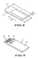
- a memory card 1 of the present invention includes an inner non-volatile semiconductor memory (IC memory), and is able to store various digital data, such as still picture data, moving picture data, speech data and music data.
- This memory card 1 operates as an external storage medium for a host device 2, such as, for example a portable information terminal, a desk top computer, a notebook computer, a mobile phone, audio equipment or a household electrical apparatus.
- the memory card 1 is used in such a state in which it is inserted into an insertion/removal port 3 provided to the host device 2.
- the memory card 1 can be freely inserted into and detached from the insertion/removal port 3 by a user.
- the memory card 1 inserted into a host device can be extracted therefrom and inserted into another host device. That is, the present memory card 1 can be used for exchanging data between the different host devices.
- the memory card 1 and the host device 2 transfer data over a parallel interface employing a six line half duplex parallel protocol configured for transmitting six signals, namely 4-bit parallel data, a clock signal and a bus state signal.
- the memory card 1 of the present invention is formed as a substantially rectangular thin sheet, having a length L 1 along the longitudinal direction of 50 mm, a width W 1 of 21.45 mm and a thickness D 1 of 2.8 mm.
- the memory card 1 has its one surface as a front surface 1a and its opposite surface as a reverse surface 1b.
- On the reverse surface 1b towards one longitudinal end of the memory card 1 are formed a set of connection terminals 4 as ten planar electrodes, as shown in Fig.3. These electrodes, forming the set of the connection terminals 4, are provided parallel to one another along the width of the memory card 1. Between the neighboring electrodes, there are provided partitions 5 upstanding from the reverse surface 1b.
- partitions 5 serve for preventing the connection terminals, connected to the respective electrodes, from being contacted with the other electrodes.
- a slide switch 6 for prohibiting inadvertent erasure is provided centrally towards the aforementioned one end of the reverse surface 1b of the memory card 1, as shown in Fig.3.
- the host device 2 to which is mounted the memory card 1 is provided with the insertion/removal port 3 for inserting and detaching the memory card 1.
- This insertion/removal port 3 is formed in the front surface of the host device 2 as an opening of the same width W 1 and thickness D 1 as those of the memory card 1, as shown in Fig.1.
- the memory card 1, inserted into the host device 2 through the insertion/removal port 3, is held by the host device 2 against incidental detachment by the connection terminals of the host device 2 being connected to the respective electrodes that make up the set of the connection terminals 4.
- the connection terminals, not shown, provided to the host device 2 are provided with ten contacts in meeting with the number of the electrodes that make up the set of the connection terminals 4 provided to the loaded memory card 1.
- the memory card 1 according to the present invention is loaded on the host device 2, with its end provided with the set of the connection terminals 4 as an inserting end and with the direction of an arrow X 1 in Fig.2 as an inserting direction.
- the respective electrodes that make up the set of the connection terminals 4 are connected to the respective contacts of the connection terminals provided to the host device 2 to enable exchange of electrical signals.
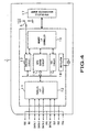
- the memory card 1 of the present invention includes a parallel interfacing (I/F) circuit 12, a register circuit 13, a data buffer circuit 14, an ECC circuit 15, a memory I/F controller 16, a non-volatile semiconductor memory 17, and an oscillation controlling circuit 18, as shown in Fig.4.
- I/F parallel interfacing
- the parallel I/F circuit 12 is a circuit for transmitting data with the host device 2 using the six-line half duplex parallel type data transfer protocol.
- the register circuit 13 is a circuit for storage of operation controlling commands for the memory I/F controller 16, transferred from the host equipment, the inner states of the memory card 1, various parameters needed in executing the controlling commands, or the file management information in the non-volatile semiconductor memory 17.
- the operation controlling commands are referred to below as control commands.
- This register circuit 13 is accessed from both the host device 2 and the memory I/F controller 16. Meanwhile, the host device 2 accesses the register circuit 13, using a transfer protocol command TPC as provided for on the data transfer protocol of the present memory card. That is, this TPC is used in case the host device 2 writes or reads out the control command or various parameters stored in the register circuit 13.
- the data buffer circuit 14 is a memory circuit for transient storage of data written in the non-volatile semiconductor memory 17 and data read out from the non-volatile semiconductor memory 17. That is, when data is written from the host device 2 to the non-volatile semiconductor memory 17, data as a subject of writing is transferred from the host device 2 to the data buffer circuit 14 in accordance with the data transfer protocol and subsequently the data as a subject of writing, stored in the data buffer circuit 14, is written by the memory I/F controller 16 in the non-volatile semiconductor memory 17.
- the memory I/F controller 16 When the data is read out from the non-volatile semiconductor memory 17 to the host device 2, the memory I/F controller 16 reads out data as a subject of readout from the non-volatile semiconductor memory 17 to store the read-out data transiently in the data buffer circuit 14. The data as a subject of readout is then transferred from the data buffer circuit 14 to the host device 2 in accordance with the data transfer protocol.
- the data buffer circuit 14 has a data capacity corresponding to a preset data write unit, such as, for example, the data capacity of 512 bytes, which is the same as the page size of the flash memory.
- the host device 2 accesses the data buffer circuit 14 using the TPC. That is, if the host device 2 writes or reads out the data stored in the data buffer circuit 14, the TPC is used.
- the ECC circuit 15 appends the error correction code (ECC) to data to be written in the non-volatile semiconductor memory 17.
- ECC error correction code
- the ECC circuit 15 performs error correction coding on the read out data based on the error correction code appended to the data read out from the non-volatile semiconductor memory 17. For example, 3 bytes of the error correction code are appended to a data unit of 512 bytes.
- the memory I/F controller 16 performs control, in accordance with control commands stored in the register circuit 13, for exchanging data between the data buffer circuit 14 and the non-volatile semiconductor memory 17, supervising data security of the non-volatile semiconductor memory 17, managing the other functions of the memory card 1, and for updating the data stored in the register circuit 13.
- the non-volatile semiconductor memory 17 is e.g. a non-volatile semiconductor memory, such as a NAND type flash memory.
- the capacity of the non-volatile semiconductor memory 17 is e.g.16 Mbytes, 32 Mbytes, 64 Mbytes or 128 Mbytes.
- the erasure block unit of the non-volatile semiconductor memory 17 is e.g. 16 Kbytes.
- the read/write unit is also termed a page and is 512 bytes as is that of the data buffer circuit 14.
- the oscillation controlling circuit 18 generates operating clocks in the present memory card 1.
- connection terminals of the memory card 1 there are provided VSS, VCC, DATA0, DATA1, DATA2, DATA3, BS, CLK and INS terminals. Since two terminals are provided as the VSS terminals, a total of ten connection terminals are provided in the memory card 1. Similar connection terminals are provided on the side of the host device 2.
- VSS reference 0 voltage
- VCC power supply voltage
- the data signal (DATA0) of the lowermost bit of the 4-bit parallel data, transferred between the memory card 1 and the host device 2, is supplied to or output from the DATA0 terminal.
- the data signal (DATA1) of the second lower bit of the 4-bit parallel data, transferred between the memory card 1 and the host device 2, is supplied to or output from the DATA1 terminal.
- the data signal (DATA2) of the third lower bit of the 4-bit parallel data, transferred between the memory card 1 and the host device 2, is supplied to or output from the DATA2 terminal.
- the data signal (DATA3) of the fourth lower bit of the 4-bit parallel data, transferred between the memory card 1 and the host device 2 is supplied to or output from the DATA3 terminal.
- a bus state signal is supplied from the host device to the memory card via BS terminal.
- a clock signal is supplied from the host device to the CLK terminal.
- the INS terminal is used for insertion/withdrawal detection for the host device 2 to check whether or not the memory card has been inserted into a slot formed in the host device 2.
- the INS terminal of the host device 2 is connected to a pull-up resistor, not shown.
- the interfacing functions of the host device 2 are made up by a file manager 31, a TPC interface 32, and a parallel interface 33.
- the interfacing functions of the memory card 1 is made up by a parallel interface 33, a register 35, a data buffer 36, a memory controller 37 and a memory 38.
- the file manager 31 is an operation system of the host device and supervises the files stored in the memory card 1 and the files stored in other mediums of the host device.
- the MS-DOS Microsoft Disc Operating System, registered trademark
- the file manager 31 also supervises the other storage mediums connected to the host device 2 by the MS-DOS.
- the file manager 31 is a function implemented within a controller in the host device.
- the TPC interface 32 is an interfacing function as a lower layer in the file manager 31.
- the TPC interface 32 accesses the register 35 and the data buffer 36 in the memory card 1 by the data transfer protocol which has defined the commands peculiar to the present interface (TPC: transfer protocol command).
- This TPC interface 32 is a function implemented by e.g. a controller in the host device 2.
- the parallel interfaces 33, 34 represent lower layers in the TPC interface 32 and proves a physical hierarchical layer of the present interfacing system.
- the parallel interfaces 33, 34 transfer data in accordance with a six line half duplex parallel protocol configured for transmitting six signals, namely 4-bit parallel data, a clock signal and a bus state signal.
- the parallel interfaces 33, 34 represent the functions implemented by the parallel I/F circuit 12.
- the register 35 is designed to store control commands transmitted from the host, the inner state of the memory card, data addresses for accessing the memory 38, various parameters required in executing the memory commands or the file management information in the memory.
- the register 35 is a function implemented on the register circuit 13 of the memory card 1.
- the data buffer 36 is a buffer area for transient storage of data written in the memory 38 or read out from the memory 38.
- the data buffer 36 is a function implemented on the data buffer circuit 14 of the memory card 1.
- the memory I/F controller 37 performs control in executing data readout, data write or data erasure between the data buffer 36 and the memory 38 in accordance with the various information and commands stored in the register 35, or in updating the various information in the register 35.
- the memory I/F controller 37 is a function implemented by the memory I/F controller 16 on the host device 2.
- the memory 38 is a data memory area and is designed as a virtual memory as an intrinsic model through the memory I/F controller 37.
- the memory 38 is a function implemented by the non-volatile semiconductor memory 17 on the memory card 1.
- data stored in other mediums, supervised by the file manager 31, can be transferred to the memory 38 through the parallel interfaces 33, 34. Since the file manager 31 supervises the present memory card and other storage mediums by the operation system (MS-DOS), it is possible to transfer data stored in the memory 38 to the other storage mediums or to transfer data stored in the other storage mediums to the memory 38.
- MS-DOS operation system
- the memory card 1 is made up by a user area and a system area, in which to store e.g. the inner information of the present memory card 1. Both the user area and the system area can be accessed from the host device 2 using the control commands. It should be noted however that the user area and the system area are formed in respective different address spaces and are accessed by the host device 2 using respective different commands.
- the user area is physically split in terms of a block of e.g. 64 Kbytes or 128 Kbytes as a unit.
- This block represents a unit of batch erasure in the present memory card 1. That is, the erasure block in the flash memory corresponds to the present block.
- the effective block is a block where entity data of a file is recorded.
- the spare block is an area in which substitution data for late defects are recorded.
- the user area is recognized from the host device 2 as being an area which is continuous on the sector basis. However, it is internally managed by logical block numbers, derived from sector numbers, recording valid data, and by physical block numbers.
- the information showing the relationship of correspondence between the logical block numbers and the physical block numbers is recorded in a redundant area, as a management area for the physical blocks, while being recorded in a system area that cannot be accessed from the host device 2 in a state the relationship of correspondence is arranged as data.
- each block In each block are set physical block numbers specifying the block storage locations. These physical block numbers are set uniquely without dependency on whether a block in question is an effective block or a spare block. In the effective block are recorded the logical block numbers. These logical block numbers are written in predetermined areas in the respective blocks. The logical block numbers are recorded at the time of initializing the present memory card 1. If malfunctions occur in a block, the logical block number of the malfunctioning block is written in the unrecorded spare block by way of substitution of the logical block number.
- Each block is split in terms of a write/readout unit, termed a page, as a unit. This page is in one-for-one correspondence to the sector in the logical format as later explained.
- the logical block number accorded to each block is uniquely associated with the cluster number and the LBA sector number in the logical format as later explained.
- the data storage area is virtually accessed from the side of the host device 2 with the logical format as later explained.
- the memory I/F controller 16 effects address conversion using a logical/physical conversion table stating the relationship of correspondence between the logical and physical addresses.
- the host device 2 is able to access the non-volatile semiconductor memory 17, using the logical address (cluster numbers or LBA sector numbers), without comprehending the location of physical data recording.
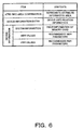
- the data recorded in the attribute information area has the meaning shown in Fig.6.
- identification codes for identifying the attribute information area.
- the "Device-information entry” indicates each recording position of the following "Device-information (System information, MBR Values, MBR Values and PBR Values)".
- the recording positions are represented by offset values of the attribute information area.
- System information there is recorded the internal information of the present memory card 1.
- version information For example, in the “System information”, there are recorded the version, class information, number of bytes in one block, number of sectors in one block, total number of blocks, date and time of assembling, serial numbers, assembly maker numbers, flash memory maker numbers, flash memory model numbers, controller numbers, controller functions, start sector numbers of the block boundaries and device types (read/write feasibility, read-only etc.).
- 'MBR' ('Master Boot Record') prescribed on the MS-DOS.
- boot identification For example, in the "MBR Values”, there are recorded boot identification, start header number, start cylinder number, system identification, ultimate header number, ultimate sector number, ultimate cylinder number, start LBA sector number and the partition size to be recorded in the MBR.
- the sector indicated in the start LBA sector number becomes the recording position for the 'PBR (Partition Boot Record)', that is, the start position of each partition prescribed on the MS-DOS.
- 'PBR Partition Boot Record
- the present invention is not limited to application to a memory card having formed only a sole partition, but may be applied to a memory card having formed plural partitions.
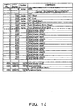
- PBR Values there are recorded recommended parameters of 'PBR' prescribed on the MS-DOS. For example, there are recorded in the "PBR Values” the jump codes recorded in the PBR, names of OEM, versions, number of bytes per sector, number of sectors per cluster, number of reserved sectors, number of FATs (number of file allocation tables), number of root directory entries, number of sectors in a medium, medium IDs, number of sectors per head, number of heads, number of hidden sectors, total number of logical sectors, physical drive numbers, expansion boot identification, volume serial numbers, volume head or file system types.
- the jump codes recorded in the PBR the jump codes recorded in the PBR, names of OEM, versions, number of bytes per sector, number of sectors per cluster, number of reserved sectors, number of FATs (number of file allocation tables), number of root directory entries, number of sectors in a medium, medium IDs, number of sectors per head, number of heads, number of hidden sectors, total number of logical sectors, physical drive numbers, expansion boot identification, volume serial numbers, volume head or file
- a command for reading out the attribute information (READ_ATRB) is set as a control command.
- the host device 2 reads out the "MBR Values” and the "PBR Values” using the READ_ATRB command to render it possible to initialize the memory card 1 with the logical format recommended by the assembly maker.
- a command (FORMAT) for initializing the non-volatile semiconductor memory 17, as a control command.
- the memory I/F controller 16 refers to the "MBR Values" and the "PBR Values" recorded in the attribute information area in order to initialize the non-volatile semiconductor memory 17 in accordance with the contents of the "MBR Values" and the "PBR Values". The initialization of the memory card 1 will be explained in detail subsequently.
- the memory card 1 of the present invention uses the MS-DOS convertible format, as the logical format for the data storage area.
- the MS-DOS convertible format is a file system for supervising the data files recorded in a medium by a hierarchical directory structure.
- access to data on the medium is made in terms of what is called a cylinder, a head and a sector as a unit.
- the actual data readout/write unit to the medium is the sector.
- the MS-DOS convertible format provides a unit, called a cluster, for supervising the recorded data.
- the cluster size is a multiple of the sector size. For example, 64 sectors make up a cluster. From the operating system on the side of the host device 2, file management is made on the cluster basis.
- the cluster size is smaller than the block size and moreover n times the cluster size, where n is an integer not less than two, becomes the size of one block.
- n is an integer not less than two
- the logical format applied to the memory card 1 of the present invention is set so that the boundary position of a block necessarily coincides with the boundary position of the cluster. That is, the setting is such that one cluster is not astride two blocks.
- the recording positions of the file management data of the MS-DOS such as MBR, PBR, FAT or route directories, or parameters recorded in the respective file management data.
- the parameters for implementing the logical format under the above conditions are recorded in the "MBR Values" and in the "PBR Values" in the attribute information.
- the contents of the file management data of the MS-DOS file are as follows:
- the MBR is recorded at the leading end of a user area.
- the contents stated in the MBR are the same as those stated in the "MBR Values" in the attribute information.
- the PBR is stated in a leading sector of each partition.
- the sector where the PBR is recorded is stated in the start LBA sector number in the MBR.
- the LBA sector number is the number uniquely accorded to the respective sectors in the effective blocks or in the substitution blocks for the effective blocks.
- the LBA sector numbers are accorded in the rising order beginning from the leading sector of the block having the logical block number of 0.
- the FAT is recorded over plural sectors beginning from a sector next following the PBR.
- the FAT represents the connecting state of files, handled in the user area, in terms of clusters as units.
- the data recorded on the medium are managed in terms of clusters as units. If the main body of a file is astride plural files, it is necessary to read out a cluster to its end and subsequently to read out the next cluster. However, the next cluster is not necessarily recorded in the physically consecutive positions. Thus, in accessing data recorded on a medium, the host device 2 is in need of the information indicating which is the cluster next following a given cluster. It is in the FAT that this sort of the information is recorded.
- the FAT is provided with as many storage areas as there are the clusters on the medium.
- the cluster numbers beginning from 02 hex , are accorded to the totality of the clusters present on the medium.
- To the respective storage areas in the FAT there are uniquely accorded the cluster numbers.
- In each of these storage areas there is stored the number of the cluster next following the cluster to which the storage area is allocated. Thus, if desired to find out the next cluster connected to a given cluster, it is sufficient to refer to the number stored in the storage area associated with the cluster in question.
- the present memory card 1 records two FATs (FAT1, FAT2) for backup.
- the physical data size of a given FAT is necessarily constant, even if the data contents are updated, because the number of clusters in the medium is unchanged.
- a route directory entry there is recorded the entry information of each file and each sub-directory arranged in a root directory.
- the route directory entry is recorded as from the sector next following the last sector in which has been recorded the FAT.
- the number of bytes in a given entry information is of a prescribed value, while the number of the entries arranged in the route directory is also of a prescribed value. Consequently, the data size of the route directory entry is necessarily constant.
- the route directory entry is not handled separately and is placed under cluster management.
- the first cluster (cluster number "02") is initiated as from the sector next following the above-described file management data. That is, the sectors as from the last sector in which has been recorded the route directory entry becomes an area where the actual files generated by the user are recorded.
- the above file management data are recorded in the present memory card 1 so that the first sector of the cluster number 02 necessarily becomes the leading sector of the block.
- the LBA sector number of the leading sector of a given block in the user area is stated in the 'start sector number of the block boundary' in the attribute information.
- the format termed a so-called super-floppy system may be applied to the memory card 1 of the present invention.
- the super-floppy system no management data corresponding to the aforementioned MBR is provided and the PBR is recorded at the leading end of the user area.
- the present invention may be applied to a format where there is no MBR such as that of the super-floppy system, in addition to the MS-DOS convertible format.
- the memory card 1 of the present invention For enabling the memory card 1 of the present invention to be referenced from the operation system of the host device 2, the memory card 1 needs to be initialized by the filing system of the MS-DOS. For initializing processing, it is sufficient to record at least the file management system (MBR, PBR, FAT or route directory entry). This initializing processing, routinely performed at the time of shipment of the memory card 1, may also be performed by the user as necessary.
- MLR file management system
- the first method is to write necessary data in a predetermined sector, using the control command for writing.
- the second method is using the control command for initialization.
- the memory card 1 it is determined on the interfacing protocol that an operation controlling command is transferred from the host device 2 to the memory I/F controller 16.
- the control command is stored in a command register in the register circuit 13 by a command set command in the TPC from the host device 2, in a command register in the register circuit 13. If once the control command is stored in the command register, the memory I/F controller 16 executes the operation control in keeping with the control command.
- the control command may be enumerated by a command for reading out data from the non-volatile semiconductor memory 17 to the data buffer circuit 14, a command for writing data from the data buffer circuit 14 to the non-volatile semiconductor memory 17, a command for erasing data on the non-volatile semiconductor memory 17, a formatting command for restoring the present memory card 1 to the state at the time of shipment from the plant, and a sleep command for halting the operation of an oscillator 18 of the memory card 1.
- a READ_DATA command is a command for reading out data in succession from specified addresses in the user area of the non-volatile semiconductor memory 17.
- the memory I/F controller 16 references an address stored in an address register in the register circuit 13 to access the address on the non-volatile semiconductor memory 17 to read out the data from this address.
- the data so read out are temporarily transferred to the data buffer circuit 14. If once the data buffer circuit 14 is full, that is if 512 bytes have been read out, the memory I/F controller 16 issues a transfer request interrupt for the host device 2.
- the data in the data buffer circuit 14 is read out by the host device 2, the next following data are transmitted from the non-volatile semiconductor memory 17 to the data buffer circuit 14.
- the memory I/F controller 16 repeats the aforementioned processing until a number of data corresponding to the number of data stored in a data count register in the register circuit 13 has been read out.
- the WRITE_DATA command is a command for recording data stored in the data buffer circuit 14 in succession as from the specified address in the user area of the non-volatile semiconductor memory 17. If the WRITE_DATA command is supplied, the memory I/F controller 16 refers to the address stored in the data address register in the register circuit 13 to access the address on the non-volatile semiconductor memory 17 to write data as from this address.
- the data written is the data stored in the data buffer circuit 14.
- the memory I/F controller 16 issues a transfer request interrupt to the host device 2.
- the data has been written in the data buffer circuit 14 by the host device 2
- the next following data are written from the data buffer circuit 14 to the non-volatile semiconductor memory 17.
- the memory I/F controller 16 repeats the above processing until writing a number of data corresponding to the number of data stored in the data count register in the register circuit 13.
- the READ_ATRB is a command for reading out the attribute information from the non-volatile semiconductor memory 17.
- the memory I/F controller 16 reads out the attribute information in the non-volatile semiconductor memory 17 to transfer the data so read out to the data buffer circuit 14.
- the FORMAT command reads out the attribute information from the non-volatile semiconductor memory 17, while reading out "MBR Values” and "PBR Values” in this attribute information to write MBR, PBR, FAT and the route directory entry in the non-volatile semiconductor memory 17 in accordance with the read-out values.
- the host device 2 reads out the "MBR Values” and "PBR Values” in the attribute information, using the READ_ATRB command.
- the host device 2 refers to the values stated in the "MBR Values” and “PBR Values” to generate MBR, PBR, FAT and the route directory.
- the host device 2 writes the so generated MBR, PBR, FAT and the route directory entry in predetermined sectors stated in the "MBR Values" and "PBR Values", using the WRITE_DATA command.
- the memory card 1 is initialized so that it can be referenced by the host device 2.
- the values of the MBR, PBR, FAT and the route directory entry need not be equal to the "MBR Values" or the "PBR Values" in the attribute information and may be uniquely generated by the host device 2.
- the host device 2 sends the FORMAT command to the memory I/F controller 16 of the host device 2.
- the memory I/F controller 16 reads out the "MBR Values” or the "PBR Values” in the attribute information. Based on the values stated in the so read out "MBR Values” or the "PBR Values", the memory I/F controller 16 writes the MBR, PBR, FAT and the route directory entry in the predetermined sectors in the non-volatile semiconductor memory 17.
- the memory card 1 is initialized so that it can be referenced by the host device 2.
- the memory card 1 of the present invention it is possible to selectively perform the two sorts of the initialization, namely a method in which the host device 2 writes the parameters generated by the host device 2 itself, by way of initialization, using the write command (WRITE_DATA command), and a method in which the host device 2 uses a command for initialization (FORMAT command) and in which the memory card 1 automatically performs the initialization.
- the host device 2 is able to use the command for initialization (FORMAT command), so that it is unnecessary for dedicated parameters or an initializing program conforming to the versions or the standards to be enclosed with the result that the initialization can be achieved extremely readily.
- the host device When the memory card 1 is loaded in the slot of the host device 2, the host device reads out the 'number of sectors contained in one block' and the 'start sector number of the block boundary' from the "System information" in the attribute information, using the command for reading out the attribute information (READ_ATRB command) (step S11).
- the host device 2 then is in a standby state until the recording operation is started by the user (step S12).
- the host device 2 checks whether the current recording mode is the real-time recording mode or the usual recording mode (step S13).
- processing transfers to a step S14 and, in case the recording mode is the real-time recording mode, processing transfers to a step S15.
- the real-time recording mode is such a mode in which data recording operation must follow the recording data generating processing as in case of real-time recording of moving picture signals, or in which recording processing needs high speed recording, as in case of recording large volume data.
- the usual recording mode is such a recording mode in which high speed recording is not needed, as in case of recording a still image.
- the mode selection of selecting the real-time recording or the usual recording may be manually set by the user or may also be automatically set in meeting with the data recording by the host device 2.
- a step S14 recording processing is carried out on the cluster basis. That is, the FAT is referenced to retrieve a void area on the cluster basis to record data sequentially in the void area found out.
- a step S15 the FAT is referenced to find out a void area which is continuously void for one block interval. If there is such void area which is continuously void for one block interval, data is recorded in such block in succession. That is, should there be a void cluster, but data has already been recorded in another cluster of the block to which belongs the void cluster, no data is recorded in the void cluster. For example, if one block is made up by four clusters, data is recorded in the void cluster on the four-cluster basis.
- the host device 2 usually is unable to recognize a block on the physical format.
- the logical format is formed so that the block boundary position is necessarily the cluster boundary position.
- the block can be recognized from the logical format.
- the host device 2 is able to verify the number of clusters in one block and the position of the leading cluster in the block from the 'number of sectors contained in one block' and the 'start sector number of the block boundary' referenced in the step S11.
- this real-time recording mode is applied, data can be recorded on the block basis, even for a medium in which the erasure block is larger in size than the cluster size, without employing a special file system.
- data can be recorded without generating the garbage collection which is necessary for protecting the recorded data, and hence recording can be carried out more speedily than if the data is recorded on the cluster basis as usual.
- the host device 2 simply detects the number of void clusters form the FAT to calculate the void capacity. If conversely the real-time recording mode is selected, simply the number of void clusters is detected from the FAT to calculate the void capacity. If conversely the real-time recording mode has been selected, such a block in which the totality of the clusters are unrecorded is detected from the FAT and the void capacity is calculated from the number of the blocks.
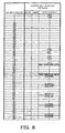
- a specified instance of formatting of the memory card 1 is now shown.
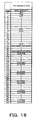
- the formatting instance now explained, is for the memory card 1 in which the total capacity is 64 Mbytes, the sector size is 512 bytes, the cluster size is 32 Kbytes, a block size is 128 Kbytes and the number of sectors needed for recording one FAT is eight.
- each cluster is made up by 64 sectors, with each block being made up by four clusters.
- FAT 16 used in case the total number of clusters exceeds 4085, as an MS-DOS type, is explained.
- the number of bytes allocated to each cluster in the FAT is 2 bytes (16 bits).
- Fig.8 shows an image of a medium of a first specified example.
- Fig.9 shows the values of respective parameters of the first specified instance.
- Figs.10 and 11 show the contents of description of the MBR and the PBR of the first specified instance, respectively.
- the LBA sector number is a number uniquely attached to the totality of the effective blocks in the medium, without regard to the partitions or boot areas.
- the leading sector number is 0, and is sequentially incremented by 1.
- the block number is the logical block number accorded to each effective block.
- the leading block is 0 and is sequentially incremented by 1. Meanwhile, in case of substitution of the effective blocks, the LBA sector number and the block number are accorded to the substituted blocks.
- the MBR is recorded in the leading sector of the block number 0 (with the LBA sector number of 0).
- the PBR is recorded in the sector of the LBA sector number 462 of the block number 1.
- the FAT1 and the FAT2 are recorded in the sectors of the LBA sector numbers 464 to 479 of the block number 1.
- the route directory entry is recorded in the sectors with the sector numbers of 480 to 511 of the block number 1.
- the leading sector (leading sector of the cluster 2) where there is recorded the file generated by the user is recorded as from the leading sector of the block 2 (LBA sector number 512).
- the logical format is such a one in which the block boundary position is coincident with the cluster boundary position.
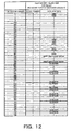
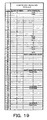
- Fig.12 shows an image of a medium of the second specified instance.
- Fig.13 shows the values of respective parameters of the second specified instance.
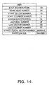
- Figs. 14 and 15 show the contents of description of the MBR and the PBR of the second specified instance, respectively.
- the LBA sector number is a number uniquely attached to each of the effective blocks in the medium, without regard to the partitions or boot areas.
- the leading sector number is 0, and is sequentially incremented by 1.
- the block number is the logical block number accorded to the respective effective blocks.
- the leading block is 0 and is sequentially incremented by 1. Meanwhile, in case of substitution of the effective blocks, the LBA sector number and the block number are accorded to the substituted blocks.
- the MBR is recorded in the leading sector of the block number 0 (with the LBA sector number of 0).
- the PBR is recorded in the sector of the LBA sector number of 335 of the block number 1.
- the FAT1 and the FAT2 are recorded in the sectors of the LBA sector numbers 336 to 351 of the block number 1.
- the route directory entry is recorded in the sectors with the sector numbers of 352 to 383 of the block number 1.
- the leading sector (leading sector of the cluster 2), where the file generated by the user is recorded, is recorded as from the LBA sector number 384 of the block 1.
- the logical format is such a one in which the block boundary position is coincident with the cluster boundary position.
- the block boundary position is the cluster boundary position and block-based batch recording may be made from the host device 2, that is, recording can be made on the four-cluster basis.
- the leading eight bytes are of a prescribed value of "F8FF FFFF".
- the FAT16 format also prescribes the area of each cluster every four bytes as from the ninth byte.
- the cluster number of the first cluster is "2". In the present instance, the number of bytes per sector is 512.
- a cluster area from the cluster number 2 to the cluster number 127 is formed.
- the block 2 is formed by the cluster numbers of 02, 03, 04 and 05
- the block 3 is formed by the cluster numbers of 06, 07, 08 and 09
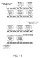
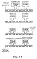
- the block 4 is formed by the cluster numbers of 0a, 0b, 0c and 0d and so forth, so that, subsequently, each one block is formed by four clusters, as shown in Fig.16.
- the leading sector of the FAT ends with the second cluster (cluster 7f) of the block 33.
- the second sector of the FAT begins with the third cluster (cluster 80) of the block 33. That is, in the format of the first specified instance, the block boundary represented in the FAT is not coincident with the actual sector position of the FAT.
- the block 1 is formed by the cluster numbers of 02 and 03
- the block 2 is formed by the cluster numbers of 04, 05, 06 and 07
- the block 3 is formed by the cluster numbers of 08, 09, 0a and 0b
- the block 4 is formed by the cluster numbers of 0c, 0d, 0e and 0f, and so forth, so that, subsequently, each one block is formed by four clusters, as shown in Fig.17.
- the leading sector of the FAT ends with the fourth cluster of the block 32, that is the last cluster in the block (cluster 7f).
- the second sector of the FAT begins with the first cluster of the block 33. That is, in the format of the second specified instance, the block boundary position represented in the FAT is coincident with the actual sector position of the FAT.
- the file management on the side of the host device 2 is easier with the format of the second specified instance than with the format of the first specified instance.
- the MBR is recorded in a sole block. That is, the MBR is recorded in a block different than the PBR, FAT or the route directory entry.
- the MBR is recorded in the sole block, it becomes possible to provide for file safety in case of a medium where a batch erasure unit is fixed, as in a flash memory. That is, since the MBR is recorded in the PBR, FAT or root directory entry that is liable to be rewritten or in a block different from real data, it becomes unnecessary to rewrite MBR, thus assuring the file safety.
- This recording of the MBR in a block different than the block in which to record the PBR, FAT or the route directory entry may be applied even in a case different from the case of the present memory card 1 in which the block size is larger than the cluster size.
- the MBR, PBR, FAT and the route directory entry are recorded in succession on the sector basis, without regard to the block position, as shown in Fig.18. That is, the MBR and the PBR are recorded in the sector of sector number 0 and in the sector of sector number 1, respectively.
- the cluster size is smaller than the block size, as when the cluster size is 32 Kbytes and the block size is 16 Kbytes, it is sufficient if the MBR is recorded in the sector of the sector number 0 and the PBR is recorded in the sector of the sector number 47, as shown in Fig. 19.
- the MBR is recorded in the sector of the sector number 0 and the PBR is recorded in the sector of the sector number 79, as shown in Fig. 20.
- the file management data for logical formatting may be recorded on a semiconductor memory, depending on parameters stored in the data storage device, when an initialization command is received from a host device, so that the initialization can be achieved extremely readily without the host device having to be provided with a control program or parameters for initialization.
Landscapes
- Engineering & Computer Science (AREA)
- Theoretical Computer Science (AREA)
- Physics & Mathematics (AREA)
- General Physics & Mathematics (AREA)
- General Engineering & Computer Science (AREA)
- Human Computer Interaction (AREA)
- Microelectronics & Electronic Packaging (AREA)
- Business, Economics & Management (AREA)
- Computer Networks & Wireless Communication (AREA)
- Accounting & Taxation (AREA)
- Strategic Management (AREA)
- General Business, Economics & Management (AREA)
- Information Retrieval, Db Structures And Fs Structures Therefor (AREA)
Applications Claiming Priority (3)
| Application Number | Priority Date | Filing Date | Title |
|---|---|---|---|
| JP2002112635 | 2002-04-15 | ||
| JP2002112635A JP4206688B2 (ja) | 2002-04-15 | 2002-04-15 | データ処理装置及びデータ処理方法 |
| PCT/JP2003/004708 WO2003088043A1 (fr) | 2002-04-15 | 2003-04-14 | Appareil de stockage de donnees |
Publications (2)
| Publication Number | Publication Date |
|---|---|
| EP1496437A1 true EP1496437A1 (fr) | 2005-01-12 |
| EP1496437A4 EP1496437A4 (fr) | 2008-07-30 |
Family
ID=29243324
Family Applications (1)
| Application Number | Title | Priority Date | Filing Date |
|---|---|---|---|
| EP03746481A Ceased EP1496437A4 (fr) | 2002-04-15 | 2003-04-14 | Appareil de stockage de donnees |
Country Status (6)
| Country | Link |
|---|---|
| US (1) | US7039754B2 (fr) |
| EP (1) | EP1496437A4 (fr) |
| JP (1) | JP4206688B2 (fr) |
| KR (1) | KR100980905B1 (fr) |
| CN (1) | CN1297900C (fr) |
| WO (1) | WO2003088043A1 (fr) |
Cited By (9)
| Publication number | Priority date | Publication date | Assignee | Title |
|---|---|---|---|---|
| WO2008082999A3 (fr) * | 2006-12-26 | 2008-10-02 | Sandisk Corp | Configuration d'interface lba hôte comprenant une mémoire flash |
| EP1746491A4 (fr) * | 2004-05-07 | 2009-05-06 | Panasonic Corp | Procédé pour l'accession à des données, appareil et support d'enregistrement pour réaliser ce procédé |
| US7581057B2 (en) | 2005-08-03 | 2009-08-25 | Sandisk Corporation | Memory system with management of memory blocks that directly store data files |
| US7739444B2 (en) | 2006-12-26 | 2010-06-15 | Sandisk Corporation | System using a direct data file system with a continuous logical address space interface |
| US7917686B2 (en) | 2006-12-26 | 2011-03-29 | Sandisk Corporation | Host system with direct data file interface configurability |
| US8046522B2 (en) | 2006-12-26 | 2011-10-25 | SanDisk Technologies, Inc. | Use of a direct data file system with a continuous logical address space interface and control of file address storage in logical blocks |
| US8166267B2 (en) | 2006-12-26 | 2012-04-24 | Sandisk Technologies Inc. | Managing a LBA interface in a direct data file memory system |
| US8209461B2 (en) | 2006-12-26 | 2012-06-26 | Sandisk Technologies Inc. | Configuration of host LBA interface with flash memory |
| EP2177994A4 (fr) * | 2007-08-10 | 2013-08-21 | Panasonic Corp | Support amovible, dispositif, système, procédé et programme de formatage |
Families Citing this family (43)
| Publication number | Priority date | Publication date | Assignee | Title |
|---|---|---|---|---|
| JP4079506B2 (ja) * | 1997-08-08 | 2008-04-23 | 株式会社東芝 | 不揮発性半導体メモリシステムの制御方法 |
| US20030229472A1 (en) * | 2001-12-06 | 2003-12-11 | Kantzes Christopher P. | Field maintenance tool with improved device description communication and storage |
| US10261506B2 (en) * | 2002-12-05 | 2019-04-16 | Fisher-Rosemount Systems, Inc. | Method of adding software to a field maintenance tool |
| DE112004000385T5 (de) | 2003-03-06 | 2006-02-16 | Fisher-Rosemount Systems Inc. | Wärmefluss-regulierende Abdeckung für eine elektrische Speicherzelle |
| US7512521B2 (en) * | 2003-04-30 | 2009-03-31 | Fisher-Rosemount Systems, Inc. | Intrinsically safe field maintenance tool with power islands |
| US8874402B2 (en) * | 2003-05-16 | 2014-10-28 | Fisher-Rosemount Systems, Inc. | Physical memory handling for handheld field maintenance tools |
| US7526802B2 (en) * | 2003-05-16 | 2009-04-28 | Fisher-Rosemount Systems, Inc. | Memory authentication for intrinsically safe field maintenance tools |
| JP4773828B2 (ja) * | 2004-01-26 | 2011-09-14 | パナソニック株式会社 | 半導体メモリ装置 |
| JP2005222201A (ja) * | 2004-02-04 | 2005-08-18 | Matsushita Electric Ind Co Ltd | メモリアクセス装置、及び半導体メモリカード |
| JP4874588B2 (ja) * | 2004-07-12 | 2012-02-15 | 株式会社東芝 | 記憶デバイスおよびホスト機器 |
| BRPI0510494B8 (pt) | 2004-07-12 | 2022-06-28 | Kk Toshiba Toshiba Corporation | Dispositivo de armazenagem e aparelho hospedeiro |
| JP2006085380A (ja) | 2004-09-15 | 2006-03-30 | Toshiba Corp | ファイルストレージデバイス、プログラム、及び不揮発性半導体メモリの書込方法 |
| US7949665B1 (en) * | 2004-11-19 | 2011-05-24 | Symantec Corporation | Rapidly traversing disc volumes during file content examination |
| JP4689247B2 (ja) * | 2004-11-19 | 2011-05-25 | キヤノン株式会社 | カメラ及びその制御方法 |
| US7412560B2 (en) | 2004-12-16 | 2008-08-12 | Sandisk Corporation | Non-volatile memory and method with multi-stream updating |
| US7315916B2 (en) * | 2004-12-16 | 2008-01-01 | Sandisk Corporation | Scratch pad block |
| US9639554B2 (en) | 2004-12-17 | 2017-05-02 | Microsoft Technology Licensing, Llc | Extensible file system |
| US20060253643A1 (en) * | 2005-05-04 | 2006-11-09 | Delkin Devices, Inc. | Memory with isolated master boot record |
| US8051270B2 (en) * | 2005-05-23 | 2011-11-01 | Panasonic Corporation | Memory controller, nonvolatile storage device, nonvolatile storage system, and memory control method |
| KR100739722B1 (ko) * | 2005-08-20 | 2007-07-13 | 삼성전자주식회사 | 플래시 메모리 관리 방법 및 플래시 메모리 시스템 |
| KR100823171B1 (ko) * | 2007-02-01 | 2008-04-18 | 삼성전자주식회사 | 파티션된 플래시 변환 계층을 갖는 컴퓨터 시스템 및플래시 변환 계층의 파티션 방법 |
| KR100923990B1 (ko) * | 2007-02-13 | 2009-10-28 | 삼성전자주식회사 | 플래시 저장 장치의 특성을 기반으로 한 컴퓨팅 시스템 |
| KR101395778B1 (ko) * | 2007-03-14 | 2014-05-19 | 삼성전자주식회사 | 메모리 카드 및 그것을 포함하는 메모리 시스템 그리고그것의 동작 방법 |
| JP4985108B2 (ja) * | 2007-05-30 | 2012-07-25 | ソニー株式会社 | データ記憶装置およびその制御方法 |
| CN102385346B (zh) * | 2007-06-13 | 2015-07-29 | 费希尔-罗斯蒙德系统公司 | 手持现场维护工具的改进功能 |
| JP4575410B2 (ja) * | 2007-08-29 | 2010-11-04 | 株式会社東芝 | 半導体記憶装置およびその動作方法 |
| US7797818B2 (en) * | 2007-09-13 | 2010-09-21 | Sony Ericsson Mobile Communications Ab | Flexible modular systems for constructing a wireless communication terminal |
| JP4551940B2 (ja) | 2008-03-01 | 2010-09-29 | 株式会社東芝 | メモリシステム |
| TWI452467B (zh) * | 2008-10-13 | 2014-09-11 | A Data Technology Co Ltd | 記憶體系統及其控制方法 |
| CN102202132B (zh) * | 2010-03-24 | 2013-06-05 | 中兴通讯股份有限公司 | 一种对上网设备进行初始化的方法、系统及设备 |
| JP2012019383A (ja) * | 2010-07-08 | 2012-01-26 | Panasonic Corp | 記録制御装置、半導体記録装置および記録システム |
| TWI420305B (zh) * | 2010-10-08 | 2013-12-21 | Phison Electronics Corp | 記憶體儲存裝置、其記憶體控制器與自動產生填充檔案的方法 |
| CN101958152B (zh) * | 2010-10-19 | 2013-02-13 | 华中科技大学 | 一种nand flash控制器及其应用 |
| CN107252786B (zh) * | 2012-02-05 | 2019-11-01 | 麦修斯资源有限公司 | 输送系统和将数据与输送系统正运送的物品相关联的方法 |
| CN103425539B (zh) * | 2012-05-14 | 2016-04-27 | 联想(北京)有限公司 | 信息处理方法及装置 |
| CN103942219A (zh) * | 2013-01-22 | 2014-07-23 | 鸿富锦精密工业(深圳)有限公司 | 存储卡分区系统及方法 |
| CN103150125B (zh) * | 2013-02-20 | 2015-06-17 | 郑州信大捷安信息技术股份有限公司 | 提高掉电保护数据缓冲存储器使用寿命的方法及智能卡 |
| TWI676176B (zh) * | 2018-10-25 | 2019-11-01 | 群聯電子股份有限公司 | 資料整併方法、記憶體儲存裝置及記憶體控制電路單元 |
| US10936454B2 (en) | 2018-11-21 | 2021-03-02 | International Business Machines Corporation | Disaster recovery for virtualized systems |
| JP7278083B2 (ja) * | 2019-01-24 | 2023-05-19 | 凸版印刷株式会社 | 半導体装置、制御方法、およびプログラム |
| TWI777111B (zh) * | 2019-12-18 | 2022-09-11 | 點序科技股份有限公司 | 雙接頭記憶體裝置以及傳輸控制電路 |
| CN113918081B (zh) * | 2020-07-08 | 2024-03-26 | 慧荣科技股份有限公司 | 计算机可读取存储介质、配置可靠命令的方法及装置 |
| US12112052B2 (en) * | 2022-03-30 | 2024-10-08 | Micron Technology, Inc. | Reading a master boot record for a namespace after reformatting the namespace |
Family Cites Families (12)
| Publication number | Priority date | Publication date | Assignee | Title |
|---|---|---|---|---|
| JPH01286016A (ja) * | 1988-05-13 | 1989-11-17 | Canon Electron Inc | 情報記録再生装置 |
| JPH04238194A (ja) * | 1991-01-21 | 1992-08-26 | Sharp Corp | 半導体メモリ |
| JPH06309527A (ja) * | 1993-04-26 | 1994-11-04 | Matsushita Electric Ind Co Ltd | Icカード |
| WO1998025239A1 (fr) * | 1996-12-03 | 1998-06-11 | Strategic Analysis, Inc. | Procede et dispositif de formatage de carte a puce et de lecteur de carte |
| JP3365283B2 (ja) * | 1997-11-14 | 2003-01-08 | 日本電気株式会社 | 半導体記憶装置 |
| JPH11282630A (ja) * | 1998-03-27 | 1999-10-15 | Hitachi Koki Co Ltd | ハードディスクドライブのフォーマッティング方式 |
| JP2000267904A (ja) * | 1999-03-17 | 2000-09-29 | Sanyo Electric Co Ltd | データ記録装置及び方法 |
| US6687814B1 (en) * | 1999-07-12 | 2004-02-03 | Micron Technology, Inc. | Controller with interface attachment |
| JP3249959B2 (ja) * | 1999-10-12 | 2002-01-28 | 株式会社ソニー・コンピュータエンタテインメント | 可搬型記憶装置及びメモリカード |
| CN100442393C (zh) * | 1999-10-21 | 2008-12-10 | 松下电器产业株式会社 | 半导体存储卡的访问装置、初始化方法和半导体存储卡 |
| US6601056B1 (en) * | 2000-09-28 | 2003-07-29 | Microsoft Corporation | Method and apparatus for automatic format conversion on removable digital media |
| JP3595935B2 (ja) | 2000-10-02 | 2004-12-02 | 和夫 松久 | 播種の名札 |
-
2002
- 2002-04-15 JP JP2002112635A patent/JP4206688B2/ja not_active Expired - Fee Related
-
2003
- 2003-04-14 KR KR1020037016270A patent/KR100980905B1/ko not_active Expired - Fee Related
- 2003-04-14 US US10/480,706 patent/US7039754B2/en not_active Expired - Lifetime
- 2003-04-14 CN CNB038004356A patent/CN1297900C/zh not_active Expired - Fee Related
- 2003-04-14 WO PCT/JP2003/004708 patent/WO2003088043A1/fr not_active Ceased
- 2003-04-14 EP EP03746481A patent/EP1496437A4/fr not_active Ceased
Cited By (11)
| Publication number | Priority date | Publication date | Assignee | Title |
|---|---|---|---|---|
| EP1746491A4 (fr) * | 2004-05-07 | 2009-05-06 | Panasonic Corp | Procédé pour l'accession à des données, appareil et support d'enregistrement pour réaliser ce procédé |
| US7631140B2 (en) | 2004-05-07 | 2009-12-08 | Panasonic Corporation | Data accessing method, device in which the data accessing method is executed and recording medium |
| US7581057B2 (en) | 2005-08-03 | 2009-08-25 | Sandisk Corporation | Memory system with management of memory blocks that directly store data files |
| US8055832B2 (en) | 2005-08-03 | 2011-11-08 | SanDisk Technologies, Inc. | Management of memory blocks that directly store data files |
| WO2008082999A3 (fr) * | 2006-12-26 | 2008-10-02 | Sandisk Corp | Configuration d'interface lba hôte comprenant une mémoire flash |
| US7739444B2 (en) | 2006-12-26 | 2010-06-15 | Sandisk Corporation | System using a direct data file system with a continuous logical address space interface |
| US7917686B2 (en) | 2006-12-26 | 2011-03-29 | Sandisk Corporation | Host system with direct data file interface configurability |
| US8046522B2 (en) | 2006-12-26 | 2011-10-25 | SanDisk Technologies, Inc. | Use of a direct data file system with a continuous logical address space interface and control of file address storage in logical blocks |
| US8166267B2 (en) | 2006-12-26 | 2012-04-24 | Sandisk Technologies Inc. | Managing a LBA interface in a direct data file memory system |
| US8209461B2 (en) | 2006-12-26 | 2012-06-26 | Sandisk Technologies Inc. | Configuration of host LBA interface with flash memory |
| EP2177994A4 (fr) * | 2007-08-10 | 2013-08-21 | Panasonic Corp | Support amovible, dispositif, système, procédé et programme de formatage |
Also Published As
| Publication number | Publication date |
|---|---|
| JP2003308241A (ja) | 2003-10-31 |
| EP1496437A4 (fr) | 2008-07-30 |
| CN1516834A (zh) | 2004-07-28 |
| US7039754B2 (en) | 2006-05-02 |
| KR20040100847A (ko) | 2004-12-02 |
| WO2003088043A1 (fr) | 2003-10-23 |
| US20050036372A1 (en) | 2005-02-17 |
| KR100980905B1 (ko) | 2010-09-07 |
| CN1297900C (zh) | 2007-01-31 |
| JP4206688B2 (ja) | 2009-01-14 |
| WO2003088043B1 (fr) | 2004-05-13 |
Similar Documents
| Publication | Publication Date | Title |
|---|---|---|
| US7039754B2 (en) | Detachably mounted removable data storage device | |
| US7472251B2 (en) | Data storage apparatus detachably mounted to a host apparatus | |
| KR101033068B1 (ko) | 메모리 장치 및 그 메모리 장치를 이용한 기록 재생 장치 | |
| US20110231597A1 (en) | Data access method, memory controller and memory storage system | |
| CN101401076A (zh) | 针对具有可擦除/可重写存储器使用带有主机装置的一次或数次可编程存储器的方法及装置 | |
| US7681008B2 (en) | Systems for managing file allocation table information | |
| US7752412B2 (en) | Methods of managing file allocation table information | |
| CN103377143A (zh) | 存储器管理方法、存储器控制器与存储器存储装置 | |
| US20080250189A1 (en) | Circuit and Method for Improving Operation Life of Memory | |
| JP2007018528A (ja) | メモリ装置、ファイル管理方法及び記録再生装置 |
Legal Events
| Date | Code | Title | Description |
|---|---|---|---|
| PUAI | Public reference made under article 153(3) epc to a published international application that has entered the european phase |
Free format text: ORIGINAL CODE: 0009012 |
|
| 17P | Request for examination filed |
Effective date: 20031128 |
|
| AK | Designated contracting states |
Kind code of ref document: A1 Designated state(s): AT BE BG CH CY CZ DE DK EE ES FI FR GB GR HU IE IT LI LU MC NL PT RO SE SI SK TR |
|
| A4 | Supplementary search report drawn up and despatched |
Effective date: 20080701 |
|
| 17Q | First examination report despatched |
Effective date: 20081016 |
|
| REG | Reference to a national code |
Ref country code: DE Ref legal event code: R003 |
|
| STAA | Information on the status of an ep patent application or granted ep patent |
Free format text: STATUS: THE APPLICATION HAS BEEN REFUSED |
|
| 18R | Application refused |
Effective date: 20130924 |