EP1496528B1 - Oscillateur différentiel - Google Patents
Oscillateur différentiel Download PDFInfo
- Publication number
- EP1496528B1 EP1496528B1 EP04015456A EP04015456A EP1496528B1 EP 1496528 B1 EP1496528 B1 EP 1496528B1 EP 04015456 A EP04015456 A EP 04015456A EP 04015456 A EP04015456 A EP 04015456A EP 1496528 B1 EP1496528 B1 EP 1496528B1
- Authority
- EP
- European Patent Office
- Prior art keywords
- shield plate
- capacitor
- differential
- oscillation circuit
- vertical plane
- Prior art date
- Legal status (The legal status is an assumption and is not a legal conclusion. Google has not performed a legal analysis and makes no representation as to the accuracy of the status listed.)
- Expired - Lifetime
Links
Images




Classifications
-
- H—ELECTRICITY
- H10—SEMICONDUCTOR DEVICES; ELECTRIC SOLID-STATE DEVICES NOT OTHERWISE PROVIDED FOR
- H10W—GENERIC PACKAGES, INTERCONNECTIONS, CONNECTORS OR OTHER CONSTRUCTIONAL DETAILS OF DEVICES COVERED BY CLASS H10
- H10W20/00—Interconnections in chips, wafers or substrates
- H10W20/40—Interconnections external to wafers or substrates, e.g. back-end-of-line [BEOL] metallisations or vias connecting to gate electrodes
- H10W20/495—Capacitive arrangements or effects of, or between wiring layers
- H10W20/496—Capacitor integral with wiring layers
-
- H—ELECTRICITY
- H01—ELECTRIC ELEMENTS
- H01P—WAVEGUIDES; RESONATORS, LINES, OR OTHER DEVICES OF THE WAVEGUIDE TYPE
- H01P1/00—Auxiliary devices
- H01P1/20—Frequency-selective devices, e.g. filters
- H01P1/201—Filters for transverse electromagnetic waves
- H01P1/203—Strip line filters
-
- H—ELECTRICITY
- H01—ELECTRIC ELEMENTS
- H01Q—ANTENNAS, i.e. RADIO AERIALS
- H01Q1/00—Details of, or arrangements associated with, antennas
- H01Q1/52—Means for reducing coupling between antennas; Means for reducing coupling between an antenna and another structure
- H01Q1/526—Electromagnetic shields
-
- H—ELECTRICITY
- H01—ELECTRIC ELEMENTS
- H01Q—ANTENNAS, i.e. RADIO AERIALS
- H01Q15/00—Devices for reflection, refraction, diffraction or polarisation of waves radiated from an antenna, e.g. quasi-optical devices
- H01Q15/0006—Devices acting selectively as reflecting surface, as diffracting or as refracting device, e.g. frequency filtering or angular spatial filtering devices
- H01Q15/0013—Devices acting selectively as reflecting surface, as diffracting or as refracting device, e.g. frequency filtering or angular spatial filtering devices said selective devices working as frequency-selective reflecting surfaces, e.g. FSS, dichroic plates, surfaces being partly transmissive and reflective
-
- H—ELECTRICITY
- H01—ELECTRIC ELEMENTS
- H01Q—ANTENNAS, i.e. RADIO AERIALS
- H01Q23/00—Antennas with active circuits or circuit elements integrated within them or attached to them
Definitions
- the present invention relates to a differential oscillation circuit formed on a semiconductor substrate.
- a differential oscillation circuit is disclosed in the document US 2002/0171115 .
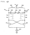
- FIG. 13 is a schematic diagram illustrating the structure of a commonly-used differential oscillation circuit 7.
- the differential oscillation circuit 7 comprises: first and second transistors 1001 and 1002 for enabling oscillation; first and second capacitors 1003 and 1004 for composing a differential capacitor and cutting off a DC component; first and second variable capacitors 1005 and 1006 for enabling resonance; first and second inductances 1007 and 1008 for enabling resonance; and a constant current source 1009.
- a DC current is supplied to the first and second inductances 1007 and 1008 of the differential oscillation circuit 7.
- the DC current is supplied to the first and second transistors 1001 and 1002, and thereafter flows to ground via the constant current source 1009.
- the first transistor 1001 is connected so as to realize positive feedback, and generates either one of an in-phase signal or a reverse-phase signal composing a differential pair of signals, having an oscillation frequency which depends on circuit constants of the first variable capacitor 1005 and the first inductance 1007.
- the second transistor 1002 which operates similarly to the first transistor 1001, generates the other one of the in-phase signal or the reverse-phase signal.
- the generated in-phase signal and reverse-phase signal are output from the Vo+ terminal and the Vo- terminal, respectively, or vice versa.
- FIG. 14A is an upper plan view illustrating the structure of a differential capacitor (the first capacitor 1003 and the second capacitor 1004) which is integrated on a semiconductor substrate.
- FIG. 18B is a cross-sectional view showing the first capacitor 1003 and the second capacitor 1004, taken along a vertical plane A-A' shown in FIG. 14A .
- the first capacitor 1003 and the second capacitor 1004 are to be formed within an interlayer film 1019 on a semiconductor substrate 1020, which is typically composed of p-type silicon.
- the interlayer film 1019 is typically composed of silicon oxide.
- the first capacitor 1003 includes an upper electrode 1015 and a lower electrode 1016, composed of metal wires which are typically aluminum.
- the upper electrode 1015 and the lower electrode 1016 are disposed parallel to each other, with a predetermined interval along the vertical direction.
- the second capacitor 1004 is composed of the same material as the first capacitor 1003, and includes an upper electrode 1017 and a lower electrode 1018, which are formed in symmetrical positions from the upper electrode 1015 and the lower electrode 1016, respectively, with respect to the predetermined vertical plane B-B'.
- the first capacitor 1003 and the second capacitor 1004 suffer fromthe aforementioned parasitic capacitances,which occur in the interlayer film 1019 between the semiconductor substrate 1020 and the lower electrodes 1016 and 1018, respectively. Furthermore, the aforementioned parasitic resistances also occur in the semiconductor substrate 1020. Among these parasitic components, the parasitic resistances occurring in the semiconductor substrate 1020 affect the quality factors of the resonator circuits in particular.
- FIG. 15A is an upper plan view schematically showing the structure of the conventional differential capacitor.
- FIG. 15B is a cross-sectional view showing the first capacitor 1003 and the second capacitor 1004, taken along a vertical plane A-A' shown in FIG. 15A .
- the conventional differential capacitor shown in FIGS. 15A and 15B differs from that shown in FIGS. 14A and 14B in that a shield plate 1021 is additionally comprised. Otherwise, the two differential capacitors are identical. Therefore, in FIGS. 15A and 15B , those component elements which have their counterparts in FIGS. 14A and 14B are denoted by the same reference numerals as those used therein, and the descriptions thereof are omitted.
- the shield plate 1021 which is a plate-like structural component composed of a conductive material such as aluminum, is disposed between the semiconductor substrate 1020 and the lower electrodes 1016 and 1018. More specifically, the shield plate 1021 has a shape such that, when the lower electrodes 1016 and 1018 are projected onto the shield plate 1021 from vertically above, the projected lower electrodes 1016 and 1018 appear as being contained within the outer contour of the shield plate 1021.
- the shield plate 1021 has a symmetrical shape with respect to the aforementioned vertical plane B-B'. With the shield plate 1021 as such, the parasitic capacitances in the interlayer film 1019 are increased, but the parasitic resistances in the semiconductor substrate 1020 are reduced.
- the sharpness of the resonance caused by each resonator circuit can be improved.
- the following parasitic components will appear in the differential oscillation circuit 7: a parasitic capacitance Cpa1 between the lower electrode 1016 and the shield plate 1021, a parasitic capacitance Cpa2 between the lower electrode 1018 and the shield plate 1021, a parasitic capacitance Cpc between the shield plate 1021 and the semiconductor substrate 1020, and a parasitic resistance Rpc in the semiconductor substrate 1020.
- a junction between the parasitic capacitances Cpa1 and Cpa2 serves as an apparent ground (hereinafter referred to as "virtual ground”) with respect to an AC signal.
- virtual ground an apparent ground
- the parasitic capacitances Cpa1 and Cpa2 would in effect be in parallel connection with the first variable capacitor 1005 and the second variable capacitor 1006. Moreover, since the parasitic capacitances Cpa1 and Cpa2 have fixed values, the amounts of capacitance variation in the first variable capacitor 1005 and the second variable capacitor 1006 would become smaller than their respective spec values, thus resulting in the oscillation frequency range of the differential oscillation circuit 7 being narrowed.
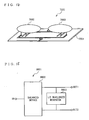
- FIG. 17 is a perspective view illustrating the structure of a conventional planar differential antenna element 7001.
- two planar antenna elements 7002 and 70003 which are disposed with a predetermined interval from each other on a silicon substrate 7004 (as one example of a semiconductor substrate), outputs an in-phase signal and a reverse-phase signal, which have the same power but have a 180° phase difference between each other.
- the differential antenna element 7001 can receive wide-band signals.
- the planar antenna elements 7002 and 7003 are formed on the silicon substrate 7004, the following problems will arise: coupling occurs due to a parasitic capacitance between the wiring and the silicon substrate 7004; and a loss occurs due to the influence of the parasitic resistance on the silicon substrate 7004. As a result, the gain of the differential antenna element 7001 will be deteriorated.
- FIG. 18 is a schematic diagram illustrating the structure of a balanced high-frequency device 8001 incorporating a conventional differential resonator.
- the balanced high-frequency device 8001 includes: an input terminal IN for receiving an input signal; a balanced device 8002 having output terminals OUT1 and OUT2 from which to output an in-phase signal and a reverse-phase signal; and a 1/2 wavelength resonator 8003 (as an example of a differential resonator) .
- the 1/2 wavelength resonator 8003 When receiving a signal having a predetermined frequency, the 1/2 wavelength resonator 8003 resonates so as to decrease an impedance of the in-phase signal component, which exists when the output terminals are viewed from the side of the balanced device 8002, so as to be lower than an impedance of the differential signal component which exists when the output terminals are viewed from the side of the balanced device 8002.
- the balanced high-frequency device 8001 suppresses the in-phase component, and improves the degree of balance between the output signals.
- the 1/2 wavelength resonator 8003 is formed on a silicon substrate (as an example of a semiconductor substrate) .
- the following problems will arise: coupling occurs due to a parasitic capacitance between the 1/2 wavelength resonator 8003 and the silicon substrate; and a loss occurs due to the influence of the parasitic capacitance on the silicon substrate.
- the insertion loss of the 1/2 wavelength resonator 8003 will increase.
- the at least one projected planar plate extends outside of the shield plate.
- the shield plate has a slit formed therein. More preferably, the slit intersects the vertical plane.
- the shield plate has a plurality of through-holes formed therein.
- an in-phase signal and a reverse-phase signal composing a differential pair of signals are respectively applied to the two terminals of the at least one planar plate.
- the shield plate is connected to ground via an inductance and/or a resistor.
- a portion of the shield plate that intersects the vertical plane is connected to ground.
- the differential oscillation circuit may be used in a filter circuit.
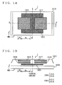
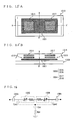
- FIG. 1A is a schematic diagram illustrating a differential capacitor 1 as viewed from vertically above.
- FIG. 1B is a schematic diagram showing a cross section of the differential capacitor 1 taken at a vertical plane A-A' in FIG. 1A , as viewed in the direction of arrow C.
- FIGS. 1A and 1B also show a three-dimensional coordinate system having three orthogonal axes of x, y, and z, where the z axis corresponds to the vertically upward direction, and the x and y axes correspond to the two respectively perpendicular directions on the horizontal plane. Note that the y axis is in the same direction as that of arrow C, and extends in parallel to a vertical plane B-B' described later.
- the differential capacitor 1 comprises a first capacitor 1003, a second capacitor 1004, and a shield plate 1022.
- the first and second capacitors 1003 and 1004 are formed within an interlayer film 1019 on the semiconductor substrate 1020.
- the semiconductor substrate 1020 and the interlayer film 1019 are identical to those described above in the "Description of the Background Art" section.
- the first capacitor 1003 and the second capacitor 1004 are composed of metal wires which are typically aluminum.
- the first capacitor 1003 includes an upper electrode 1015 and a lower electrode 1016, which lie substantially parallel to each other in the z-axis direction (i.e., the vertical direction) with a predetermined interval therebetween.
- the upper electrode 1015 and the lower electrode 1016 are formed in positions which are away from the vertical plane B-B' by a predetermined distance in a minus direction of the x axis.
- the second capacitor 1004 includes an upper electrode 1017 and a lower electrode 1018, which have substantially symmetrical configurations to those of the upper electrode 1015 and the lower electrode 1016, respectively, with respect to the vertical plane B-B'.
- the shield plate 1022 is a plate-like component composed of a conductive material such as aluminum, which has a symmetrical shape with respect to the vertical plane B-B' along the horizontal direction.
- the shield plate 1022 is interposed between the semiconductor substrate 1020 and both lower electrodes 1016 and 1018.
- the shield plate 1022 has a shape such that, when the lower electrodes 1016 and 1018 are projected onto the shield plate 1022 from vertically above, the projected lower electrodes 1016 and 1018 appear as partially overlapping with the shield plate 1022.
- the shield plate 1022 is shaped so that the projected lower electrodes 1016 and 1018 extend outside of the outer contour of the shield plate 1022.
- overlapping region Ao a portion of each of the lower electrodes 1016 and 1018 whose projected image overlaps with the shield plate 1022
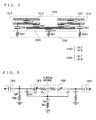
- FIG. 2 is a schematic diagram showing an equivalent circuit of the differential capacitor 1 shown in FIG. 1 .
- FIG. 2 shows, by a dotted line, a cross section of the differential capacitor 1 taken along the vertical plane A-A' .
- the first capacitor 1003 and the second capacitor 1004 each have a predetermined capacitance Cd.
- parasitic capacitances Cpa1 and Cpa2 occur between the shield plate 1022 and the lower electrodes 1016 and 1018, respectively.
- a parasitic capacitance Cpc and a parasitic resistance Rpc occur between the shield plate 1022 and the semiconductor substrate 1020.
- a parasitic capacitance Cpb1 and a parasitic resistance Rpb1 occur between the lower electrode 1016 and the semiconductor substrate 1020.
- a parasitic capacitance Cpb2 and a parasitic resistance Rpb2 occur between the lower electrode 1018 and the semiconductor substrate 1020.
- the non-overlapping region An (see FIGS. 15A and 15B and FIG. 16 ) is lacking, so that the parasitic capacitance Cpa1 occurring between the lower electrode 1016 and the shield plate 1021 would generally depend on the physical area of the lower electrode 1016 and the distance between the lower electrode 1016 and the shield plate 1021. This is also true of the conventional lower electrode 1018.
- the parasitic capacitance which is associated with the lower electrode 1016 generally depends on an area So of the overlapping region Ao, a distance Do between the overlapping region Ao and the shield plate 1022, an area Sn of the non-overlapping region An, and a distance Dn between the non-overlapping region An and the semiconductor substrate 1020. This is also true of the lower electrode 1018 of the differential capacitor 1.
- the parasitic capacitance which occurs per unit area of the lower electrode 1016 of the present differential capacitor 1 is smaller than that of the conventional lower electrode 1016, since the distance Dn is physically greater than the distance Do. This is also true of the lower electrode 1018 of the differential capacitor 1.
- the area of the overlapping region Ao may be reduced.
- reducing the overlapping region Ao would result in the parasitic capacitance Cpb1 being greater than the parasitic capacitance Cpa1, so that quality factor of the first capacitor 1003 would be greatly deteriorated due to the influence of the parasitic resistance Rpb1.
- a trade-off relationship exists between the parasitic capacitance of the lower electrode 1016 per unit area and the parasitic resistance Rpb1. If the differential capacitor 1 which is so susceptible to the influence of the parasitic resistance Rpb1 were to be applied to the differential oscillation circuit 7 (see FIG. 13 ), the quality factor of the entire circuit would be deteriorated.
- FIG. 3 is a schematic diagram showing the structure of a portion of a differential oscillation circuit 7 according to the invention, to which the present differential capacitor 1 is applied, this portion including the first and second capacitors 1003 and 1004 and the first and second variable capacitors 1005 and 1006. It is assumed that the first capacitor 1003 has the aforementioned capacitance Cd, and the first variable capacitor 1005 has a capacitance Cs.
- FIG. 3 shows the parasitic capacitances Cpa1 and Cpb1 and the parasitic resistance Rpb1 of the first capacitor 1003 as well as the parasitic resistance Rs of the first variable capacitor 1005.
- the aforementioned trade-off relationship will be described from the perspective of the capacitance variation ratio of the first variable capacitor 1005 and the quality factor of the circuit shown inFIG. 3.
- an in-phase signal and a reverse-phase signal are respectively supplied to the first capacitor 1003 and the second capacitor 1004, or vice versa.
- the differential oscillation circuit 7 has symmetry with respect to the virtual ground for AC signals (as indicated by a dot-dash line). Since the capacitance variation ratio and the quality factor of the second variable capacitor 1006 are therefore similar to those of the first variable capacitor 1005, the descriptions thereof are omitted.
- the virtual ground corresponds to a portion of the shield plate 1022 that intersects the vertical plane B-B'.
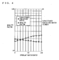
- FIG. 4 is a graph showing characteristic curves indicating a 1/Y capacitance variation, i.e., a capacitance variation ratio of the first variable capacitor 1005, and the quality factor of the first variable capacitor 1005.
- the left-side vertical axis represents the quality factor
- the right-side vertical axis represents the capacitance variation ratio
- the horizontal axis represents the overlap ratio.
- the capacitance variation ratio is a value which is obtained by dividing the maximum capacitance value of the first variable capacitor 1005 by the minimum capacitance value, and is thus indicated by units of multiples .
- the overlap ratio is defined as (So/S) ⁇ 100[%], where S is the area of the lower electrode 1006 and So is the area of the overlapping region Ao.
- the characteristic curves of FIG. 4 were measured under the following conditions: the parasitic resistance Rs was 2 ⁇ ; the parasitic resistance Rpb1 was 150 ⁇ ; the parasitic capacitance Cpa1 was 0. 8pF when the overlap ratio was 100%; and the parasitic capacitance Cpb1 was 0. 2pF when the overlap ratio was 0%. It is assumed that the first variable capacitor 1005 varies in the range from 4pF to 2pF according to the device specifications. In other words, the first variable capacitor 1005 has a capacitance variation ratio of 2 [times].
- the parasitic capacitance Cpb1 becomes increasingly smaller than the parasitic capacitance Cpa1 as the overlap ratio is increased, so that the quality factor of the entire circuit as shown in FIG. 3 is improved.
- the influence of the parasitic resistance Rpb1 on the first variable capacitor 1005 is reduced, whereby the deterioration of the quality factor of the entire circuit as shown in FIG. 3 can be minimized.
- the capacitance variation ratio of the first variable capacitor 1005 becomes closer to "2" [times] as the overlap ratio is decreased.
- the overlap ratio may be selected from other perspectives. For example, in order to attach more importance to the deterioration in the quality factor, the overlap ratio may be selected to be equal to or greater than about 70% and less than 100%. On the other hand, in order to attach more importance to the deterioration in the capacitance variation ratio, the overlap ratio may be selected to be above 0% and equal to or less than about 70%.
- the shield plate 1022 is provided and an appropriate overlap ratio therewith is selected.
- the influences which the parasitic capacitances and the parasitic resistances in the differential capacitor 1 exert on the differential oscillation circuit 7 can be reduced.
- deterioration in the quality factor of the differential oscillation circuit 7 can be prevented.
- deterioration in the capacitance variation ratios of the variable capacitor 1005 and the 1006 can be prevented.
- the oscillation frequency range of the differential oscillation circuit 7 can be prevented from becoming narrower.
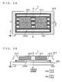
- the differential capacitor 1 may comprise a shield plate 1023 as shown in FIGS. 5A and 5B.
- FIG. 5A is a schematic diagram showing the shield plate 1023 as viewed from vertically above.
- FIG. 5B is a schematic diagram showing a cross section of the shield plate 1023 taken at a vertical plane A-A' in FIG. 5A , as viewed in the direction of arrow C.
- the shield plate 1023 is a plate-like component composed of a conductive material, which has a symmetrical shape with respect to the vertical plane B-B', as is the case with the shield plate 1022.
- the shield plate 1022 is interposed between the semiconductor substrate 1020 and both lower electrodes 1016 and 1018.
- the shield plate 1023 has one or more slits 10231 formed therein.
- the slit(s) 10231 is formed so as to be substantially parallel to the x-axis direction and perpendicular to the aforementioned virtual ground.
- the slit(s) 10231 is formed so that the above-defined optimum overlap ratio is about 70%.
- the slits 10231 are preferably formed so as to extend in parallel to each other along the x-axis direction.
- the slits 10231 maybe formed so as to be parallel to the y-axis direction, in this case any leak component from the differential capacitor 1 would take a long time to arrive at the virtual ground, and propagate through the shield plate 1023 in a substantially spiral manner. As a result, an inductance component occurs in the shield plate 1023, thereby deteriorating the shielding effect.
- the differential capacitor 1 may comprise a shield plate 1024 as shown in FIGS. 6A and 6B.
- FIG. 6A is a schematic diagram showing the shield plate 1024 as viewed from vertically above.
- FIG. 6B is a schematic diagram showing a cross section of the shield plate 1024 taken at a vertical plane A-A' in FIG. 6A , as viewed in the direction of arrow C.
- the shield plate 1024 is preferably a plate-like piece of conductive material which is symmetrical with respect to the vertical plane B-B', as is the case with the shield plate 1022.
- the shield plate 1024 has a substantially rectangular shape, such that each of the two sides extend in parallel to the x-axis direction has a length of Lx.
- a plurality of through-holes 10241 are formed in the shield plate 1024, in such a manner that the above-defined optimum overlap ratio equals about 70% in order to prevent deterioration in both the quality factor and the capacitance variation ratio.
- the through-holes 10241 are arranged so as to be substantially parallel to both the x-axis direction and the y-axis direction.
- Any two adjoining through-holes 10241 along the x-axis direction are disposed apart by a distance ⁇ between their respective centers.
- An in-phase signal and a reverse-phase signal also leak from the differential capacitor 1 to the shield plate 1024.
- standing waves having a wavelength of ⁇ will propagate on the shield plate 1024.
- the standing waves can be prevented from leaking from each through-hole 10241 to the semiconductor substrate 1020. As a result, the deterioration in the quality factor of the differential capacitor 1 can be prevented.
- the through-holes 10241 may be arranged in concentric circles centered around a point on the virtual ground, with a distance of ⁇ between every two adjoining concentric circles.
- the shield plate 1022, 1023, or 1024 may be connected to ground (not shown) via an inductance and/or a resistance, in order to prevent charge accumulation.
- the virtual ground in the shield plate 1022, 1023, or 1024 may directly be electrically connected to ground (not shown) in order to prevent charge accumulation in the shield plate 1022, 1023, or 1024.
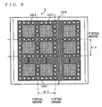
- FIG. 8A is a schematic diagram illustrating a differential capacitor 2 as viewed from vertically above.
- FIG. 8B is a schematic diagram showing a cross section of the differential capacitor 2 taken at a vertical plane A-A' in FIG. 8A , as viewed in the direction of arrow C.
- FIGS. 8A and 8B also show a three-dimensional coordinate system having three orthogonal axes of x, y, and z, where the z axis corresponds to the vertically upward direction, and the x and y axes correspond to the two respectively perpendicular directions on the horizontal plane. Note that the y axis is in the same direction as that of arrow C, and extends in parallel to a vertical plane B-B' described later.
- the differential capacitor 2 comprises first to fourth capacitors 2001 to 2004 and a shield plate 2005.
- the first to fourth capacitors 2001 to 2004 are formed in an interlayer film 1019 on the semiconductor substrate 1020.
- the semiconductor substrate 1020 and the interlayer film 1019 are identical to those described above in the "Description of the Background Art" section.
- the first to fourth capacitors 2001 to 2004 are composed of metal wires which are typically aluminum.
- the first capacitor 2001 includes an upper electrode 2006 and a lower electrode 2007, which are disposed substantially parallel to each other with a predetermined interval along the z-axis direction (along the vertical direction).
- the upper electrode 2006 and the lower electrode 2007 are formed in positions which are away from the vertical plane A-A' (which extends in parallel to the x-axis direction) by a predetermined distance in a plus direction of the y axis, and away from the vertical plane B-B' (which extends in parallel to the ⁇ -axis direction) by a predetermined distance in the minus direction of the x axis.
- the second capacitor 2002 includes an upper electrode 2008 and a lower electrode 2009, which have substantially symmetrical configurations to those of the upper electrode 2006 and the lower electrode 2007, respectively, with respect to the vertical plane B-B'.
- the third capacitor 2003 includes an upper electrode 2010 and a lower electrode 2011 (not explicitly shown) , which have substantially symmetrical configurations to those of the upper electrode 2006 and the lower electrode 2007, respectively, with respect to the vertical plane A-A'.
- the fourth capacitor 2004 includes an upper electrode 2012 and a lower electrode 2013 (not explicitly shown), which have substantially symmetrical configurations to those of the upper electrode 2008 and the lower electrode 2009, respectively, with respect to the vertical plane A-A'.
- the shield plate 2005 is preferably a plate-like piece of conductive material which is symmetrical with respect to the vertical plane A-A' and with respect to the vertical plane B-B' . More specifically, the shield plate 2005 has a substantially square shape, each side having a length of L. The shield plate 2005 is disposed so as to come between the semiconductor substrate 1020 and all of the lower electrode 2007, 2009, 2011, and 2013.
- a plurality of through-holes 20051 are formed in the shield plate 2005. For clarity, only one of the through-holes is labeled as "20051" in FIGS. 8A and 8B .
- the through-holes 2005 are arranged in the x-axis direction and in the ⁇ -axis direction. There are an odd number linear arrays of through-holes 20051 extending in parallel to the y axis and an odd number linear arrays of through-holes 20051 extending in parallel to the x axis (nine such arrays are shown in FIGS. 8A and 8B ) .
- the linear arrays of through-holes 20051 extending in parallel to the y axis will be referred to as "columns", whereas the linear arrays of through-holes 20051 extending in parallel to the x axis will be referred to as "rows".
- the through-holes 20051 are disposed in such a manner that the center of each of the through-holes 20051 composing the central column is on a line at which the shield plate 2005 is intersected by the vertical plane B-B' and that the center of each of the through-holes 20051 composing the central row is on a line at which the shield plate 2005 is intersected by the vertical plane A-A'. Any two adjoining through-holes 20051 along the x-axis direction or the y-axis direction are disposed apart by a distance ⁇ between their respective centers.
- an in-phase signal composing a differential pair of signals is supplied to the first capacitor 2001 and the fourth capacitor 2004, which are formed in point-symmetrical positions from each other with respect to an intersection between the vertical plane A-A', the vertical plane B-B', and the shield plate 2005.
- a reverse-phase signal composing the differential pair of signals is supplied to the second capacitor 2002 and the third capacitor 2003, which are formed in point-symmetrical positions from each other with respect to the aforementioned intersection.
- the distance from each of the two sides of the shield plate 2005 extending in parallel to the y axis to the virtual ground (vertical plane B-B') and the distance from each of the two sides of the shield plate 2005 extending in parallel to the x axis to the virtual ground (vertical plane A-A') is each prescribed to be n ⁇ /2+ ⁇ /4, where n indicates the number of columns and rows (n being an integer which is equal to or greater than zero) .
- ⁇ ⁇ /2.
- the differential capacitor 2 includes two capacitors (along the x-axis direction) by two capacitors (along the y-axis direction)
- the present invention is not limited thereto.
- the differential capacitor 2 may include three or more capacitors (along the x-axis direction) by three or more capacitors (along the y-axis direction) , according to the principle described above. In this case, it is preferable that the distance between any two adjoining virtual grounds along the x axis or the y axis is equal to n ⁇ .
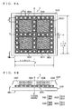
- FIG. 10A is a schematic diagram illustrating a differential capacitor 3 according to a third embodiment as viewed from vertically above.
- FIG. 10B is a schematic diagram showing a cross section of the differential capacitor 3 taken at a vertical plane A-A' in FIG. 10A , as viewed in the direction of arrow C.
- FIGS. 10A and 10B also show a three-dimensional coordinate system having three orthogonal axes of x, y, and z, where the z axis corresponds to the vertically upward direction, and the x and y axes correspond to the two respectively perpendicular directions on the horizontal plane. Note that the y axis is in the same direction as that of arrow C, and extends in parallel to a vertical plane B-B' described later.
- the differential capacitor 3 includes first to fourth capacitors 3001 to 3004 and a shield plate 3005.
- the first to fourth capacitors 3001 to 3004 are formed in the interlayer film 1019 on the semiconductor substrate 1020.
- the semiconductor substrate 1020 and the interlayer film 1019 are identical to those described above in the "Description of the Background Art" section.
- the first to fourth capacitors 3001 to 3004 are composed of metal wires which are typically aluminum.
- the first capacitor 3001 includes a first electrode 3015 and a second electrode 3016.
- the first electrode 3015 is a comb-shaped electrode having a predetermined width w, including combtooth portions which are disposed with a pitch of ⁇ .
- the first electrode 3015 is formed in a position which is away from the vertical plane B-B' (which is parallel to the YZ plane) by a predetermined distance in the minus direction of the x axis.
- the combtooth portions of the first electrode 3015 are oriented so as to intersect the vertical plane A-A'.
- the second electrode 3016 has substantially the same shape as that of the first electrode 3015, although the second electrode 3016 is formed in a different position from the first electrode 3015.
- the second electrode 3016 is formed in a position which is translated by a distance d (where d ⁇ ( ⁇ -w) /2), in the plus direction or the minus direction of the x axis, from a position which is symmetrical from the first electrode 3015 with respect to the vertical plane A-A' .
- d where d ⁇ ( ⁇ -w) /2
- the first electrode 3015 and the second electrode 3016 appear as "engaging each other" when viewed from vertically above. Consequently, fringe capacitances can occur between adjacent combtooth portions of the first electrode 3015 and the second electrode 3016.
- the second capacitor 3002 similarly includes a first electrode 3015 and a second electrode 3016.
- the second capacitor 3002 is formed in a position which is translated by a predetermined distance, in the minus direction of the z axis, from a position which is substantially symmetrical from the first electrode 3015 with respect to the vertical plane A-A'.
- fringe capacitances occur between adjacent combtooth portions along the x-axis direction.
- fringe capacitances can also occur between adjacent combtooth portions, along the z-axis direction, of the first capacitor 3001 and the second capacitor 3002.
- the third capacitor 3003 is formed in a position which is substantially symmetrical from the first capacitor 3001 with respect to the vertical plane B-B'.
- the fourth capacitor 3004 is formed in a position which is substantially symmetrical from the second capacitor 3002 with respect to the vertical plane B-B'.
- fringe capacitances can also occur in the third and fourth capacitors 3003 and 3004, as described above.
- FIG. 11 is a schematic diagram showing an equivalent circuit of the differential capacitor 3 shown in FIGS. 10A and 10B .
- a combtooth portion A1 is the leftmost combtooth portion of the second electrode 3016 of the first capacitor 3001.
- a combtooth portion A2 is a combtooth portion of the second electrode 3016 of the first capacitor 3001 that lies adjacent to the combtooth portion A1.
- a combtooth portion B1 is the leftmost combtooth portion of the first electrode 3015 of the first capacitor 3001.
- a combtooth portion B2 is a combtooth portion of the first electrode 3015 of the first capacitor 3001 that lies adjacent to the combtooth portion B1.
- a combtooth portion B3 is a combtooth portion of the second capacitor 3002 that opposes the combtooth portion A1 along the z-axis direction.
- a combtooth portion B4 is a combtooth portion of the second capacitor 3002 that opposes the combtooth portion A2 along the z-axis direction.
- a combtooth portion A3 is a combtooth portion of the second capacitor 3002 that opposes the combtooth portion B1 along the z-axis direction.
- a combtooth portion A4 is a combtooth portion of the second capacitor 3002 that opposes the combtooth portion B2 along the z-axis direction.
- the combtooth portion A1 When an in-phase signal or a reverse-phase signal of a differential pair of signals is supplied to the first and second capacitors 3001 and 3002 having the above structures, the combtooth portion A1 will have a fringe capacitance C11 between itself and a side face of the combtooth portion B1.
- the combtooth portions A1 and 83 will have a capacitance C13, between the lower face of the combtooth portion A1 and the upper face of the combtooth portion B3.
- fringe capacitances C21, C22, C33, C34, and C44 as shown in FIG. 11 also will occur with respect to the other combtooth portions, and capacitance C31, C14, and C42 will occur.
- a total capacitance value Ctotal occurring among the combtooth portions A1 to A4 and B1 to B4 can be expressed by equation (2) below:
- Ctotal C ⁇ 11 + C ⁇ 13 + C ⁇ 33 + C ⁇ 31 + C ⁇ 21 + C ⁇ 24 + C ⁇ 34 + C ⁇ 22 + C ⁇ 42 + C ⁇ 44
- the shield plate 3005 is a plate-like component composed of a conductive material such as aluminum, which has a symmetrical shape with respect to the vertical plane B-B' along the horizontal direction.
- the shield plate 3005 is interposed between the semiconductor substrate 1020 and both the second capacitor 3002 and the fourth capacitor 3004.
- the shield plate 3005 has a shape such that, when the second capacitor 3002 and the fourth capacitor 3004 are proj ected onto the shield plate 3005 fromvertically above, the projected second capacitor 3002 and fourth capacitor 3004 appear as partially overlapping with the shield plate 3005.
- a portion of each of the second capacitor 3002 and the fourth capacitor 3004 whose projected image overlaps with the shield plate 3005 will be referred to as an "overlapping region Ao".
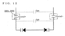
- the parasitic capacitances Cpa and Cpb (shown as dot-line images) as shown in FIG. 12 occur between the upper face of the shield plate 3005 and the lower faces of the combtooth portions A3, A4, B3, and B4.
- the differential capacitor 3 is incorporated in the differential oscillation circuit 7, for example, such parasitic capacitances Cpa and Cpb will affect the oscillation frequency range thereof.
- the differential capacitor 3 and the semiconductor substrate 1020 are coupled together via large parasitic capacitances occurring on both sides of the differential capacitor 3, so that the influence of the parasitic resistances occurring in the semiconductor substrate 1020 becomes outstanding.
- the quality factor of the differential capacitor 3 would be deteriorated, thereby affecting the C/N (Carrier to Noise ratio) of the differential oscillation circuit.
- the overlap ratio may also be optimized in the present embodiment as described in the previous embodiments, thereby minimizing the deterioration in the oscillation frequency range of the differential oscillation circuit 7 and minimizing C/N deterioration in the differential oscillation circuit 7.
- the overlap ratio is defined as (So/S) ⁇ 100 [%], where S is the total area of the lower faces of the second capacitor 3002 and the fourth capacitor 3004, and So is the total area of the overlapping regions Ao in the second capacitor 3002 and the fourth capacitor 3004.
Landscapes
- Physics & Mathematics (AREA)
- Electromagnetism (AREA)
- Semiconductor Integrated Circuits (AREA)
- Inductance-Capacitance Distribution Constants And Capacitance-Resistance Oscillators (AREA)
- Filters And Equalizers (AREA)
Claims (13)
- Oscillateur différentiel (7) ayant un condensateur différentiel (1, 2, 3) comprenant une pluralité de condensateurs (1003 et 1004, 2002 à 2004, ou 3001 à 3004), ayant chacun une électrode supérieure (1015, 1017) et une électrode inférieure (1016, 1018) qui sont parallèles l'une à l'autre le long d'une direction verticale, comprenant en outre au moins un condensateur variable (1005 ou 1006) qui est relié à chaque électrode inférieure (1016, 1018) ou au moins un condensateur variable (1005 ou 1006) qui est relié à chaque électrode supérieure (1015, 1017),
dans lequel,
l'un quelconque de la pluralité de condensateurs (1003 et 1004, 2002 à 2004, ou 3001 à 3004) est formé sur un substrat semi-conducteur (1020) dans une position symétrique à partir de l'autre de la pluralité de condensateurs (1003 et 1004, 2002 à 2004, ou 3001 à 3004) par rapport à un plan vertical (B-B'),
le condensateur différentiel (1, 2, 3) comprend en outre une plaque de blindage (1022 à 1024, 2005 ou 3005) interposée entre chaque électrode inférieure (1016, 1018) et le substrat semi-conducteur (1020),
la plaque de blindage (1022 à 1024, 2005 ou 3005) est reliée à la masse par l'intermédiaire d'une inductance et/ ou d'une résistance, et
lorsque chaque électrode inférieure (1016, 1018) est projetée sur la plaque de blindage (1022 à 1024, 2005 ou 3005) le long de la direction verticale,
caractérisé en ce que
chaque électrode inférieure projetée (1016, 1018) a un chevauchement partiel avec la plaque de blindage (1022 à 1024, 2005 ou 3005),
où le chevauchement partiel de chaque électrode inférieure projetée (1016, 1018) avec la plaque de blindage (1022 à 1024, 2005 ou 3005) est sélectionné pour être supérieur à 0% et inférieur ou égal à 70% d'une zone de l'électrode inférieure (1016, 1018). - Oscillateur différentiel (7) selon la revendication 1, dans lequel chaque électrode inférieure projetée (1016, 1018) s'étend à l'extérieur de la plaque de blindage (1022 à 1024, 2005 ou 3005).
- Oscillateur différentiel (7) selon la revendication 1, dans lequel la plaque de blindage (1023) présente une fente (10231) formée dedans.
- Oscillateur différentiel (7) selon la revendication 3, dans lequel la fente (10 231) coupe le plan vertical (B-B').
- Oscillateur différentiel (7) selon la revendication 1, dans lequel la plaque de blindage (1024) présente une pluralité de trous débouchants (10241, 20051) formés dedans.
- Oscillateur différentiel (7) selon la revendication 5, dans lequel,
la pluralité de trous débouchants (10241, 20051) sont disposés le long de deux directions prédéterminées à des intervalles égaux, et
l'intervalle entre des trous débouchants adjacents de la pluralité de trous débouchants (10241, 20051) est égal à un multiple entier de 1/2 d'une longueur d'onde d'ondes stationnaires qui se propagent à travers la plaque de blindage (1022 à 1024, 2005 ou 3005). - Oscillateur différentiel (7) selon la revendication 6, dans lequel une longueur de deux côtés prédéterminés de la plaque de blindage (1022 à 1024, 2005 ou 3005) au plan vertical (B-B') est égale à une somme d'un multiple entier de 1/2 de la longueur d'onde des ondes stationnaires et 1/4 de la longueur d'onde des ondes stationnaires.
- Oscillateur différentiel (7) selon la revendication 1, dans lequel, parmi la pluralité de condensateurs (1003 et 1004, 2002 à 2004, ou 3001 à 3004), deux condensateurs quelconque (1003 et 1004, 2002 à 2004, ou 3001 à 3004) adjacents entre eux reçoivent respectivement un signal en phase et un signal de phase inverse comprenant une paire différentielle de signaux.
- Oscillateur différentiel (7) selon la revendication 1, dans lequel une partie de la plaque de blindage (1022 à 1024, 2005 ou 3005) qui coupe le plan vertical (B-B') est reliée à la masse.
- Oscillateur différentiel (7) selon la revendication 1, dans lequel la zone de chevauchement partiel de chaque électrode inférieure projetée (1016, 1018) avec la plaque de blindage (1022 à 1024, 2005 ou 3005) est déterminée sur la base d'un taux de variation de capacité du circuit à capacité variable (1005, 1006) et d'un facteur de qualité de chaque condensateur.
- Oscillateur différentiel (7) selon la revendication 1, dans lequel,
un premier condensateur (2002) de la pluralité de condensateurs (1003 et 1004, 2002 à 2004, ou 3001 à 3004) est formé sur le substrat semi-conducteur (1020) dans une position symétrique à partir de l'un de la pluralité de condensateurs (1003 et 1004, 2002 à 2004, ou 3001 à 3004) par rapport au plan vertical (B-B'),
un deuxième condensateur (2003) de la pluralité de condensateurs (1003 et 1004, 2002 à 2004, ou 3001 à 3004) est formé sur le substrat semi-conducteur (1020) dans une position symétrique à partir du condensateur par rapport à un plan vertical supplémentaire qui est perpendiculaire au plan vertical (B-B'), et
un troisième condensateur (2004) de la pluralité de condensateurs (1003 et 1004, 2002 à 2004, ou 3001 à 3004) est formé sur le substrat semi-conducteur (1020) dans une position symétrique à partir du condensateur par rapport à une ligne d'intersection entre le plan vertical (B-B') et l'autre plan vertical. - Oscillateur différentiel (7) selon la revendication 11, dans lequel un signal en phase et un signal de phase inverse composant une paire différentielle de signaux sont fournis à la pluralité de condensateurs (1003 et 1004, 2002 à 2004, ou 3001 à 3004) de telle manière que l'un du signal en phase ou du signal de phase inverse soit fourni au condensateur (2002) et au troisième condensateur (2004) et que l'autre du signal en phase ou du signal de phase inverse soit fourni aux premier (2002) et deuxième (2003) condensateurs.
- Oscillateur différentiel (7) selon la revendication 11, dans lequel,
la plaque de blindage (1022 à 1024, 2005 ou 3005) présente une pluralité de trous débouchants (10241, 20051) formés dedans, les trous débouchants (10241, 20051) étant disposés le long de deux directions prédéterminées à des intervalles égaux, de sorte que l'intervalle entre des trous débouchants adjacents de la pluralité de trous débouchants (10241, 20051) soit sensiblement égal à un multiple entier de 1/2 d'une longueur d'onde d'ondes stationnaires qui se propagent à travers la plaque de blindage (1022 à 1024, 2005 ou 3005), et
la plaque de blindage (1022 à 1024, 2005 ou 3005) présente une forme sensiblement rectangulaire de sorte qu'une longueur de deux côtés prédéterminés de la plaque de blindage (1022 à 1024, 2005 ou 3005) au plan vertical (B-B') et une longueur des deux autres côtés de la plaque de blindage (1022 à 1024, 2005 ou 3005) au plan vertical supplémentaire soient chacune sensiblement égales à une somme d'un multiple entier de 1/2 de la longueur d'onde des ondes stationnaires et 1/4 de la longueur d'onde des ondes stationnaires.
Applications Claiming Priority (2)
| Application Number | Priority Date | Filing Date | Title |
|---|---|---|---|
| JP2003191267 | 2003-07-03 | ||
| JP2003191267 | 2003-07-03 |
Publications (3)
| Publication Number | Publication Date |
|---|---|
| EP1496528A2 EP1496528A2 (fr) | 2005-01-12 |
| EP1496528A3 EP1496528A3 (fr) | 2009-07-22 |
| EP1496528B1 true EP1496528B1 (fr) | 2012-09-05 |
Family
ID=33447963
Family Applications (1)
| Application Number | Title | Priority Date | Filing Date |
|---|---|---|---|
| EP04015456A Expired - Lifetime EP1496528B1 (fr) | 2003-07-03 | 2004-07-01 | Oscillateur différentiel |
Country Status (3)
| Country | Link |
|---|---|
| US (1) | US6940707B2 (fr) |
| EP (1) | EP1496528B1 (fr) |
| CN (1) | CN100426505C (fr) |
Families Citing this family (13)
| Publication number | Priority date | Publication date | Assignee | Title |
|---|---|---|---|---|
| US7336475B2 (en) * | 2006-02-22 | 2008-02-26 | Vishay Vitramon, Inc. | High voltage capacitors |
| US8238075B2 (en) * | 2006-02-22 | 2012-08-07 | Vishay Sprague, Inc. | High voltage capacitors |
| EP2247208A4 (fr) * | 2008-02-26 | 2013-10-02 | Softspikes Llc | Crampon de traction amélioré pour sports de plein air |
| WO2011033659A1 (fr) * | 2009-09-18 | 2011-03-24 | 株式会社 東芝 | Dispositif sans fil |
| US9054069B2 (en) * | 2013-09-05 | 2015-06-09 | International Business Machines Corporation | Variable capacitance integrated circuit |
| TWI500934B (zh) * | 2013-09-11 | 2015-09-21 | Pixart Imaging Inc | 具有對稱差分電容的微機電元件 |
| US9739816B2 (en) * | 2013-11-27 | 2017-08-22 | Analog Devices, Inc. | Capacitive sensor with differential shield |
| CN105338399A (zh) * | 2015-10-29 | 2016-02-17 | 小米科技有限责任公司 | 图像获取方法及装置 |
| IL253252B (en) * | 2016-07-28 | 2021-05-31 | Neteera Tech Ltd | Terahertz cmos sensor |
| CN110323334B (zh) * | 2019-07-09 | 2023-03-24 | 四川中微芯成科技有限公司 | 一种用寄生电容做adc电容的结构及方法 |
| US12274244B2 (en) * | 2022-12-28 | 2025-04-15 | Industrial Technology Research Institute | Physiological information sensing device and method |
| CN115931185B (zh) * | 2023-01-03 | 2024-06-11 | 歌尔微电子股份有限公司 | 一种电容式微机电传感器 |
| CN116632001B (zh) * | 2023-07-24 | 2023-10-13 | 合肥晶合集成电路股份有限公司 | 一种半导体装置及半导体装置的设计辅助装置 |
Citations (1)
| Publication number | Priority date | Publication date | Assignee | Title |
|---|---|---|---|---|
| JP2005159280A (ja) * | 2003-07-03 | 2005-06-16 | Matsushita Electric Ind Co Ltd | 差動容量素子、差動アンテナ素子及び差動共振素子 |
Family Cites Families (20)
| Publication number | Priority date | Publication date | Assignee | Title |
|---|---|---|---|---|
| US201846A (en) * | 1878-03-26 | Improvement in beer-pumps | ||
| US171115A (en) * | 1875-12-14 | Improvement in millstones | ||
| US5220483A (en) | 1992-01-16 | 1993-06-15 | Crystal Semiconductor | Tri-level capacitor structure in switched-capacitor filter |
| JP2980142B2 (ja) | 1992-12-10 | 1999-11-22 | 富士通株式会社 | 半導体容量素子およびこれを用いた回路 |
| US5760456A (en) * | 1995-12-21 | 1998-06-02 | Grzegorek; Andrew Z. | Integrated circuit compatible planar inductors with increased Q |
| JP2000500240A (ja) * | 1996-08-29 | 2000-01-11 | フィリップス エレクトロニクス ネムローゼ フェンノートシャップ | 周波数−非依存分圧器 |
| US6366443B1 (en) * | 1997-12-09 | 2002-04-02 | Daniel Devoe | Ceramic chip capacitor of conventional volume and external form having increased capacitance from use of closely-spaced interior conductive planes reliably connecting to positionally-tolerant exterior pads through multiple redundant vias |
| US6066537A (en) * | 1998-02-02 | 2000-05-23 | Tritech Microelectronics, Ltd. | Method for fabricating a shielded multilevel integrated circuit capacitor |
| US6097195A (en) * | 1998-06-02 | 2000-08-01 | Lucent Technologies Inc. | Methods and apparatus for increasing metal density in an integrated circuit while also reducing parasitic capacitance |
| JP2000251379A (ja) * | 1999-02-24 | 2000-09-14 | Mitsumi Electric Co Ltd | 大容量磁気ディスク装置 |
| JP3398693B2 (ja) * | 1999-08-24 | 2003-04-21 | エヌイーシーマイクロシステム株式会社 | 半導体記憶装置 |
| US6489663B2 (en) * | 2001-01-02 | 2002-12-03 | International Business Machines Corporation | Spiral inductor semiconducting device with grounding strips and conducting vias |
| US6903459B2 (en) * | 2001-05-17 | 2005-06-07 | Matsushita Electric Industrial Co., Ltd. | High frequency semiconductor device |
| JP4047064B2 (ja) | 2001-05-17 | 2008-02-13 | 松下電器産業株式会社 | 高周波半導体装置 |
| US6456481B1 (en) * | 2001-05-31 | 2002-09-24 | Greatbatch-Sierra, Inc. | Integrated EMI filter-DC blocking capacitor |
| JP3977053B2 (ja) * | 2001-10-30 | 2007-09-19 | 富士通株式会社 | 容量素子及びその製造方法 |
| JP3842111B2 (ja) * | 2001-11-13 | 2006-11-08 | 富士通株式会社 | 半導体装置及びその製造方法 |
| JP2003188338A (ja) * | 2001-12-13 | 2003-07-04 | Sony Corp | 回路基板装置及びその製造方法 |
| JP3748556B2 (ja) | 2002-03-15 | 2006-02-22 | 松下電器産業株式会社 | 平衡型高周波デバイス |
| CN1292533C (zh) | 2002-03-15 | 2006-12-27 | 松下电器产业株式会社 | 平衡高频器件,平衡特性的改进方法和采用此类器件的平衡高频电路 |
-
2004
- 2004-07-01 EP EP04015456A patent/EP1496528B1/fr not_active Expired - Lifetime
- 2004-07-01 US US10/880,531 patent/US6940707B2/en not_active Expired - Lifetime
- 2004-07-05 CN CNB200410062884XA patent/CN100426505C/zh not_active Expired - Fee Related
Patent Citations (1)
| Publication number | Priority date | Publication date | Assignee | Title |
|---|---|---|---|---|
| JP2005159280A (ja) * | 2003-07-03 | 2005-06-16 | Matsushita Electric Ind Co Ltd | 差動容量素子、差動アンテナ素子及び差動共振素子 |
Also Published As
| Publication number | Publication date |
|---|---|
| US20050002149A1 (en) | 2005-01-06 |
| US6940707B2 (en) | 2005-09-06 |
| CN1577857A (zh) | 2005-02-09 |
| EP1496528A2 (fr) | 2005-01-12 |
| CN100426505C (zh) | 2008-10-15 |
| EP1496528A3 (fr) | 2009-07-22 |
Similar Documents
| Publication | Publication Date | Title |
|---|---|---|
| EP1496528B1 (fr) | Oscillateur différentiel | |
| US6331930B1 (en) | Multilayer capacitor, electronic device and high frequency circuit using the same | |
| US6226169B1 (en) | Multilayer capacitor | |
| US7675729B2 (en) | Internally shielded energy conditioner | |
| US5023578A (en) | Filter array having a plurality of capacitance elements | |
| EP0917165B1 (fr) | Condensateur multicouche | |
| CN101461060B (zh) | 改良的指状叉合金属-绝缘体-金属电容器和其电容器数组 | |
| US6266228B1 (en) | Multilayer capacitor | |
| US9362052B2 (en) | Electronic devices with floating metal rings | |
| FI113583B (fi) | Dielektrinen resonaattori ja menetelmä sen valmistamiseksi | |
| JPH11214256A (ja) | 積層3端子コンデンサアレイ | |
| US4894629A (en) | Bandpass filter having magnetically coupled resonators | |
| US7471137B2 (en) | Frequency-independent voltage divider | |
| US12323129B2 (en) | Resonator and filter | |
| US8860531B2 (en) | Filter having electrical circuit arrangement with concentrated elements in multi-layer substrates | |
| US4208641A (en) | Hybrid integrated impedance converter circuit | |
| US6636108B2 (en) | Filter circuit and electronic device using the same | |
| US7030443B2 (en) | MIM capacitor | |
| JP4933036B2 (ja) | 差動容量素子、差動アンテナ素子及び差動共振素子 | |
| JP3547008B2 (ja) | 集積回路装置 | |
| US20060091443A1 (en) | Composite capacitor | |
| EP0874456A1 (fr) | Résonateur piézoélectrique et composant électronique utilisant un tel résonateur | |
| JP4013734B2 (ja) | Mim容量 | |
| US20250293656A1 (en) | Filter circuit | |
| US20040207041A1 (en) | Capacitor arrangement and method for producing such a capacitor arrangement |
Legal Events
| Date | Code | Title | Description |
|---|---|---|---|
| PUAI | Public reference made under article 153(3) epc to a published international application that has entered the european phase |
Free format text: ORIGINAL CODE: 0009012 |
|
| AK | Designated contracting states |
Kind code of ref document: A2 Designated state(s): AT BE BG CH CY CZ DE DK EE ES FI FR GB GR HU IE IT LI LU MC NL PL PT RO SE SI SK TR |
|
| AX | Request for extension of the european patent |
Extension state: AL HR LT LV MK |
|
| RIN1 | Information on inventor provided before grant (corrected) |
Inventor name: ADACHI, HISASHI Inventor name: NAKATANI, TOSHIFUMI Inventor name: NAKANISHI, KAYO,6-1-35, KOAZA HORIJIRI |
|
| RAP1 | Party data changed (applicant data changed or rights of an application transferred) |
Owner name: PANASONIC CORPORATION |
|
| RIC1 | Information provided on ipc code assigned before grant |
Ipc: H01L 23/522 20060101ALI20090320BHEP Ipc: H01P 7/08 20060101ALI20090320BHEP Ipc: H01Q 9/06 20060101ALI20090320BHEP Ipc: H01Q 9/04 20060101ALI20090320BHEP Ipc: H01L 23/64 20060101AFI20090320BHEP |
|
| PUAL | Search report despatched |
Free format text: ORIGINAL CODE: 0009013 |
|
| AK | Designated contracting states |
Kind code of ref document: A3 Designated state(s): AT BE BG CH CY CZ DE DK EE ES FI FR GB GR HU IE IT LI LU MC NL PL PT RO SE SI SK TR |
|
| AX | Request for extension of the european patent |
Extension state: AL HR LT LV MK |
|
| 17P | Request for examination filed |
Effective date: 20091028 |
|
| AKX | Designation fees paid |
Designated state(s): AT BE BG CH CY CZ DE DK EE ES FI FR GB GR HU IE IT LI LU MC NL PL PT RO SE SI SK TR |
|
| 17Q | First examination report despatched |
Effective date: 20100709 |
|
| GRAP | Despatch of communication of intention to grant a patent |
Free format text: ORIGINAL CODE: EPIDOSNIGR1 |
|
| GRAS | Grant fee paid |
Free format text: ORIGINAL CODE: EPIDOSNIGR3 |
|
| GRAA | (expected) grant |
Free format text: ORIGINAL CODE: 0009210 |
|
| RIN1 | Information on inventor provided before grant (corrected) |
Inventor name: NAKANISHI, KAYO Inventor name: NAKATANI, TOSHIFUMI Inventor name: ADACHI, HISASHI |
|
| AK | Designated contracting states |
Kind code of ref document: B1 Designated state(s): AT BE BG CH CY CZ DE DK EE ES FI FR GB GR HU IE IT LI LU MC NL PL PT RO SE SI SK TR |
|
| REG | Reference to a national code |
Ref country code: GB Ref legal event code: FG4D |
|
| REG | Reference to a national code |
Ref country code: CH Ref legal event code: EP |
|
| REG | Reference to a national code |
Ref country code: AT Ref legal event code: REF Ref document number: 574461 Country of ref document: AT Kind code of ref document: T Effective date: 20120915 |
|
| REG | Reference to a national code |
Ref country code: IE Ref legal event code: FG4D |
|
| REG | Reference to a national code |
Ref country code: DE Ref legal event code: R096 Ref document number: 602004039188 Country of ref document: DE Effective date: 20121031 |
|
| REG | Reference to a national code |
Ref country code: AT Ref legal event code: MK05 Ref document number: 574461 Country of ref document: AT Kind code of ref document: T Effective date: 20120905 |
|
| REG | Reference to a national code |
Ref country code: NL Ref legal event code: VDEP Effective date: 20120905 |
|
| PG25 | Lapsed in a contracting state [announced via postgrant information from national office to epo] |
Ref country code: AT Free format text: LAPSE BECAUSE OF FAILURE TO SUBMIT A TRANSLATION OF THE DESCRIPTION OR TO PAY THE FEE WITHIN THE PRESCRIBED TIME-LIMIT Effective date: 20120905 Ref country code: CY Free format text: LAPSE BECAUSE OF FAILURE TO SUBMIT A TRANSLATION OF THE DESCRIPTION OR TO PAY THE FEE WITHIN THE PRESCRIBED TIME-LIMIT Effective date: 20120905 Ref country code: FI Free format text: LAPSE BECAUSE OF FAILURE TO SUBMIT A TRANSLATION OF THE DESCRIPTION OR TO PAY THE FEE WITHIN THE PRESCRIBED TIME-LIMIT Effective date: 20120905 |
|
| PG25 | Lapsed in a contracting state [announced via postgrant information from national office to epo] |
Ref country code: SE Free format text: LAPSE BECAUSE OF FAILURE TO SUBMIT A TRANSLATION OF THE DESCRIPTION OR TO PAY THE FEE WITHIN THE PRESCRIBED TIME-LIMIT Effective date: 20120905 Ref country code: GR Free format text: LAPSE BECAUSE OF FAILURE TO SUBMIT A TRANSLATION OF THE DESCRIPTION OR TO PAY THE FEE WITHIN THE PRESCRIBED TIME-LIMIT Effective date: 20121206 Ref country code: SI Free format text: LAPSE BECAUSE OF FAILURE TO SUBMIT A TRANSLATION OF THE DESCRIPTION OR TO PAY THE FEE WITHIN THE PRESCRIBED TIME-LIMIT Effective date: 20120905 |
|
| PG25 | Lapsed in a contracting state [announced via postgrant information from national office to epo] |
Ref country code: EE Free format text: LAPSE BECAUSE OF FAILURE TO SUBMIT A TRANSLATION OF THE DESCRIPTION OR TO PAY THE FEE WITHIN THE PRESCRIBED TIME-LIMIT Effective date: 20120905 Ref country code: ES Free format text: LAPSE BECAUSE OF FAILURE TO SUBMIT A TRANSLATION OF THE DESCRIPTION OR TO PAY THE FEE WITHIN THE PRESCRIBED TIME-LIMIT Effective date: 20121216 Ref country code: BE Free format text: LAPSE BECAUSE OF FAILURE TO SUBMIT A TRANSLATION OF THE DESCRIPTION OR TO PAY THE FEE WITHIN THE PRESCRIBED TIME-LIMIT Effective date: 20120905 Ref country code: NL Free format text: LAPSE BECAUSE OF FAILURE TO SUBMIT A TRANSLATION OF THE DESCRIPTION OR TO PAY THE FEE WITHIN THE PRESCRIBED TIME-LIMIT Effective date: 20120905 Ref country code: RO Free format text: LAPSE BECAUSE OF FAILURE TO SUBMIT A TRANSLATION OF THE DESCRIPTION OR TO PAY THE FEE WITHIN THE PRESCRIBED TIME-LIMIT Effective date: 20120905 Ref country code: CZ Free format text: LAPSE BECAUSE OF FAILURE TO SUBMIT A TRANSLATION OF THE DESCRIPTION OR TO PAY THE FEE WITHIN THE PRESCRIBED TIME-LIMIT Effective date: 20120905 |
|
| PG25 | Lapsed in a contracting state [announced via postgrant information from national office to epo] |
Ref country code: PL Free format text: LAPSE BECAUSE OF FAILURE TO SUBMIT A TRANSLATION OF THE DESCRIPTION OR TO PAY THE FEE WITHIN THE PRESCRIBED TIME-LIMIT Effective date: 20120905 Ref country code: SK Free format text: LAPSE BECAUSE OF FAILURE TO SUBMIT A TRANSLATION OF THE DESCRIPTION OR TO PAY THE FEE WITHIN THE PRESCRIBED TIME-LIMIT Effective date: 20120905 Ref country code: PT Free format text: LAPSE BECAUSE OF FAILURE TO SUBMIT A TRANSLATION OF THE DESCRIPTION OR TO PAY THE FEE WITHIN THE PRESCRIBED TIME-LIMIT Effective date: 20130107 |
|
| PLBE | No opposition filed within time limit |
Free format text: ORIGINAL CODE: 0009261 |
|
| STAA | Information on the status of an ep patent application or granted ep patent |
Free format text: STATUS: NO OPPOSITION FILED WITHIN TIME LIMIT |
|
| PG25 | Lapsed in a contracting state [announced via postgrant information from national office to epo] |
Ref country code: DK Free format text: LAPSE BECAUSE OF FAILURE TO SUBMIT A TRANSLATION OF THE DESCRIPTION OR TO PAY THE FEE WITHIN THE PRESCRIBED TIME-LIMIT Effective date: 20120905 Ref country code: BG Free format text: LAPSE BECAUSE OF FAILURE TO SUBMIT A TRANSLATION OF THE DESCRIPTION OR TO PAY THE FEE WITHIN THE PRESCRIBED TIME-LIMIT Effective date: 20121205 |
|
| 26N | No opposition filed |
Effective date: 20130606 |
|
| PG25 | Lapsed in a contracting state [announced via postgrant information from national office to epo] |
Ref country code: IT Free format text: LAPSE BECAUSE OF FAILURE TO SUBMIT A TRANSLATION OF THE DESCRIPTION OR TO PAY THE FEE WITHIN THE PRESCRIBED TIME-LIMIT Effective date: 20120905 |
|
| REG | Reference to a national code |
Ref country code: DE Ref legal event code: R097 Ref document number: 602004039188 Country of ref document: DE Effective date: 20130606 |
|
| PG25 | Lapsed in a contracting state [announced via postgrant information from national office to epo] |
Ref country code: MC Free format text: LAPSE BECAUSE OF FAILURE TO SUBMIT A TRANSLATION OF THE DESCRIPTION OR TO PAY THE FEE WITHIN THE PRESCRIBED TIME-LIMIT Effective date: 20120905 |
|
| REG | Reference to a national code |
Ref country code: CH Ref legal event code: PL |
|
| REG | Reference to a national code |
Ref country code: IE Ref legal event code: MM4A |
|
| PG25 | Lapsed in a contracting state [announced via postgrant information from national office to epo] |
Ref country code: CH Free format text: LAPSE BECAUSE OF NON-PAYMENT OF DUE FEES Effective date: 20130731 Ref country code: LI Free format text: LAPSE BECAUSE OF NON-PAYMENT OF DUE FEES Effective date: 20130731 |
|
| PG25 | Lapsed in a contracting state [announced via postgrant information from national office to epo] |
Ref country code: IE Free format text: LAPSE BECAUSE OF NON-PAYMENT OF DUE FEES Effective date: 20130701 |
|
| PG25 | Lapsed in a contracting state [announced via postgrant information from national office to epo] |
Ref country code: TR Free format text: LAPSE BECAUSE OF FAILURE TO SUBMIT A TRANSLATION OF THE DESCRIPTION OR TO PAY THE FEE WITHIN THE PRESCRIBED TIME-LIMIT Effective date: 20120905 |
|
| PG25 | Lapsed in a contracting state [announced via postgrant information from national office to epo] |
Ref country code: LU Free format text: LAPSE BECAUSE OF NON-PAYMENT OF DUE FEES Effective date: 20130701 Ref country code: HU Free format text: LAPSE BECAUSE OF FAILURE TO SUBMIT A TRANSLATION OF THE DESCRIPTION OR TO PAY THE FEE WITHIN THE PRESCRIBED TIME-LIMIT; INVALID AB INITIO Effective date: 20040701 |
|
| REG | Reference to a national code |
Ref country code: FR Ref legal event code: PLFP Year of fee payment: 13 |
|
| REG | Reference to a national code |
Ref country code: FR Ref legal event code: PLFP Year of fee payment: 14 |
|
| REG | Reference to a national code |
Ref country code: FR Ref legal event code: PLFP Year of fee payment: 15 |
|
| PGFP | Annual fee paid to national office [announced via postgrant information from national office to epo] |
Ref country code: DE Payment date: 20190719 Year of fee payment: 16 Ref country code: FR Payment date: 20190719 Year of fee payment: 16 |
|
| PGFP | Annual fee paid to national office [announced via postgrant information from national office to epo] |
Ref country code: GB Payment date: 20190719 Year of fee payment: 16 |
|
| REG | Reference to a national code |
Ref country code: DE Ref legal event code: R119 Ref document number: 602004039188 Country of ref document: DE |
|
| GBPC | Gb: european patent ceased through non-payment of renewal fee |
Effective date: 20200701 |
|
| PG25 | Lapsed in a contracting state [announced via postgrant information from national office to epo] |
Ref country code: GB Free format text: LAPSE BECAUSE OF NON-PAYMENT OF DUE FEES Effective date: 20200701 Ref country code: FR Free format text: LAPSE BECAUSE OF NON-PAYMENT OF DUE FEES Effective date: 20200731 |
|
| PG25 | Lapsed in a contracting state [announced via postgrant information from national office to epo] |
Ref country code: DE Free format text: LAPSE BECAUSE OF NON-PAYMENT OF DUE FEES Effective date: 20210202 |