EP1496549B1 - Diode de redressement et de protection - Google Patents
Diode de redressement et de protection Download PDFInfo
- Publication number
- EP1496549B1 EP1496549B1 EP04103289A EP04103289A EP1496549B1 EP 1496549 B1 EP1496549 B1 EP 1496549B1 EP 04103289 A EP04103289 A EP 04103289A EP 04103289 A EP04103289 A EP 04103289A EP 1496549 B1 EP1496549 B1 EP 1496549B1
- Authority
- EP
- European Patent Office
- Prior art keywords
- layer
- substrate
- diode
- doped
- type
- Prior art date
- Legal status (The legal status is an assumption and is not a legal conclusion. Google has not performed a legal analysis and makes no representation as to the accuracy of the status listed.)
- Expired - Lifetime
Links
Images

Classifications
-
- H—ELECTRICITY
- H10—SEMICONDUCTOR DEVICES; ELECTRIC SOLID-STATE DEVICES NOT OTHERWISE PROVIDED FOR
- H10D—INORGANIC ELECTRIC SEMICONDUCTOR DEVICES
- H10D8/00—Diodes
- H10D8/411—PN diodes having planar bodies
-
- H—ELECTRICITY
- H10—SEMICONDUCTOR DEVICES; ELECTRIC SOLID-STATE DEVICES NOT OTHERWISE PROVIDED FOR
- H10D—INORGANIC ELECTRIC SEMICONDUCTOR DEVICES
- H10D8/00—Diodes
- H10D8/60—Schottky-barrier diodes
-
- H—ELECTRICITY
- H10—SEMICONDUCTOR DEVICES; ELECTRIC SOLID-STATE DEVICES NOT OTHERWISE PROVIDED FOR
- H10D—INORGANIC ELECTRIC SEMICONDUCTOR DEVICES
- H10D84/00—Integrated devices formed in or on semiconductor substrates that comprise only semiconducting layers, e.g. on Si wafers or on GaAs-on-Si wafers
- H10D84/201—Integrated devices formed in or on semiconductor substrates that comprise only semiconducting layers, e.g. on Si wafers or on GaAs-on-Si wafers characterised by the integration of only components covered by H10D1/00 or H10D8/00, e.g. RLC circuits
- H10D84/204—Integrated devices formed in or on semiconductor substrates that comprise only semiconducting layers, e.g. on Si wafers or on GaAs-on-Si wafers characterised by the integration of only components covered by H10D1/00 or H10D8/00, e.g. RLC circuits of combinations of diodes or capacitors or resistors
- H10D84/221—Integrated devices formed in or on semiconductor substrates that comprise only semiconducting layers, e.g. on Si wafers or on GaAs-on-Si wafers characterised by the integration of only components covered by H10D1/00 or H10D8/00, e.g. RLC circuits of combinations of diodes or capacitors or resistors of only diodes
Definitions
- the present invention relates to the field of vertical diodes intended for rectification and / or protection used, for example, in power supplies of portable devices such as cameras, cameras, electronic diaries, wireless and / or mobile telephones. or even laptops.
- Schottky diodes or PN junction diodes are used.
- the Figure 1A illustrates, in partial and schematic sectional view, a vertical power diode Schottky type.
- the Schottky diode is formed in a lightly doped semiconductor layer 1 of a first conductivity type, generally N.
- the layer 1 rests on a more strongly doped N-type substrate 2 than the layer 1.
- the substrate 2 is covered on the rear face cathode metallization (not shown).
- the layer 1 is partially covered with a thin layer 3 of a material suitable for forming a Schottky junction with the layer 1.
- the layer 3 is integral with an anode metallization 4.
- the diode generally comprises a guard ring 6 formed by diffusion on the front face on the surface of the layer 1. It will be noted that this guard ring 6 can be considered as forming a PN diode with the layer 1, but that this PN diode is not optimized for a protection function.
- the Figure 1B illustrates the shape of the I (V) characteristic of a Schottky diode.
- a Schottky diode has a low direct voltage drop V F , generally less than 0.5 V, even for large currents, that is to say above 1 A.
- V F direct voltage drop
- a Schottky diode exhibits bad behavior. in inverse polarization, that is to say that the avalanche is not very clear and that the curve I (V) in inverse has a low slope, which causes that the voltage drop across the diode greatly increases when the reverse current flowing through it increases.
- the Figure 2A is a schematic sectional view of a vertical PN diode for providing a protection function.
- the diode is formed in an N type doped semiconductor substrate 11.
- the diode comprises a strongly doped (N + ) N layer coated with a cathode metallization (not shown).
- the substrate 11 On the front face, the substrate 11 comprises a P-type lightly doped region 12 generally surrounded by a very heavily P-type annular region 13. Part of the region 12 is integral with an anode metallization 14.
- a PN diode presents in reverse bias an avalanche behavior satisfying, that beyond an avalanche voltage V BR the slope of the curve I (V) is very high.
- the component 10 has a relatively high voltage drop and varies with the current.
- the doping of the substrate 11 is currently of the order of 10 17 to 10 18 at.cm -3 to optimize the reverse breakdown characteristic.
- Schottky type diodes are preferably used.
- the protection function that is to say, obtaining a voltage Conversely substantially constant, is essential, it is preferred to use PN type diodes.
- the present invention aims at providing a vertical diode which has both a low direct voltage drop and a steep reverse-polarized characteristic.
- the present invention also aims at providing a method for forming such a diode.
- the present invention provides a vertical power, rectification and protection diode, formed in a lightly doped semiconductor layer of a first conductivity type, resting on a heavily doped substrate of the first conductivity type, comprising a first annular region, of the first type of conductivity more heavily doped than said layer and more weakly than said substrate, surrounding an area of said layer and extending to the substrate; and a second annular region, doped with the second type of conductivity, extending on the surface of the first region and on either side thereof; a first electrode having a thin layer of a material adapted to form a Schottky junction with said layer, resting on said zone of said layer and on at least a portion of the second annular region with which it forms an ohmic contact.
- the first type of conductivity is the N type and the second type is the P type.
- the present invention also provides a method of forming a vertical diode on a highly doped monocrystalline silicon substrate of a first conductivity type, comprising the steps of forming on the substrate a lower doped semiconductor layer of the first conductivity type. that the substrate; forming, in said layer, a first annular region extending to the substrate, the first annular region being doped with the first conductivity type more strongly than said layer and more weakly than said substrate; forming a second annular region, doped with the second conductivity type, extending on the surface of the first region and on either side thereof at the surface of the layer and the zone; and depositing, on said zone of said layer and on a portion of the second annular region, a thin layer of a material suitable for forming a Schottky junction with said layer.
- the method further comprises the steps of forming, on the rear face, a metallization on at least a portion of the substrate and, on the front face, another metallization on at least a portion of the thin layer.
- FIGS. 3A to 3D illustrate, in a partial and schematic sectional view, steps of a method of forming a vertical power diode according to an embodiment of the present invention.
- the method according to the invention begins with the epitaxial growth, on a monocrystalline silicon substrate 31 of a semiconductor layer 32.
- the substrate 31 is heavily doped N-type, while the layer 32 is slightly doped N-type.
- annular aperture mask 33 is deposited through which implantation of an N type dopant such as phosphorus is performed.
- a zone A surrounded by an annular region 35 is thus delimited in the layer 32.
- the implantation and diffusion annealing conditions are chosen so that the annular region 35 passes through the entire layer 32 and reaches the substrate 31.
- ring 35 is N-doped more strongly than zone A (layer 32) but weaker than substrate 31.
- the mask 33 is removed and replaced by a mask 37 having a annular opening of dimensions greater than those of the mask 33, around the first annular region 35. Then is formed by implantation / diffusion a second annular region 39 of the P type.
- the second region 39 covers the upper surface of the annular region 35 and extends on both sides of it, inwards and outwards. It should be noted that the portion of the second region 39 extending outside the first region 35 results from a diffusion deeper than the central portion, which reinforces the fact that the active PN junction is the junction to the interface between layers 35 and 39.
- the part of the mask 37 protecting the upper surface of the area A is removed and an additional mask 41 is formed for extending the mask 37 over an outer part of the annular region 35 inwards. forms in the space cleared by the mask 37-41 a thin layer 44 adapted to form a Schottky junction with the zone A.
- the layer 44 covers the central and inner portions of the annular region 39 with which it forms an ohmic contact.
- a metallization 46 is formed on the layer 44 intended to form the anode of the rectification and protection diode according to the invention.
- the method according to the invention is continued by usual steps of forming a component, in particular the formation on the rear face of the substrate 31 of a metallization intended to form another electrode, here the cathode, of the diode according to the invention .
- a diode consisting of a central Schottky junction 44-A in parallel with a peripheral PN junction 39-35 is thus obtained.
- the structure according to the invention advantageously makes it possible to reconcile the divergent doping constraints of the Schottky and PN diodes.
- the figure 4 illustrates the characteristic I (V) of a diode according to the present invention, for example of a structure similar to that of the 3D figure .
- the diode according to the present invention behaves like a diode Schottky 38-A and has a relatively low voltage drop which depends on the doping level of the zone A and the Schottky metal used.
- the diode behaves like a PN 39-35 junction and exhibits a steep avalanche behavior which is essentially dependent on the doping of the first annular region 35.
- the doping of the area A (layer 32) and the first annular region 35 may advantageously be independently optimized to minimize the forward voltage drop and maximize reverse voltage resistance while reducing reverse currents (reverse power consumption), respectively.
- a power diode which has a reverse voltage at 1 mA of the order of 16 V and a reverse voltage at an ampere of about 20 V, and a direct voltage drop at a voltage of ampere of the order of 400 mV.
- the inverse characteristics of the PN diode are chosen so that, inversely, it is this PN diode which determines the characteristics of the diode according to the present invention.
- the present invention is susceptible of various variants and modifications which will appear to man art.
- those skilled in the art will be able to adjust the doping levels and the depths of the different regions to the desired performances.
- the diode is formed in a layer 32 resting on a substrate 31.
- the layer 32 could result from uniform doping of a semiconductor wafer and the substrate 31 could result from an epitaxy and / or a specific implantation of the rear face of the wafer.
Landscapes
- Electrodes Of Semiconductors (AREA)
Description
- La présente invention concerne le domaine des diodes verticales destinées au redressement et/ou à la protection utilisées, par exemple, dans des alimentations de dispositifs portables tels que des appareils photographiques, des caméras, des agendas électroniques, des téléphones sans fils et/ou mobiles ou encore des ordinateurs portables.
- Dans de telles applications, on utilise notamment des diodes Schottky ou des diodes à jonction PN.
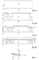
- La
figure 1A illustre, en vue en coupe partielle et schématique, une diode de puissance verticale de type Schottky. La diode Schottky est formée dans une couche semiconductrice 1 faiblement dopée d'un premier type de conductivité, généralement N. La couche 1 repose sur un substrat 2 plus fortement dopé de type N que la couche 1. Le substrat 2 est recouvert en face arrière d'une métallisation de cathode (non représentée). En face avant, la couche 1 est partiellement recouverte d'une couche mince 3 d'un matériau propre à former une jonction Schottky avec la couche 1. La couche 3 est solidaire d'une métallisation d'anode 4. La diode comporte généralement un anneau de garde 6 formé par diffusion en face avant à la surface de la couche 1. On notera que cet anneau de garde 6 peut être considéré comme formant une diode PN avec la couche 1, mais que cette diode PN n'est pas optimisée pour une fonction de protection. - La
figure 1B illustre l'allure de la caractéristique I(V) d'une diode Schottky. Une diode Schottky présente une chute de tension en direct VF faible, généralement inférieure à 0,5 V, même pour des courants importants, c'est-à-dire supérieurs à 1 A. Par contre, une diode Schottky présente un mauvais comportement en polarisation inverse, c'est-à-dire que l'avalanche est peu nette et que la courbe I(V) en inverse a une pente peu élevée, ce qui entraîne que la chute de tension aux bornes de la diode augmente fortement quand le courant inverse qui la traverse augmente. - La
figure 2A est une vue en coupe schématique d'une diode PN verticale destinée à assurer une fonction de protection. La diode est formée dans un substrat semiconducteur 11 dopé de type N. En face arrière, la diode comprend une couche N fortement dopée (N+) revêtue d'une métallisation de cathode (non représentée). En face avant, le substrat 11 comporte une région 12 faiblement dopée de type P généralement entourée d'une région annulaire 13 très fortement dopée de type P. Une partie de la région 12 est solidaire d'une métallisation d'anode 14. - Comme l'illustre la
figure 2B , une diode PN présente en polarisation inverse un comportement en avalanche satisfaisant à savoir qu'au delà d'une tension d'avalanche VBR la pente de la courbe I(V) est très élevée. Toutefois, en polarisation directe, le composant 10 présente une chute de tension relativement élevée et qui varie avec le courant. Le dopage du substrat 11 est couramment de l'ordre de 1017 à 1018 at.cm-3 pour optimiser la caractéristique de claquage en inverse. - Ainsi, dans des applications où la fonction de redressement, c'est-à-dire l'obtention d'une faible chute de tension en direct, est essentielle, on utilise de préférence des diodes de type Schottky. Par contre, dans des applications où la fonction de protection, c'est-à-dire l'obtention d'une tension inverse sensiblement constante, est essentielle, on utilise de préférence des diodes de type PN.
- Toutefois, dans de nombreuses applications parmi lesquelles des convertisseurs d'alimentation et/ou la protection d'alimentation ou de charges dans des dispositifs portables, il est souhaitable d'optimiser à la fois la fonction de redressement et la fonction de protection. La seule façon d'obtenir une chute de tension en direct faible, nettement inférieure à 0,6 V, étant d'utiliser une diode Schottky, on est amené à utiliser de telles diodes largement surdimensionnées pour éviter que la tension inverse ne croisse excessivement quand le courant inverse augmente, ce qui entraîne inévitablement que d'autres paramètres, et notamment le courant de fuite, sont dégradés. Il est impossible, tant avec les diodes Schottky qu'avec les composants à jonction PN, d'améliorer le comportement en inverse ou en direct sans affecter désavantageusement leur comportement en direct ou en inverse, respectivement. En effet, toute modification de dopage modifie les deux comportements.
- La présente invention vise à proposer une diode verticale qui présente à la fois une faible chute de tension en direct et une caractéristique à pente raide en polarisation inverse.
- La présente invention vise également à proposer un procédé de formation d'une telle diode.
- Pour atteindre ces objets, la présente invention prévoit une diode de puissance verticale, de redressement et de protection, formée dans une couche semiconductrice faiblement dopée d'un premier type de conductivité, reposant sur un substrat fortement dopé du premier type de conductivité, comprenant une première région annulaire, du premier type de conductivité plus fortement dopée que ladite couche et plus faiblement que ledit substrat, entourant une zone de ladite couche et s'étendant jusqu'au substrat ; et une deuxième région annulaire, dopée du second type de conductivité, s'étendant à la surface de la première région et de part et d'autre de celle-ci ; une première électrode comportant une couche mince d'un matériau propre à former une jonction Schottky avec ladite couche, reposant sur ladite zone de ladite couche et sur au moins une portion de la deuxième région annulaire avec laquelle elle forme un contact ohmique.
- Selon un mode de réalisation de la présente invention, le premier type de conductivité est le type N et le second type est le type P.
- La présente invention prévoit aussi un procédé de formation d'une diode verticale sur un substrat de silicium monocristallin fortement dopé d'un premier type de conductivité, comportant les étapes consistant à former sur le substrat une couche semiconductrice plus faiblement dopée du premier type de conductivité que le substrat ; former, dans ladite couche, une première région annulaire s'étendant jusqu'au substrat, la première région annulaire étant dopée du premier type de conductivité plus fortement que ladite couche et plus faiblement que ledit substrat ; former une deuxième région annulaire, dopée du second type de conductivité, s'étendant à la surface de la première région et de part et d'autre de celle-ci à la surface de la couche et de la zone ; et déposer, sur ladite zone de ladite couche et sur une portion de la deuxième région annulaire, une couche mince d'un matériau propre à former une jonction Schottky avec ladite couche.
- Selon un mode de réalisation de la présente invention, le procédé comporte en outre les étapes consistant à former, en face arrière, une métallisation sur au moins une portion du substrat et, en face avant, une autre métallisation sur au moins une portion de la couche mince.
- Ces objets, caractéristiques et avantages, ainsi que d'autres de la présente invention seront exposés en détail dans la description suivante de modes de réalisation particuliers faite à titre non-limitatif en relation avec les figures jointes parmi lesquelles :
- la
figure 1A illustre, en vue en coupe partielle et schématique, une diode Schottky ; - la
figure 1B illustre schématiquement la caractéristique I(V) d'une diode Schottky ; - la
figure 2A illustre, en vue en coupe partielle et schématique, une diode à jonction PN ; - la
figure 2B illustre schématiquement la caractéristique I(V) d'une diode PN ; - les
figures 3A à 3D illustrent, en vue en coupe partielle et schématique, des étapes de formation d'une diode selon un mode de réalisation de la présente invention ; et - la
figure 4 illustre schématiquement la caractéristique I(V) d'une diode selon la présente invention. - Par souci de clarté, les différentes figures ne sont pas tracées à l'échelle. De plus, dans les diverses figures, de mêmes éléments sont désignés par de mêmes références.
- Les
figures 3A à 3D illustrent, en vue en coupe partielle et schématique, des étapes d'un procédé de formation d'une diode de puissance verticale selon un mode de réalisation de la présente invention. - Comme l'illustre la
figure 3A , le procédé selon l'invention commence par la croissance épitaxiale, sur un substrat 31 de silicium monocristallin d'une couche semiconductrice 32. Le substrat 31 est fortement dopé de type N, alors que la couche 32 est faiblement dopée de type N. - Aux étapes suivantes, illustrées en
figure 3B , on dépose un masque 33 à ouverture annulaire à travers lequel on effectue une implantation d'un dopant de type N tel que du phosphore. On délimite ainsi dans la couche 32 une zone A entourée d'une région annulaire 35. Les conditions d'implantation et du recuit de diffusion sont choisies de façon que la région annulaire 35 traverse toute la couche 32 et atteint le substrat 31. La région annulaire 35 est dopée de type N plus fortement que la zone A (couche 32) mais plus faiblement que le substrat 31. - Aux étapes suivantes, illustrées en
figure 3C , le masque 33 est retiré et remplacé par un masque 37 présentant une ouverture annulaire de dimensions supérieures à celles du masque 33, autour de la première région annulaire 35. On forme ensuite par implantation/diffusion une deuxième région annulaire 39 de type P. La deuxième région 39 recouvre la surface supérieure de la région annulaire 35 et s'étend de part et d'autre de celle-ci, vers l'intérieur et vers l'extérieur. On notera que la portion de la deuxième région 39 s'étendant à l'extérieur de la première région 35 résulte d'une diffusion plus profonde que la partie centrale, ce qui renforce le fait que la jonction PN active est la jonction à l'interface entre les couches 35 et 39. - Ensuite, comme l'illustre la
figure 3D , on retire la partie du masque 37 protégeant la surface supérieure de la zone A et on forme un masque supplémentaire 41 destiné à étendre vers l'intérieur le masque 37 au-dessus d'une partie externe de la région annulaire 35. Ensuite, on forme dans l'espace dégagé par le masque 37-41 une couche mince 44 propre à former une jonction Schottky avec la zone A. La couche 44 recouvre les parties centrale et interne de la région annulaire 39 avec laquelle elle forme un contact ohmique. Ensuite, on forme sur la couche 44 une métallisation 46 destinée à constituer l'anode de la diode de redressement et de protection selon l'invention. - Le procédé selon l'invention se poursuit par des étapes usuelles de formation d'un composant, notamment la formation en face arrière du substrat 31 d'une métallisation destinée à former une autre électrode, ici la cathode, de la diode selon l'invention.
- On obtient donc une diode constituée d'une jonction Schottky centrale 44-A en parallèle avec une jonction PN périphérique 39-35. La structure selon l'invention permet avantageusement de concilier les contraintes de dopage divergentes des diodes Schottky et PN.
- La
figure 4 illustre la caractéristique I(V) d'une diode selon la présente invention, par exemple d'une structure similaire à celle de lafigure 3D . En polarisation directe, la diode selon la présente invention se comporte comme une diode Schottky 38-A et présente une chute de tension relativement faible qui dépend du niveau de dopage de la zone A et du métal Schottky utilisé. En polarisation inverse, la diode se comporte comme une jonction PN 39-35 et présente un comportement en avalanche raide qui dépend essentiellement du dopage de la première région annulaire 35. Les dopages de la zone A (couche 32) et de la première région annulaire 35 peuvent avantageusement être optimisés indépendamment pour minimiser la chute de tension en direct et maximiser la tenue en tension en inverse tout en réduisant les courants en inverse (la consommation de puissance en inverse), respectivement. - A titre d'exemple non limitatif, les différents éléments de la
figure 3D présenteront les caractéristiques suivantes : - substrat 31 : silicium monocristallin, dopé de type N avec une concentration de l'ordre de 1019 à 1020 at./cm3 ;
- couche 32 : épaisseur initiale de l'ordre de 10 à 20 µm pour obtenir après recuit une épaisseur de l'ordre de 5 à 6 µm ; dopage de type N avec une concentration de l'ordre de 1015 à 1016 at./cm3 ;
- région annulaire 35 : dopage de type N de 1017 à 1018 at./cm3, choisi en fonction de la tension de claquage souhaitée en polarisation inverse ;
- région annulaire 39 : dopage de type P de l'ordre de 1019 at./cm3.
- Dans de telles conditions, on obtient une diode de puissance qui a une tension inverse à 1 mA de l'ordre de 16 V et une tension inverse à un ampère de l'ordre de 20 V, et une chute de tension en direct à un ampère de l'ordre de 400 mV.
- Il sera clair que les caractéristiques inverse de la diode PN sont choisies pour que, en inverse, ce soit cette diode PN qui détermine les caractéristiques de la diode selon la présente invention.
- Bien entendu, la présente invention est susceptible de diverses variantes et modifications qui apparaîtront à l'homme de l'art. En particulier, l'homme de l'art saura ajuster les niveaux de dopage et les profondeurs des différentes régions aux performances recherchées. Par ailleurs, on a considéré précédemment que la diode est formée dans une couche 32 reposant sur un substrat 31. Toutefois, l'homme de l'art comprendra que de telles zones de dopage différentes peuvent être obtenues par des procédés d'épitaxie ou de dopages spécifiques par diffusion/implantation dans un substrat massif. Ainsi, la couche 32 pourrait résulter d'un dopage uniforme d'une tranche semiconductrice et le substrat 31 pourrait résulter d'une épitaxie et/ou d'une implantation spécifique de la face arrière de la tranche.
Claims (4)
- Diode de puissance verticale, de redressement et de protection, formée dans une couche semiconductrice (32) faiblement dopée d'un premier type de conductivité, reposant sur un substrat (31) fortement dopé du premier type de conductivité, comprenant :une première région annulaire (35), du premier type de conductivité plus fortement dopée que ladite couche et plus faiblement que ledit substrat, entourant une zone (A) de ladite couche et s'étendant jusqu'au substrat ;une deuxième région annulaire (39), dopée du second type de conductivité (P), s'étendant à la surface de la première région et de part et d'autre de celle-ci ;une première électrode comportant une couche mince (44) d'un matériau propre à former une jonction Schottky avec ladite couche, reposant sur ladite zone de ladite couche et sur au moins une portion de la deuxième région annulaire avec laquelle elle forme un contact ohmique.
- Diode selon la revendication 1, dans laquelle le premier type de conductivité est le type N et le second type est le type P.
- Procédé de formation d'une diode verticale sur un substrat de silicium monocristallin (31) fortement dopé d'un premier type de conductivité (N+), caractérisé en ce qu'il comporte les étapes suivantes :former sur le substrat une couche semiconductrice (32) plus faiblement dopée du premier type de conductivité (N-) que le substrat ;former, dans ladite couche, une première région annulaire (35) s'étendant jusqu'au substrat, la première région annulaire étant dopée du premier type de conductivité (N) plus fortement que ladite couche et plus faiblement que ledit substrat ;former une deuxième région annulaire (39), dopée du second type de conductivité (P), s'étendant à la surface de la première région et de part et d'autre de celle-ci à la surface de la couche et de la zone ; etdéposer, sur ladite zone de ladite couche et sur une portion de la deuxième région annulaire, une couche mince (44) d'un matériau propre à former une jonction Schottky avec ladite couche.
- Procédé selon la revendication 3, comportant en outre les étapes consistant à former, en face arrière, une métallisation sur au moins une portion du substrat (31) et, en face avant, une autre métallisation (46) sur au moins une portion de la couche mince (44).
Applications Claiming Priority (2)
| Application Number | Priority Date | Filing Date | Title |
|---|---|---|---|
| FR0350325 | 2003-07-11 | ||
| FR0350325A FR2857506A1 (fr) | 2003-07-11 | 2003-07-11 | Diode de redressement et de protection |
Publications (2)
| Publication Number | Publication Date |
|---|---|
| EP1496549A1 EP1496549A1 (fr) | 2005-01-12 |
| EP1496549B1 true EP1496549B1 (fr) | 2008-10-08 |
Family
ID=33443298
Family Applications (1)
| Application Number | Title | Priority Date | Filing Date |
|---|---|---|---|
| EP04103289A Expired - Lifetime EP1496549B1 (fr) | 2003-07-11 | 2004-07-09 | Diode de redressement et de protection |
Country Status (5)
| Country | Link |
|---|---|
| US (1) | US7692262B2 (fr) |
| EP (1) | EP1496549B1 (fr) |
| JP (1) | JP2005033210A (fr) |
| DE (1) | DE602004016918D1 (fr) |
| FR (1) | FR2857506A1 (fr) |
Families Citing this family (7)
| Publication number | Priority date | Publication date | Assignee | Title |
|---|---|---|---|---|
| TWI383506B (zh) * | 2009-05-14 | 2013-01-21 | Vanguard Int Semiconduct Corp | 蕭基二極體裝置及其製造方法 |
| US8237239B2 (en) * | 2009-10-28 | 2012-08-07 | Vanguard International Semiconductor Corporation | Schottky diode device and method for fabricating the same |
| DE102009046596A1 (de) * | 2009-11-11 | 2011-05-12 | Robert Bosch Gmbh | Schottkydiode |
| US20130140584A1 (en) * | 2010-06-02 | 2013-06-06 | Norifumi Kameshiro | Semiconductor device |
| JP2012174878A (ja) * | 2011-02-22 | 2012-09-10 | Hitachi Ltd | 半導体装置、及びそれを用いた装置 |
| JP6673571B2 (ja) * | 2016-03-29 | 2020-03-25 | 新電元工業株式会社 | ショットキーバリアダイオード |
| USD1067469S1 (en) | 2023-11-10 | 2025-03-18 | Light Penetrating Systems, LLC | Pedestal paver |
Family Cites Families (11)
| Publication number | Priority date | Publication date | Assignee | Title |
|---|---|---|---|---|
| US4738936A (en) * | 1983-07-01 | 1988-04-19 | Acrian, Inc. | Method of fabrication lateral FET structure having a substrate to source contact |
| US4998148A (en) * | 1987-08-05 | 1991-03-05 | Robert Essaff | Schottky diode having injected current collector |
| JPH01132176A (ja) * | 1987-11-18 | 1989-05-24 | Canon Inc | 光電変換装置 |
| US6049108A (en) * | 1995-06-02 | 2000-04-11 | Siliconix Incorporated | Trench-gated MOSFET with bidirectional voltage clamping |
| US5888891A (en) * | 1996-08-23 | 1999-03-30 | International Rectifier Corporation | Process for manufacturing a schottky diode with enhanced barrier height and high thermal stability |
| JP3287269B2 (ja) * | 1997-06-02 | 2002-06-04 | 富士電機株式会社 | ダイオードとその製造方法 |
| US6426541B2 (en) * | 2000-07-20 | 2002-07-30 | Apd Semiconductor, Inc. | Schottky diode having increased forward current with improved reverse bias characteristics and method of fabrication |
| JP4016595B2 (ja) * | 2000-12-12 | 2007-12-05 | サンケン電気株式会社 | 半導体装置及びその製造方法 |
| US6600182B2 (en) * | 2001-09-26 | 2003-07-29 | Vladimir Rumennik | High current field-effect transistor |
| US7129558B2 (en) * | 2002-11-06 | 2006-10-31 | International Rectifier Corporation | Chip-scale schottky device |
| JP4047153B2 (ja) * | 2002-12-03 | 2008-02-13 | 株式会社東芝 | 半導体装置 |
-
2003
- 2003-07-11 FR FR0350325A patent/FR2857506A1/fr not_active Withdrawn
-
2004
- 2004-07-07 US US10/885,996 patent/US7692262B2/en not_active Expired - Lifetime
- 2004-07-09 DE DE602004016918T patent/DE602004016918D1/de not_active Expired - Lifetime
- 2004-07-09 EP EP04103289A patent/EP1496549B1/fr not_active Expired - Lifetime
- 2004-07-09 JP JP2004203189A patent/JP2005033210A/ja active Pending
Also Published As
| Publication number | Publication date |
|---|---|
| EP1496549A1 (fr) | 2005-01-12 |
| FR2857506A1 (fr) | 2005-01-14 |
| US7692262B2 (en) | 2010-04-06 |
| DE602004016918D1 (de) | 2008-11-20 |
| JP2005033210A (ja) | 2005-02-03 |
| US20050006662A1 (en) | 2005-01-13 |
Similar Documents
| Publication | Publication Date | Title |
|---|---|---|
| EP1111688B1 (fr) | Diode schottky sur substrat de carbure de silicium | |
| EP0201127B1 (fr) | Photodiode PIN à faible courant de fuite | |
| FR2755794A1 (fr) | Diode schottky de puissance pour haute tension, ayant un metal de barriere fait d'aluminium et ecarte du premier anneau diffuse | |
| WO2002037546A1 (fr) | Procede de realisation d'une diode schottky dans du carbure de silicium | |
| EP0750346B1 (fr) | Assemblage monolithique de composants semi-conducteurs incluant une diode rapide | |
| FR2740907A1 (fr) | Dispositif a semiconducteur utilisant le carbure de silicium | |
| FR2744836A1 (fr) | Substrat epitaxial a concentration progressive pour dispositif a semi-conducteurs a diffusion par resurf | |
| FR2832547A1 (fr) | Procede de realisation d'une diode schottky sur substrat de carbure de silicium | |
| FR3091024A1 (fr) | Photodiode à avalanche à photon unique | |
| EP1496549B1 (fr) | Diode de redressement et de protection | |
| FR2657463A1 (fr) | Dispositif semiconducteur avec forte resistance aux surtensions. | |
| FR2987698A1 (fr) | Composant de puissance vertical | |
| EP0881687B1 (fr) | Contact sur une région de type P | |
| WO2017085413A1 (fr) | Diode a heterojonction ayant un courant de surcharge transitoire accru | |
| EP3896745A1 (fr) | Diode schottky à barrière de jonction | |
| EP0833394B1 (fr) | Diode bidirectionnelle de protection, à retournement | |
| FR3129248A1 (fr) | Photodiode germanium à courant d’obscurité réduit comportant une portion intermédiaire périphérique à base de SiGe/Ge | |
| EP3792982B1 (fr) | Dispositif electronique de puissance a super-jonction | |
| FR2963984A1 (fr) | Diode de shockley a faible tension de declenchement | |
| FR2969824A1 (fr) | Diode de shockley bidirectionnelle a mesa prolonge | |
| FR3119711A1 (fr) | Photodiode germanium à contacts métalliques optimisés | |
| EP1098364B1 (fr) | Procédé de fabrication de composants de puissance verticaux | |
| EP3945605B1 (fr) | Diode semiconductrice et procédé de fabrication d'une telle diode | |
| EP2599125B1 (fr) | Structure semi-conductrice pour interrupteur électronique de puissance | |
| FR2778790A1 (fr) | Procede pour eviter l'effet de coupure brusque dans un redresseur de puissance avec une tension de claquage plus elevee |
Legal Events
| Date | Code | Title | Description |
|---|---|---|---|
| PUAI | Public reference made under article 153(3) epc to a published international application that has entered the european phase |
Free format text: ORIGINAL CODE: 0009012 |
|
| AK | Designated contracting states |
Kind code of ref document: A1 Designated state(s): AT BE BG CH CY CZ DE DK EE ES FI FR GB GR HU IE IT LI LU MC NL PL PT RO SE SI SK TR |
|
| AX | Request for extension of the european patent |
Extension state: AL HR LT LV MK |
|
| AKX | Designation fees paid | ||
| 17P | Request for examination filed |
Effective date: 20050711 |
|
| RBV | Designated contracting states (corrected) |
Designated state(s): DE FR GB IT |
|
| REG | Reference to a national code |
Ref country code: DE Ref legal event code: 8566 |
|
| GRAP | Despatch of communication of intention to grant a patent |
Free format text: ORIGINAL CODE: EPIDOSNIGR1 |
|
| GRAS | Grant fee paid |
Free format text: ORIGINAL CODE: EPIDOSNIGR3 |
|
| GRAA | (expected) grant |
Free format text: ORIGINAL CODE: 0009210 |
|
| AK | Designated contracting states |
Kind code of ref document: B1 Designated state(s): DE FR GB IT |
|
| REG | Reference to a national code |
Ref country code: GB Ref legal event code: FG4D Free format text: NOT ENGLISH |
|
| REF | Corresponds to: |
Ref document number: 602004016918 Country of ref document: DE Date of ref document: 20081120 Kind code of ref document: P |
|
| PLBE | No opposition filed within time limit |
Free format text: ORIGINAL CODE: 0009261 |
|
| STAA | Information on the status of an ep patent application or granted ep patent |
Free format text: STATUS: NO OPPOSITION FILED WITHIN TIME LIMIT |
|
| PG25 | Lapsed in a contracting state [announced via postgrant information from national office to epo] |
Ref country code: IT Free format text: LAPSE BECAUSE OF FAILURE TO SUBMIT A TRANSLATION OF THE DESCRIPTION OR TO PAY THE FEE WITHIN THE PRESCRIBED TIME-LIMIT Effective date: 20081008 |
|
| 26N | No opposition filed |
Effective date: 20090709 |
|
| PGFP | Annual fee paid to national office [announced via postgrant information from national office to epo] |
Ref country code: DE Payment date: 20110708 Year of fee payment: 8 Ref country code: FR Payment date: 20110810 Year of fee payment: 8 Ref country code: GB Payment date: 20110701 Year of fee payment: 8 |
|
| GBPC | Gb: european patent ceased through non-payment of renewal fee |
Effective date: 20120709 |
|
| REG | Reference to a national code |
Ref country code: FR Ref legal event code: ST Effective date: 20130329 |
|
| PG25 | Lapsed in a contracting state [announced via postgrant information from national office to epo] |
Ref country code: FR Free format text: LAPSE BECAUSE OF NON-PAYMENT OF DUE FEES Effective date: 20120731 Ref country code: DE Free format text: LAPSE BECAUSE OF NON-PAYMENT OF DUE FEES Effective date: 20130201 Ref country code: GB Free format text: LAPSE BECAUSE OF NON-PAYMENT OF DUE FEES Effective date: 20120709 |
|
| REG | Reference to a national code |
Ref country code: DE Ref legal event code: R119 Ref document number: 602004016918 Country of ref document: DE Effective date: 20130201 |