EP1498690A1 - Dispositif de mesure d'epaisseur - Google Patents
Dispositif de mesure d'epaisseur Download PDFInfo
- Publication number
- EP1498690A1 EP1498690A1 EP03719157A EP03719157A EP1498690A1 EP 1498690 A1 EP1498690 A1 EP 1498690A1 EP 03719157 A EP03719157 A EP 03719157A EP 03719157 A EP03719157 A EP 03719157A EP 1498690 A1 EP1498690 A1 EP 1498690A1
- Authority
- EP
- European Patent Office
- Prior art keywords
- optical
- polarization
- light
- measuring device
- thickness measuring
- Prior art date
- Legal status (The legal status is an assumption and is not a legal conclusion. Google has not performed a legal analysis and makes no representation as to the accuracy of the status listed.)
- Granted
Links
Images




Classifications
-
- G—PHYSICS
- G01—MEASURING; TESTING
- G01B—MEASURING LENGTH, THICKNESS OR SIMILAR LINEAR DIMENSIONS; MEASURING ANGLES; MEASURING AREAS; MEASURING IRREGULARITIES OF SURFACES OR CONTOURS
- G01B11/00—Measuring arrangements characterised by the use of optical techniques
- G01B11/02—Measuring arrangements characterised by the use of optical techniques for measuring length, width or thickness
- G01B11/06—Measuring arrangements characterised by the use of optical techniques for measuring length, width or thickness for measuring thickness ; e.g. of sheet material
- G01B11/0616—Measuring arrangements characterised by the use of optical techniques for measuring length, width or thickness for measuring thickness ; e.g. of sheet material of coating
- G01B11/0675—Measuring arrangements characterised by the use of optical techniques for measuring length, width or thickness for measuring thickness ; e.g. of sheet material of coating using interferometry
-
- G—PHYSICS
- G01—MEASURING; TESTING
- G01B—MEASURING LENGTH, THICKNESS OR SIMILAR LINEAR DIMENSIONS; MEASURING ANGLES; MEASURING AREAS; MEASURING IRREGULARITIES OF SURFACES OR CONTOURS
- G01B11/00—Measuring arrangements characterised by the use of optical techniques
- G01B11/02—Measuring arrangements characterised by the use of optical techniques for measuring length, width or thickness
- G01B11/06—Measuring arrangements characterised by the use of optical techniques for measuring length, width or thickness for measuring thickness ; e.g. of sheet material
-
- G—PHYSICS
- G01—MEASURING; TESTING
- G01B—MEASURING LENGTH, THICKNESS OR SIMILAR LINEAR DIMENSIONS; MEASURING ANGLES; MEASURING AREAS; MEASURING IRREGULARITIES OF SURFACES OR CONTOURS
- G01B9/00—Measuring instruments characterised by the use of optical techniques
- G01B9/02—Interferometers
- G01B9/0209—Low-coherence interferometers
-
- G—PHYSICS
- G01—MEASURING; TESTING
- G01B—MEASURING LENGTH, THICKNESS OR SIMILAR LINEAR DIMENSIONS; MEASURING ANGLES; MEASURING AREAS; MEASURING IRREGULARITIES OF SURFACES OR CONTOURS
- G01B2290/00—Aspects of interferometers not specifically covered by any group under G01B9/02
- G01B2290/70—Using polarization in the interferometer
-
- G—PHYSICS
- G02—OPTICS
- G02B—OPTICAL ELEMENTS, SYSTEMS OR APPARATUS
- G02B6/00—Light guides; Structural details of arrangements comprising light guides and other optical elements, e.g. couplings
- G02B6/02—Optical fibres with cladding with or without a coating
- G02B6/024—Optical fibres with cladding with or without a coating with polarisation maintaining properties
Definitions
- the present invention relates to a thickness measuring device for measuring the thickness of a semiconductor wafer, etc., more specifically, a thickness measuring device using a Michelson interferometer.
- a thickness measuring device which uses a Michelson interferometer as a device for measuring the thickness of a semiconductor wafer, etc., in a noncontact manner is generally known.
- a Michelson interferometer as a device for measuring the thickness of a semiconductor wafer, etc., in a noncontact manner.
- an object of the invention is to provide a thickness measuring device which uses a Michelson interferometer, has a compact structure, and enables simple adjustment while enabling measurement with high accuracy.
- the Michelson interferometer has an optical system formed by two optical cables connected by an optical coupler, each optical cable is formed of polarization-preserving optical fibers connected by an optical connector, each optical connector is formed adjustable in relative position by relatively rotating the polarization-preserving optical fibers to be connected around the optical axis, and has a polarizer on the optical axis disposed in a rotatable manner around the optical axis at least (1) between the optical coupler and the reference mirror in the optical system, (2) between the optical coupler and the light source, or (3) between the optical coupler and the object to be measured.
- the device By forming the principle part of the optical system of the Michelson interferometer by optical fibers, the device becomes compact and the freedom of arrangement is increased.
- the plane of polarization is maintained even when the degree of bending the optical fibers is changed, so that stable generation of interference light becomes possible.
- connection of the polarization-preserving optical fibers by an optical connector makes it easy to manufacture and adjust the apparatus. Since this optical connector is structured so that the optical fibers to be connected can be rotated relatively, it can reliably match the direction of the plane of polarization between the optical fibers.
- a polarizer on the optical axis at least (1) between the optical coupler and the mirror in the reference optical system, (2) between the optical coupler and the light source, or (3) between the optical coupler and the object to be measured, noise components generated due to the rotation of the plane of polarization outside the optical coupler are cut and interference light signals can be detected with high accuracy.
- At least one of the optical connectors has a polarizer disposed so as to rotate around the optical axis between the end faces of the optical fibers to be connected.
- Fig. 1 is a schematic construction view showing an embodiment of the thickness measuring device according to the present invention.
- This thickness measuring device 100 is a Michelson interferometer type noncontact thickness meter which irradiates a semiconductor wafer 200 as a object to be measured with measuring light and uses a change in light intensity of interference light obtained by interference between reflected light from the semiconductor wafer 200 and reference light reflected by a reference optical system to measure the thickness of the semiconductor wafer 200.
- This thickness measuring device 100 comprises a Michelson interferometer 1 and a calculation and control section 2 which controls the Michelson interferometer and calculates the thickness from the results of detection.
- the Michelson interferometer 1 has an optical system of its principle part formed of two optical cables 4 and 5 connected by an optical coupler 3, and at one end of the optical cable 4, a measuring light source 6 is disposed, and at the other end, a probe head 7 which receives reflected light of measuring light irradiated onto the wafer 200 is disposed. On the other hand, at one end of the optical cable 5, a photodetector 8 is disposed, and at the other end, a reference optical system 9 is disposed.
- a low coherence light source such as an infrared SLD (Super Luminescent Diode), etc., which generates light with a wavelength of, for example, 1.3 ⁇ m is preferably used.
- the photodetector 8 any type can be used as long as it can measure a temporal change in light intensity, and in addition to a photoelectron counter, various photodetectors can be used.
- the optical cable 4 is formed by joining polarization-preserving optical fibers 40 and 41 by an optical connector 42.
- the other end of the optical fiber 40 is connected to the outputting polarization-preserving optical fiber 60 extending from the measuring light source 6 by the optical connector 62.
- the other end of the optical fiber 41 is connected to the probe head 7 by an optical plug 46.
- Another optical cable 5 is formed by joining polarization-preserving optical fibers 50 and 51 by an optical connector 52.
- the other end of the optical fiber 50 is connected to the input terminal of the photodetector 8 via an optical plug 53.
- the other end of the optical fiber 51 is also provided with an optical plug 54, and on its optical path, a reference optical system 9 is disposed.
- the optical coupler 3 is formed by melting and joining the optical fiber 41 and the optical fiber 50 together.
- a polarization-preserving optical fiber coupler is disclosed in "Fabrication of polarization-preserving optical fiber couplers by CO 2 laser irradiation method," Tetsuya Gamano, et. al., (Digest No. 3 of 61st Annual Meeting, The Japan Society of Applied Physics, 4p-Q-2 (Sept. 2000), etc.
- the reference optical system 9 is an optical system which reflects and returns incident light, which has a function for changing the optical path length inside.
- the reference optical system comprises a polarizer 90 disposed at the optical plug 54 side so as to rotate around the optical axis, a mirror 91 disposed at the end of the optical path opposite the polarizer 90, a glass substrate 92 disposed between the polarizer 90 and the mirror 91, and a galvanometer 93 which periodically oscillates the glass substrate 92.
- the calculation and control section 2 comprises a signal processing section 20 for processing signals transmitted from the photodetector 8, an optical path length control section 21 for controlling the galvanometer 93, and a calculation section 22 for calculating the thickness of the wafer 200 on the basis of the results of processing of the signal processing section 20.
- a signal processing section 20 for processing signals transmitted from the photodetector 8
- an optical path length control section 21 for controlling the galvanometer 93
- a calculation section 22 for calculating the thickness of the wafer 200 on the basis of the results of processing of the signal processing section 20.
- the optical connectors 42, 52, and 62 have a common construction, and the construction is described by taking the optical connector 42 as an example, hereinafter.
- Fig. 2 is an exploded perspective view of this optical connector
- Fig. 3 is a sectional construction view.
- This optical connector 42 comprises plugs 400 and 410 attached to the ends of the respective optical fibers 40 and 41 and an adapter 420 disposed between these.
- the basic construction complies with an F01 type single channel optical fiber connector of JIS C 5970, in which necessary improvement relating to the invention is added to the structure of the adapter 420.
- the plug 400 is attached to the end of the optical fiber 40 from which a coating 40a has been stripped off, and comprises a ferrule 400a for fixing the optical fiber 40, a frame 400b for surrounding and fixing the ferrule 400a, a connecting nut 400c for screwing provided in the axis direction around the frame 400b, and a hood 400d for fixing the coated optical fiber at the optical fiber 40 side from the frame 400b.
- the plugs 410, 46, 53, and 54 also have the same construction.
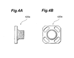
- the adapter 420 has a construction similar to that of FCN-AA-001 made by DDK Ltd., which comprises a sleeve 420a, two sleep holders 420b shaped equal to each other, two housings 420d and 420e shaped differently from each other, and two through four machine screws 420f.
- the adapter 420 and FCN-AA-001 according to the present invention are structured differently from each other at the side of the housing 420e.
- the screw holes which the machine screws 420f penetrate have a sectional shape that is not circular as in FCN-AA-001 but is like a broad bean. Namely, semicircles are disposed on both sides of two arcs around the center of the inner cylinder of the housing 420e, and the angle of the arc is set to 35 degrees. The radius of the semicircle is equal to that of the conventional circular screw hole. Accordingly, the seating surface is also sunk into a shape roughly similar to the screw hole. With this construction, while the plugs 400 and 410 are attached to both sides of the adapter 420, the plug 400 can be rotated relatively to the plug 410.
- the polarizer 90 formed of a circular polarizing filter is disposed in the hole of the holder 90a and fixed by a set screw 90b as appropriate.
- the filter is formed to be adjustable in angle by using a gear.
- the thickness measurement of a semiconductor wafer 200 by using this thickness measuring device 100 is described in detail.
- Light emitted from the measuring light source 6 is guided to the optical fiber 60, the optical connector 62, and the optical fiber 40.
- the light guided to the optical fiber 40 is partially made incident on the optical fiber 50 by the optical coupler 3, and guided to the reference optical system 9 via the optical connector 52, the optical fiber 51, and the optical plug 54.
- the light that has been made incident on the reference optical system 9 is reflected by the mirror 91 after passing through the glass substrate 92 and the polarizer 90, and then passes through the polarizer 90 and the glass substrate 92 and is made incident on the optical fiber 51 again via the optical plug 54, and thereafter, the light is guided to the optical fiber 50 via the optical connector 52.
- the light guided straight through the optical fiber 40 is guided to the probe head 7 via the optical connector 42, the optical fiber 41, and the optical plug 46, and irradiated onto the wafer 200.
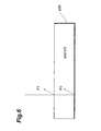
- the incident light is reflected by two points of the front and back surfaces.
- the light that has been made incident vertically is shown as if it is reflected diagonally, however, in actuality, the light made incident vertically is reflected perpendicularly.
- the reflected light is guided in reverse through the optical path of incidence, made incident on the probe head 7, guided to the optical fiber 40 via the optical plug 46, the optical fiber 41, and the optical connector 42, and then reaches the optical coupler 3 portion.
- the light that was reflected by the wafer 200 and returned to the optical fiber 40 and the light that reciprocated across the reference optical system 9 and returned to the optical fiber 50 are multiplexed and interfere with each other to generate interference light.
- the interference light thus generated is guided through the optical fiber 50 and transmitted to the photodetector 8 via the optical plug 53.
- the photodetector 8 converts the inputted intensity signal of the interference light into an electrical signal, etc., and transmits the signal to the signal processing part 20.
- the calculation part 22 calculates the thickness of the wafer 200 on the basis of a temporal intensity change obtained in the signal processing part 20 and the results of control of the optical path length control part 21.
- the interference light generated when the reference light and the reflected light coincide with each other in timing of reach becomes maximum in intensity when the polarization axes of the reference light and the reflected light coincide with each other.
- the polarization-preserving optical fibers are used for the most part of the waveguide, inside the same optical fiber (including the inside of the optical coupler 4), the plane of polarization is preserved.
- the straight polarized light in the direction of the main axis of polarization in the optical fiber of the upstream side is split into two components of straight polarized light in the direction of the main axis of polarization and straight polarized light orthogonal to this in the optical fiber at the downstream side.
- the refractive index is different between the direction of the main axis of polarization and the orthogonal direction, so that the propagation speed differs between these, and as light is guided through the optical fiber at the downstream side, the polarized light beam deviates.
- the reference light and the reflected light are generated in timing different from in the case where the main axes of polarization match each other, and accordingly, the generated interference light becomes noise.
- the intensity of the reflected light itself from the back surface of the wafer 200 is low while the intensity of the reflected light from the front surface is high, and as a result, noise generated according to the reflected light from the front surface increases, so that the noise may be more intensive than the reflected light from the back surface, and this makes measurement difficult.
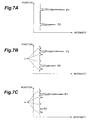
- Fig. 7A through Fig. 7C show the changes in output of the photodetector depending on the positional relationship of the main axes of polarization.
- the signal outputted from the photodetector 8 temporally changes as shown in Fig. 7A, and only two of the signal P1 corresponding to the reflection from the front surface and the signal P2 corresponding to the reflection from the back surface are obtained.
- noise n occurs.
- the impurity concentration of the semiconductor wafer 200 becomes higher, light absorption becomes greater, and as a result, the noise components produced by the signal P1 increase, so that it becomes difficult to distinguish the signal P2 and the noise components n as shown in Fig. 7C.
- this thickness measuring device 100 it is made possible to independently adjust the relative positions of the optical fibers to be connected by the optical connectors 42, 52, and 62 with respect to the optical axis. Thereby, by restraining the occurrence of noise by matching the main axes of polarization, measurement with high accuracy can be carried out. Furthermore, by making the angle of rotation of the polarizer 90 adjustable, noise occurring due to the rotation of the plane of polarization within the optical path in the space of the reference optical system 9 is restrained.
- the thickness measuring device 100 is operated by arranging a reference medium in place of the semiconductor wafer 20.
- a reference medium a medium that has a low transmittance and high reflectance on the front and back surfaces, for example, a glass substrate, etc., is preferable.
- Fig. 8 shows a signal intensity example. Noise that changes its intensity differs depending on the polarizer, so that adjustment is carried out by focusing on a signal component with a great intensity change (noise). However, it is influenced by other connectors and the change in angle of rotation of the polarizer, so that it is preferable that the adjustment is repeated until all noise components n become equal to or less than the permissible limit.
- the noise appears basically symmetrically for the original signal peaks S and P2, however, it is not strictly symmetrical, and even during adjustment, when one noise is reduced, the other one may become greater.
- noise that is highly necessary to be eliminated is the noise n that appears after the peak signals S and P2, that is, the noise n appearing below the peak signals S and P2 in Fig. 8, so that adjustment is carried out by focusing on this noise n.
- the optical fibers are fixed at the adjusted angles by tightening the machine screws. Performing this work while the signal intensity is monitored is preferable since it can be prevented that the angle deviates carelessly according to the tightening. Furthermore, by removing the plugs from the adapter of the side rotated after the adjustment and reattaching them, twisting of the optical fibers are eliminated and noise can be further reduced. This adjustment is not necessary for each measurement, and is carried out only in the case where the optical system is moved.
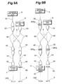
- Fig. 9B is a figure showing a modified example 1a of the Michelson interferometer 1 of the thickness measuring device 100 according to the present invention.
- the Michelson interferometer of Fig. 1 is shown in Fig. 9A.
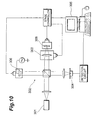
- polarizers 420g, 520g, 620g, and 70 disposed to be rotatable around the optical axis are provided between the plugs of the connectors 42, 52, and 62 and on the front end of the probe head 7.
- an adapter having a polarizer 420 disposed at the center is installed or a polarizer is disposed between two receptacles.
- polarization filters are disposed at all possible positions, however, the polarization filter is necessary at least at one of these positions.
- measurement of the thickness of a semiconductor wafer is taken as an example, however, the invention is also applicable to measurement of thickness of other optical transparent media.
- the thickness measuring device according to the present invention can be preferably used for thickness measurement of semiconductor wafers and other optical transparent media.
Landscapes
- Physics & Mathematics (AREA)
- General Physics & Mathematics (AREA)
- Length Measuring Devices By Optical Means (AREA)
Applications Claiming Priority (3)
| Application Number | Priority Date | Filing Date | Title |
|---|---|---|---|
| JP2002124599A JP2003315017A (ja) | 2002-04-25 | 2002-04-25 | 厚み計測装置 |
| JP2002124599 | 2002-04-25 | ||
| PCT/JP2003/005113 WO2003091659A1 (fr) | 2002-04-25 | 2003-04-22 | Dispositif de mesure d'epaisseur |
Publications (3)
| Publication Number | Publication Date |
|---|---|
| EP1498690A1 true EP1498690A1 (fr) | 2005-01-19 |
| EP1498690A4 EP1498690A4 (fr) | 2011-04-06 |
| EP1498690B1 EP1498690B1 (fr) | 2012-08-01 |
Family
ID=29267533
Family Applications (1)
| Application Number | Title | Priority Date | Filing Date |
|---|---|---|---|
| EP03719157A Expired - Lifetime EP1498690B1 (fr) | 2002-04-25 | 2003-04-22 | Dispositif de mesure d'epaisseur |
Country Status (5)
| Country | Link |
|---|---|
| US (1) | US20060152736A1 (fr) |
| EP (1) | EP1498690B1 (fr) |
| JP (1) | JP2003315017A (fr) |
| AU (1) | AU2003235351A1 (fr) |
| WO (1) | WO2003091659A1 (fr) |
Cited By (10)
| Publication number | Priority date | Publication date | Assignee | Title |
|---|---|---|---|---|
| FR2930334A1 (fr) * | 2008-04-22 | 2009-10-23 | Nanotec Solution Soc Civ Ile | Dispositif et procede d'analyse optique, appareil et procede de mesure chromatique associes |
| CN102538689A (zh) * | 2011-12-29 | 2012-07-04 | 中国科学院上海光学精密机械研究所 | 光学系统定心定位装置及其使用方法 |
| US20120281232A1 (en) * | 2011-05-06 | 2012-11-08 | Harris Corporation, Corporation Of The State Of Delaware | Interferometric material sensing apparatus including adjustable reference arm and associated methods |
| US20120281230A1 (en) * | 2011-05-06 | 2012-11-08 | Harris Corporation | Interferometric sensing apparatus including adjustable reference arm and associated methods |
| US20120281231A1 (en) * | 2011-05-06 | 2012-11-08 | Harris Corporation, Corporation Of The State Of Delaware | Interferometric biological sensing apparatus including adjustable reference arm and associated methods |
| US8649021B2 (en) | 2011-05-06 | 2014-02-11 | Harris Corporation | Interferometric sensing apparatus including adjustable coupling and associated methods |
| US8649022B2 (en) | 2011-05-06 | 2014-02-11 | Harris Corporation | Interferometric material sensing apparatus including adjustable coupling and associated methods |
| US8665451B2 (en) | 2011-05-06 | 2014-03-04 | Harris Corporation | Interferometric biometric sensing apparatus including adjustable coupling and associated methods |
| CN103940352A (zh) * | 2014-04-25 | 2014-07-23 | 广州飞拓优视光电科技有限公司 | 一种超高精度结冰探测装置及其实时探测结冰厚度方法 |
| CN108253891A (zh) * | 2016-12-28 | 2018-07-06 | 株式会社基恩士 | 光学扫描高度测量装置 |
Families Citing this family (1)
| Publication number | Priority date | Publication date | Assignee | Title |
|---|---|---|---|---|
| CN100395516C (zh) * | 2004-12-25 | 2008-06-18 | 鸿富锦精密工业(深圳)有限公司 | 光纤干涉式厚度测量装置 |
Family Cites Families (13)
| Publication number | Priority date | Publication date | Assignee | Title |
|---|---|---|---|---|
| US5255428A (en) * | 1991-04-03 | 1993-10-26 | California Institute Of Technology | Electrooptic polymer voltage sensor and method of manufacture thereof |
| US5206924A (en) | 1992-01-31 | 1993-04-27 | The United States Of America As Represented By The Secretary Of The Navy | Fiber optic Michelson sensor and arrays with passive elimination of polarization fading and source feedback isolation |
| US5422713A (en) * | 1994-03-21 | 1995-06-06 | The United States Of America As Represented By The Secretary Of The Navy | Bi-refringent waveguide rotational alignment method using white light interferomety |
| JPH0829641A (ja) * | 1994-07-11 | 1996-02-02 | Mitsubishi Electric Corp | 光ファイバ接続用アダプタ |
| US6172752B1 (en) * | 1996-08-04 | 2001-01-09 | Matsushita Electric Industrial Co., Ltd. | Method and apparatus for simultaneously interferometrically measuring optical characteristics in a noncontact manner |
| JP3582311B2 (ja) | 1996-08-04 | 2004-10-27 | 松下電器産業株式会社 | 媒質の測定方法および測定装置 |
| JPH10221014A (ja) | 1997-02-10 | 1998-08-21 | Sumitomo Metal Mining Co Ltd | 光導波路型変位センサ |
| JP4151159B2 (ja) * | 1999-06-17 | 2008-09-17 | 松下電器産業株式会社 | 媒質の測定装置 |
| US6201609B1 (en) * | 1999-08-27 | 2001-03-13 | Zygo Corporation | Interferometers utilizing polarization preserving optical systems |
| JP4464519B2 (ja) | 2000-03-21 | 2010-05-19 | オリンパス株式会社 | 光イメージング装置 |
| ATE396497T1 (de) * | 2000-01-21 | 2008-06-15 | Hamamatsu Photonics Kk | Dickenmessvorrichtung, dickenmessverfahren und nassätzvorrichtung und nassätzverfahren, die diese verwenden |
| JP4486217B2 (ja) * | 2000-05-01 | 2010-06-23 | 浜松ホトニクス株式会社 | 厚み計測装置、及びそれを用いたウエットエッチング装置、ウエットエッチング方法 |
| US20090030108A1 (en) | 2005-04-25 | 2009-01-29 | The University Of Tokyo | Gel composition and method for producing same |
-
2002
- 2002-04-25 JP JP2002124599A patent/JP2003315017A/ja active Pending
-
2003
- 2003-04-22 WO PCT/JP2003/005113 patent/WO2003091659A1/fr not_active Ceased
- 2003-04-22 EP EP03719157A patent/EP1498690B1/fr not_active Expired - Lifetime
- 2003-04-22 AU AU2003235351A patent/AU2003235351A1/en not_active Abandoned
- 2003-04-22 US US10/512,433 patent/US20060152736A1/en not_active Abandoned
Cited By (21)
| Publication number | Priority date | Publication date | Assignee | Title |
|---|---|---|---|---|
| FR2930334A1 (fr) * | 2008-04-22 | 2009-10-23 | Nanotec Solution Soc Civ Ile | Dispositif et procede d'analyse optique, appareil et procede de mesure chromatique associes |
| US8649021B2 (en) | 2011-05-06 | 2014-02-11 | Harris Corporation | Interferometric sensing apparatus including adjustable coupling and associated methods |
| US8665451B2 (en) | 2011-05-06 | 2014-03-04 | Harris Corporation | Interferometric biometric sensing apparatus including adjustable coupling and associated methods |
| US20120281230A1 (en) * | 2011-05-06 | 2012-11-08 | Harris Corporation | Interferometric sensing apparatus including adjustable reference arm and associated methods |
| US20120281231A1 (en) * | 2011-05-06 | 2012-11-08 | Harris Corporation, Corporation Of The State Of Delaware | Interferometric biological sensing apparatus including adjustable reference arm and associated methods |
| WO2012154386A1 (fr) * | 2011-05-06 | 2012-11-15 | Harris Corporation | Appareil de détection de matériau interférométrique comprenant un bras de référence réglable et procédés associés |
| WO2012154385A1 (fr) * | 2011-05-06 | 2012-11-15 | Harris Corporation | Appareil de détection biologique interférométrique comprenant un bras de référence réglable et procédés associés |
| US20120281232A1 (en) * | 2011-05-06 | 2012-11-08 | Harris Corporation, Corporation Of The State Of Delaware | Interferometric material sensing apparatus including adjustable reference arm and associated methods |
| US8649022B2 (en) | 2011-05-06 | 2014-02-11 | Harris Corporation | Interferometric material sensing apparatus including adjustable coupling and associated methods |
| WO2012154382A1 (fr) * | 2011-05-06 | 2012-11-15 | Harris Corporation | Appareil de détection interférométrique comprenant un bras de référence ajustable et procédés associés |
| US8976365B2 (en) | 2011-05-06 | 2015-03-10 | Harris Corporation | Interferometric material sensing apparatus including adjustable coupling and associated methods |
| US8842289B2 (en) | 2011-05-06 | 2014-09-23 | Harris Corporation | Interferometric biometric sensing apparatus including adjustable coupling and associated methods |
| US8675202B2 (en) * | 2011-05-06 | 2014-03-18 | Harris Corporation | Interferometric sensing apparatus including adjustable reference arm and associated methods |
| US8675204B2 (en) * | 2011-05-06 | 2014-03-18 | Harris Corporation | Interferometric material sensing apparatus including adjustable reference arm and associated methods |
| US8675203B2 (en) * | 2011-05-06 | 2014-03-18 | Harris Corporation | Interferometric biological sensing apparatus including adjustable reference arm and associated methods |
| US8842290B2 (en) | 2011-05-06 | 2014-09-23 | Harris Corporation | Interferometric sensing apparatus including adjustable coupling and associated methods |
| CN102538689B (zh) * | 2011-12-29 | 2014-02-12 | 中国科学院上海光学精密机械研究所 | 光学系统定心定位装置及其使用方法 |
| CN102538689A (zh) * | 2011-12-29 | 2012-07-04 | 中国科学院上海光学精密机械研究所 | 光学系统定心定位装置及其使用方法 |
| CN103940352A (zh) * | 2014-04-25 | 2014-07-23 | 广州飞拓优视光电科技有限公司 | 一种超高精度结冰探测装置及其实时探测结冰厚度方法 |
| CN108253891A (zh) * | 2016-12-28 | 2018-07-06 | 株式会社基恩士 | 光学扫描高度测量装置 |
| CN108253891B (zh) * | 2016-12-28 | 2021-10-26 | 株式会社基恩士 | 光学扫描高度测量装置 |
Also Published As
| Publication number | Publication date |
|---|---|
| EP1498690B1 (fr) | 2012-08-01 |
| EP1498690A4 (fr) | 2011-04-06 |
| US20060152736A1 (en) | 2006-07-13 |
| JP2003315017A (ja) | 2003-11-06 |
| WO2003091659A1 (fr) | 2003-11-06 |
| AU2003235351A1 (en) | 2003-11-10 |
Similar Documents
| Publication | Publication Date | Title |
|---|---|---|
| EP1103784B1 (fr) | Ellipsomètre | |
| US5563706A (en) | Interferometric surface profiler with an alignment optical member | |
| JP2997047B2 (ja) | 光学式計測装置 | |
| EP1498690B1 (fr) | Dispositif de mesure d'epaisseur | |
| JP2007260900A (ja) | ナノメートル接触検知方法および精密機械加工のための装置 | |
| WO2003075018A1 (fr) | Dispositif de mesure de courant | |
| WO2013038161A1 (fr) | Appareil permettant de mesurer la distribution des tailles de particules par diffusion de la lumière | |
| US5220397A (en) | Method and apparatus for angle measurement based on the internal reflection effect | |
| CN121230634A (zh) | 一种用于消除透明基底背散射的反射式干涉膜厚测量方法及系统 | |
| CN1656353A (zh) | 干涉测量式测量装置 | |
| CN218585050U (zh) | 固定夹具、光纤固定装置、激光耦合系统及激光系统 | |
| EP0823638B1 (fr) | Mesure de courant optique | |
| JPS63193003A (ja) | 凹部深さ・膜厚測定装置 | |
| US20070103694A1 (en) | Interferometry system | |
| CN221549838U (zh) | 基于多纵模正交激光自混合传感器的振动测量系统 | |
| RU2036418C1 (ru) | Устройство для определения толщины и оптических свойств слоев в процессе их формирования | |
| JP3405132B2 (ja) | コヒーレント光源の波面測定法 | |
| JPH068755B2 (ja) | 偏光度測定方法および装置 | |
| KR100422378B1 (ko) | 경사단면 광섬유 광원을 이용한 피조 간섭계 | |
| JP4713769B2 (ja) | 半導体レーザの高周波重畳動作検査装置 | |
| JP2985487B2 (ja) | 光波干渉計 | |
| JP2900052B2 (ja) | 微小変位計 | |
| EP0982580B1 (fr) | Ellipsometre | |
| JPH02116736A (ja) | 結晶方位決定方法およびその装置 | |
| JPH08285697A (ja) | 干渉計 |
Legal Events
| Date | Code | Title | Description |
|---|---|---|---|
| PUAI | Public reference made under article 153(3) epc to a published international application that has entered the european phase |
Free format text: ORIGINAL CODE: 0009012 |
|
| 17P | Request for examination filed |
Effective date: 20041101 |
|
| AK | Designated contracting states |
Kind code of ref document: A1 Designated state(s): AT BE BG CH CY CZ DE DK EE ES FI FR GB GR HU IE IT LI LU MC NL PT RO SE SI SK TR |
|
| AX | Request for extension of the european patent |
Extension state: AL LT LV MK |
|
| A4 | Supplementary search report drawn up and despatched |
Effective date: 20110308 |
|
| 17Q | First examination report despatched |
Effective date: 20110428 |
|
| GRAP | Despatch of communication of intention to grant a patent |
Free format text: ORIGINAL CODE: EPIDOSNIGR1 |
|
| RIC1 | Information provided on ipc code assigned before grant |
Ipc: G02B 6/02 20060101ALN20120125BHEP Ipc: G01B 9/02 20060101ALI20120125BHEP Ipc: G01B 11/06 20060101AFI20120125BHEP |
|
| GRAS | Grant fee paid |
Free format text: ORIGINAL CODE: EPIDOSNIGR3 |
|
| GRAA | (expected) grant |
Free format text: ORIGINAL CODE: 0009210 |
|
| AK | Designated contracting states |
Kind code of ref document: B1 Designated state(s): AT DE FR GB |
|
| REG | Reference to a national code |
Ref country code: GB Ref legal event code: FG4D |
|
| REG | Reference to a national code |
Ref country code: AT Ref legal event code: REF Ref document number: 568905 Country of ref document: AT Kind code of ref document: T Effective date: 20120815 |
|
| REG | Reference to a national code |
Ref country code: DE Ref legal event code: R096 Ref document number: 60341660 Country of ref document: DE Effective date: 20120927 |
|
| PLBE | No opposition filed within time limit |
Free format text: ORIGINAL CODE: 0009261 |
|
| STAA | Information on the status of an ep patent application or granted ep patent |
Free format text: STATUS: NO OPPOSITION FILED WITHIN TIME LIMIT |
|
| 26N | No opposition filed |
Effective date: 20130503 |
|
| REG | Reference to a national code |
Ref country code: DE Ref legal event code: R097 Ref document number: 60341660 Country of ref document: DE Effective date: 20130503 |
|
| GBPC | Gb: european patent ceased through non-payment of renewal fee |
Effective date: 20130422 |
|
| PG25 | Lapsed in a contracting state [announced via postgrant information from national office to epo] |
Ref country code: GB Free format text: LAPSE BECAUSE OF NON-PAYMENT OF DUE FEES Effective date: 20130422 Ref country code: DE Free format text: LAPSE BECAUSE OF NON-PAYMENT OF DUE FEES Effective date: 20131101 |
|
| REG | Reference to a national code |
Ref country code: FR Ref legal event code: ST Effective date: 20131231 |
|
| REG | Reference to a national code |
Ref country code: DE Ref legal event code: R119 Ref document number: 60341660 Country of ref document: DE Effective date: 20131101 |
|
| PG25 | Lapsed in a contracting state [announced via postgrant information from national office to epo] |
Ref country code: FR Free format text: LAPSE BECAUSE OF NON-PAYMENT OF DUE FEES Effective date: 20130430 |
|
| REG | Reference to a national code |
Ref country code: AT Ref legal event code: MM01 Ref document number: 568905 Country of ref document: AT Kind code of ref document: T Effective date: 20130422 |
|
| PG25 | Lapsed in a contracting state [announced via postgrant information from national office to epo] |
Ref country code: AT Free format text: LAPSE BECAUSE OF NON-PAYMENT OF DUE FEES Effective date: 20130422 |