EP1498870A2 - Verbindungselement und Ansteuerungseinrichtung für Plasmaanzeigetafel - Google Patents
Verbindungselement und Ansteuerungseinrichtung für Plasmaanzeigetafel Download PDFInfo
- Publication number
- EP1498870A2 EP1498870A2 EP04254244A EP04254244A EP1498870A2 EP 1498870 A2 EP1498870 A2 EP 1498870A2 EP 04254244 A EP04254244 A EP 04254244A EP 04254244 A EP04254244 A EP 04254244A EP 1498870 A2 EP1498870 A2 EP 1498870A2
- Authority
- EP
- European Patent Office
- Prior art keywords
- connection member
- driving device
- electrode pad
- scan
- common electrode
- Prior art date
- Legal status (The legal status is an assumption and is not a legal conclusion. Google has not performed a legal analysis and makes no representation as to the accuracy of the status listed.)
- Granted
Links
- 239000000758 substrate Substances 0.000 claims abstract description 55
- 239000011810 insulating material Substances 0.000 claims description 6
- 238000010586 diagram Methods 0.000 description 10
- 239000010410 layer Substances 0.000 description 8
- OAICVXFJPJFONN-UHFFFAOYSA-N Phosphorus Chemical compound [P] OAICVXFJPJFONN-UHFFFAOYSA-N 0.000 description 2
- 230000004888 barrier function Effects 0.000 description 2
- 238000004519 manufacturing process Methods 0.000 description 2
- 238000000034 method Methods 0.000 description 2
- 229910052698 phosphorus Inorganic materials 0.000 description 2
- 239000011574 phosphorus Substances 0.000 description 2
- 239000011241 protective layer Substances 0.000 description 2
- 238000011161 development Methods 0.000 description 1
- 230000018109 developmental process Effects 0.000 description 1
- 230000000694 effects Effects 0.000 description 1
- 239000004973 liquid crystal related substance Substances 0.000 description 1
- 230000006386 memory function Effects 0.000 description 1
- 238000012986 modification Methods 0.000 description 1
- 230000004048 modification Effects 0.000 description 1
- 230000008569 process Effects 0.000 description 1
Images


Classifications
-
- H—ELECTRICITY
- H05—ELECTRIC TECHNIQUES NOT OTHERWISE PROVIDED FOR
- H05K—PRINTED CIRCUITS; CASINGS OR CONSTRUCTIONAL DETAILS OF ELECTRIC APPARATUS; MANUFACTURE OF ASSEMBLAGES OF ELECTRICAL COMPONENTS
- H05K3/00—Apparatus or processes for manufacturing printed circuits
- H05K3/36—Assembling printed circuits with other printed circuits
- H05K3/361—Assembling flexible printed circuits with other printed circuits
-
- H—ELECTRICITY
- H04—ELECTRIC COMMUNICATION TECHNIQUE
- H04N—PICTORIAL COMMUNICATION, e.g. TELEVISION
- H04N5/00—Details of television systems
- H04N5/66—Transforming electric information into light information
-
- G—PHYSICS
- G09—EDUCATION; CRYPTOGRAPHY; DISPLAY; ADVERTISING; SEALS
- G09G—ARRANGEMENTS OR CIRCUITS FOR CONTROL OF INDICATING DEVICES USING STATIC MEANS TO PRESENT VARIABLE INFORMATION
- G09G3/00—Control arrangements or circuits, of interest only in connection with visual indicators other than cathode-ray tubes
- G09G3/20—Control arrangements or circuits, of interest only in connection with visual indicators other than cathode-ray tubes for presentation of an assembly of a number of characters, e.g. a page, by composing the assembly by combination of individual elements arranged in a matrix no fixed position being assigned to or needed to be assigned to the individual characters or partial characters
- G09G3/22—Control arrangements or circuits, of interest only in connection with visual indicators other than cathode-ray tubes for presentation of an assembly of a number of characters, e.g. a page, by composing the assembly by combination of individual elements arranged in a matrix no fixed position being assigned to or needed to be assigned to the individual characters or partial characters using controlled light sources
- G09G3/28—Control arrangements or circuits, of interest only in connection with visual indicators other than cathode-ray tubes for presentation of an assembly of a number of characters, e.g. a page, by composing the assembly by combination of individual elements arranged in a matrix no fixed position being assigned to or needed to be assigned to the individual characters or partial characters using controlled light sources using luminous gas-discharge panels, e.g. plasma panels
- G09G3/288—Control arrangements or circuits, of interest only in connection with visual indicators other than cathode-ray tubes for presentation of an assembly of a number of characters, e.g. a page, by composing the assembly by combination of individual elements arranged in a matrix no fixed position being assigned to or needed to be assigned to the individual characters or partial characters using controlled light sources using luminous gas-discharge panels, e.g. plasma panels using AC panels
- G09G3/296—Driving circuits for producing the waveforms applied to the driving electrodes
-
- H—ELECTRICITY
- H01—ELECTRIC ELEMENTS
- H01J—ELECTRIC DISCHARGE TUBES OR DISCHARGE LAMPS
- H01J11/00—Gas-filled discharge tubes with alternating current induction of the discharge, e.g. alternating current plasma display panels [AC-PDP]; Gas-filled discharge tubes without any main electrode inside the vessel; Gas-filled discharge tubes with at least one main electrode outside the vessel
- H01J11/10—AC-PDPs with at least one main electrode being out of contact with the plasma
- H01J11/12—AC-PDPs with at least one main electrode being out of contact with the plasma with main electrodes provided on both sides of the discharge space
-
- H—ELECTRICITY
- H01—ELECTRIC ELEMENTS
- H01J—ELECTRIC DISCHARGE TUBES OR DISCHARGE LAMPS
- H01J11/00—Gas-filled discharge tubes with alternating current induction of the discharge, e.g. alternating current plasma display panels [AC-PDP]; Gas-filled discharge tubes without any main electrode inside the vessel; Gas-filled discharge tubes with at least one main electrode outside the vessel
- H01J11/20—Constructional details
- H01J11/46—Connecting or feeding means, e.g. leading-in conductors
-
- G—PHYSICS
- G09—EDUCATION; CRYPTOGRAPHY; DISPLAY; ADVERTISING; SEALS
- G09G—ARRANGEMENTS OR CIRCUITS FOR CONTROL OF INDICATING DEVICES USING STATIC MEANS TO PRESENT VARIABLE INFORMATION
- G09G2300/00—Aspects of the constitution of display devices
- G09G2300/04—Structural and physical details of display devices
- G09G2300/0421—Structural details of the set of electrodes
- G09G2300/0426—Layout of electrodes and connections
-
- G—PHYSICS
- G09—EDUCATION; CRYPTOGRAPHY; DISPLAY; ADVERTISING; SEALS
- G09G—ARRANGEMENTS OR CIRCUITS FOR CONTROL OF INDICATING DEVICES USING STATIC MEANS TO PRESENT VARIABLE INFORMATION
- G09G2330/00—Aspects of power supply; Aspects of display protection and defect management
- G09G2330/08—Fault-tolerant or redundant circuits, or circuits in which repair of defects is prepared
-
- H—ELECTRICITY
- H01—ELECTRIC ELEMENTS
- H01J—ELECTRIC DISCHARGE TUBES OR DISCHARGE LAMPS
- H01J2211/00—Plasma display panels with alternate current induction of the discharge, e.g. AC-PDPs
- H01J2211/20—Constructional details
- H01J2211/46—Connecting or feeding means, e.g. leading-in conductors
-
- H—ELECTRICITY
- H05—ELECTRIC TECHNIQUES NOT OTHERWISE PROVIDED FOR
- H05K—PRINTED CIRCUITS; CASINGS OR CONSTRUCTIONAL DETAILS OF ELECTRIC APPARATUS; MANUFACTURE OF ASSEMBLAGES OF ELECTRICAL COMPONENTS
- H05K1/00—Printed circuits
- H05K1/02—Details
- H05K1/11—Printed elements for providing electric connections to or between printed circuits
- H05K1/117—Pads along the edge of rigid circuit boards, e.g. for pluggable connectors
-
- H—ELECTRICITY
- H05—ELECTRIC TECHNIQUES NOT OTHERWISE PROVIDED FOR
- H05K—PRINTED CIRCUITS; CASINGS OR CONSTRUCTIONAL DETAILS OF ELECTRIC APPARATUS; MANUFACTURE OF ASSEMBLAGES OF ELECTRICAL COMPONENTS
- H05K2201/00—Indexing scheme relating to printed circuits covered by H05K1/00
- H05K2201/09—Shape and layout
- H05K2201/09209—Shape and layout details of conductors
- H05K2201/09654—Shape and layout details of conductors covering at least two types of conductors provided for in H05K2201/09218 - H05K2201/095
- H05K2201/09709—Staggered pads, lands or terminals; Parallel conductors in different planes
Definitions
- the present invention relates to a plasma display panel, and more particularly to a connection member that connects an integrated board with an electrode and a driving device of a plasma display panel.
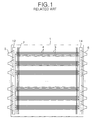
- FIG. 1 is a diagram representing a front substrate of a PDP in which electrodes are arranged according to the prior art.
- FIG. 2 is a diagram representing a rear substrate of a PDP with a driving device according to the prior art.
- an address electrode 2 is arranged and a scan electrode 3 and a common electrode 4 are arranged to cross the address electrode 2.
- a dielectric layer, a protective layer, barrier ribs and a phosphorus layer etc are formed in the front substrate by use of a plasma process technique though they are not shown in FIG. 1.
- a scan electrode terminal part 12 and a common electrode terminal part 14 leading to the scan electrode 3 and the common electrode 4 are provided at both sides in the front substrate 1.
- the rear substrate 7 includes connection members 5, 6 connecting each of electrode terminal parts 12, 14 with each of drivers 9, 10 in order to apply the driving signal generated at the scan driver 9 and the common driver 10 to the scan electrode 3 and the common electrode 4 of FIG. 1.
- the rear substrate 7 further includes a buffer 16 for applying the scan signal generated from the scan driver 9 to a corresponding scan electrode.
- the connection member 5 is connected between the buffer 16 and the scan electrode terminal part of the front substrate 1.
- the scan driver 9 generates the scan signal in accordance with the control signal and transmits it to the buffer 16.
- the buffer 16 finds the corresponding scan electrode on the basis of the scan signal and inputs the scan signal to the corresponding scan electrode through the connection member 5 and the scan electrode terminal part 12, thereby driving the corresponding scan electrode.
- the common driver 10 generates the common signal in accordance with the control signal of the controller 8 and applies the common signal to the common electrode 4 through the common electrode terminal part 14, thereby driving the common electrode 4.
- the driving device of prior art as above has the drivers 9 and 10, which drive the scan electrode 3 and the common electrode 4, separated from each other.
- the connection members 5 and 6 connected to the drivers 9 and 10 are also separated from each other.
- the area occupied by the components in the rear substrate is as broad as that, thereby resulting in the increase of the size.
- connection member except for designate parts of the end of the scan electrode pad and the common electrode pad, may be coated with an insulating material.
- the width of one joining part connected to the electrode terminal part may be at least wider than that of the other joining part connected to the integrated driving circuit.
- a driving device of or for a plasma display panel comprises: an integrated driving circuit installed at one side of a rear substrate to drive a scan electrode and a common electrode which are arranged on a front substrate; an electrode terminal part provided at a location opposite to the integrated driving circuit on the front substrate to lead to the scan electrode and the common electrode; and a connection member, wherein each of both joining parts has a two tier connection structure of a scan electrode pad and a common electrode pad, one joining part being connected to the integrated driving circuit, and the other joining part being connected to the electrode terminal part.
- Either of the scan electrode pad or the common electrode pad may be drawn out longer than the other.
- the driving device except for designate parts of the end of the scan electrode pad and the common electrode pad, may be coated with an insulating material.
- the width of one joining part connected to the electrode terminal part may be at least wider than that of the other joining part connected to the integrated driving circuit.
- connection member may have a first layer where scan electrode pads are arranged and a second layer where common electrode pads are arranged.
- the scan electrode pad and the common electrode pad may be arranged on the same surface in both of the joining parts of the connection member.
- the common signal may be input directly to the connection member without going through the applying means.
- FIG. 3 is a diagram representing a front substrate where all electrodes are arranged according to a desirable embodiment of the present invention.
- FIG. 4 is a diagram representing a rear substrate having a driving device according to a desirable embodiment of the present invention.
- address electrodes 52 are arranged in a front substrate 51 and scan electrodes 53 and the common electrodes 54 are arranged to cross the address electrodes 52 in the front substrate 51.
- a dielectric layer, a protective layer, barrier ribs and a phosphorus layer are formed in the front substrate 51 though they are not shown in FIG. 3.
- an electrode terminal part 66 leading to each of the scan electrode 53 and the common electrode 54 is provided at one side in the front substrate 51.
- the electrode terminal part is separated from the scan electrode terminal part 12 and the common electrode terminal part 14 and provided at each of both sides of the front substrate 1
- only one of the electrode terminal parts 66 is provided at one side of the front substrate 51 in the present invention.
- a driving device for applying a driving signal to each of electrodes 52, 53, 54 which are arranged in this way, is provided in the rear substrate 56 which is adhered to the front substrate 51 opposite thereto.
- the rear substrate 56 includes a controller 57 to control the driving signal, and an integrated driver 58 to generate a scan signal or a common signal in accordance with the control signal of the controller 57.
- the integrated driver 58 is connected to the controller 57 and provide at one side of the rear substrate 56.
- the integrated driver 58 is desirable to be provided in the rear substrate of the same side as the electrode terminal part 66 provide at one side of the front substrate 51 if possible.
- the driver is divided into the scan driver 9 and the common driver 10, but in the present invention, the driver is an integrated driver 58 of the prior art scan driver and common driver.
- the rear substrate 56 includes an address driver to generate a driving signal for driving an address electrode 52 of FIG. 3.
- connection member 55 is connected between the electrode terminal part 66 and the integrated driver 58 in order to apply a signal generated at the integrated driver 58 to the scan electrode 53 and the common electrode 54 of FIG. 3.
- FIG. 5 is a diagram representing a connection member according to a desirable embodiment according to the present invention.
- connection pads are arranged in the connection member 55.
- the connection member 55 is desirable to be a flexible printed circuit FPC.
- Scan electrode pads Y 61, 71 and common electrode pads Z 62, 72 are arranged in parallel. If the electrodes arranged in the front substrate 51, as shown in FIG. 3, are arranged in order of the scan electrode 53, the common electrode 54, the common electrode 54 and the scan electrode 53, the electrode pads arranged in the connection member 55 of the rear substrate 56 are desirable to be arranged in order of the scan electrode pads Y 61, 71, the common electrode pads Z 62, 72, the common electrode pads Z 62, 72, and the scan electrode pads Y 61, 71. Accordingly, the electrodes 53, 54 arranged on the front substrate 51 are correspondingly connected to the electrode pads 61, 62, 71, 72 arranged on the rear substrate.
- the ends of any one of the scan electrode pads 61, 71 or the common electrode pads 62, 72 is drawn out longer than the ends of the other.
- the distance between the ends of the scan electrode pads 61, 71 and common electrode pads 62, 72 become different in accordance with the distance or width between the electrode pads 61, 62, 71, 72, thus it might be set to be optimized upon designing.
- each of the scan electrode pads 61 71 and the common electrode pads 62, 72 are all coated with an insulating material except for designated parts 63, 64, 73, 74 of the ends 67, 68, 75, 76.
- the electrode pads 61, 62, 71, 72 corresponding to the designated parts 63, 64, 73, 74 are used when bonding the electrode terminal part 66 with the buffer 59.
- each electrode pad is made different in this way and the designated part except for the end of each electrode pad is coated with the insulating material, so that a short circuit, which might be generated between electrodes arranged with minute distance, can be prevented in advance, thereby preventing mis-operation from occurring upon driving.
- driver and connection member which were separated in the prior art, are integrated, thus having an effect of improving its drive characteristic when being controlled by the controller.
Landscapes
- Engineering & Computer Science (AREA)
- Physics & Mathematics (AREA)
- Plasma & Fusion (AREA)
- Computer Hardware Design (AREA)
- Power Engineering (AREA)
- General Physics & Mathematics (AREA)
- Theoretical Computer Science (AREA)
- Manufacturing & Machinery (AREA)
- Microelectronics & Electronic Packaging (AREA)
- Signal Processing (AREA)
- Multimedia (AREA)
- Devices For Indicating Variable Information By Combining Individual Elements (AREA)
- Control Of Indicators Other Than Cathode Ray Tubes (AREA)
- Gas-Filled Discharge Tubes (AREA)
Applications Claiming Priority (2)
| Application Number | Priority Date | Filing Date | Title |
|---|---|---|---|
| KR1020030048251A KR100571218B1 (ko) | 2003-07-15 | 2003-07-15 | 접속 부재 및 플라즈마 디스플레이 패널 구동 장치 |
| KR2003048251 | 2003-07-15 |
Publications (3)
| Publication Number | Publication Date |
|---|---|
| EP1498870A2 true EP1498870A2 (de) | 2005-01-19 |
| EP1498870A3 EP1498870A3 (de) | 2007-02-28 |
| EP1498870B1 EP1498870B1 (de) | 2011-03-09 |
Family
ID=33476022
Family Applications (1)
| Application Number | Title | Priority Date | Filing Date |
|---|---|---|---|
| EP04254244A Expired - Lifetime EP1498870B1 (de) | 2003-07-15 | 2004-07-15 | Plasmaanzeigetafel |
Country Status (6)
| Country | Link |
|---|---|
| US (1) | US7285917B2 (de) |
| EP (1) | EP1498870B1 (de) |
| JP (1) | JP2005037950A (de) |
| KR (1) | KR100571218B1 (de) |
| CN (1) | CN100477063C (de) |
| DE (1) | DE602004031695D1 (de) |
Cited By (1)
| Publication number | Priority date | Publication date | Assignee | Title |
|---|---|---|---|---|
| EP2051276A3 (de) * | 2005-04-06 | 2009-10-14 | Samsung SDI Co., Ltd. | Plasmaanzeigetafel |
Families Citing this family (8)
| Publication number | Priority date | Publication date | Assignee | Title |
|---|---|---|---|---|
| KR100573140B1 (ko) * | 2004-04-16 | 2006-04-24 | 삼성에스디아이 주식회사 | 플라즈마 디스플레이 패널 |
| US7375465B2 (en) * | 2005-05-19 | 2008-05-20 | Chunghwa Picture Tubes, Ltd. | Plasma display panel with single sided driving circuit |
| EP1724745A1 (de) * | 2005-05-20 | 2006-11-22 | LG Electronics Inc. | Plasmaanzeigevorrichtung und Verfahren zu ihrer Ansteuerung |
| KR100741131B1 (ko) * | 2006-06-20 | 2007-07-19 | 삼성에스디아이 주식회사 | 플라즈마 표시장치 |
| CN101401304B (zh) * | 2006-08-21 | 2011-04-13 | 株式会社村田制作所 | 高频模块 |
| KR20090031073A (ko) * | 2007-09-21 | 2009-03-25 | 엘지전자 주식회사 | 플라즈마 디스플레이 장치 |
| JP5063636B2 (ja) * | 2009-03-19 | 2012-10-31 | 篠田プラズマ株式会社 | 発光管アレイ型表示サブモジュール及び表示装置 |
| CN101969015A (zh) * | 2010-08-09 | 2011-02-09 | 安徽鑫昊等离子显示器件有限公司 | 一种等离子屏及其组合结构和其对应的fpc连接器 |
Citations (4)
| Publication number | Priority date | Publication date | Assignee | Title |
|---|---|---|---|---|
| JPH10255925A (ja) | 1997-03-11 | 1998-09-25 | Canon Inc | 接続装置 |
| JPH11344936A (ja) | 1998-06-02 | 1999-12-14 | Mitsubishi Electric Corp | プラズマディスプレイ表示装置 |
| US6563272B1 (en) | 2002-04-22 | 2003-05-13 | Koninklijke Philips Electronics N.V. | Combined scan/sustain driver for plasma display panel using dynamic gate drivers in SOI technology |
| JP2003178686A (ja) | 2001-12-13 | 2003-06-27 | Nec Kagoshima Ltd | プラズマディスプレイおよびその製造方法 |
Family Cites Families (29)
| Publication number | Priority date | Publication date | Assignee | Title |
|---|---|---|---|---|
| US3742296A (en) * | 1970-06-10 | 1973-06-26 | Ibm | Capacitive coupled connectors for gaseous discharge display panels |
| US4121135A (en) * | 1976-12-20 | 1978-10-17 | The Magnavox Company | Apparatus for interfacing with plasma type display panels |
| JPS5965825A (ja) * | 1982-10-08 | 1984-04-14 | Hitachi Ltd | 液晶表示素子 |
| JPS6021083A (ja) * | 1983-07-15 | 1985-02-02 | オプトレツクス株式会社 | 表示装置 |
| US4613855A (en) * | 1984-03-05 | 1986-09-23 | Dale Electronics, Inc. | Direct current dot matrix plasma display having integrated drivers |
| JPS6119285U (ja) * | 1984-07-06 | 1986-02-04 | 関西日本電気株式会社 | 薄膜elパネル |
| JPH0428145Y2 (de) * | 1987-09-09 | 1992-07-07 | ||
| JPH047522A (ja) * | 1990-04-25 | 1992-01-10 | Fujitsu Ltd | 液晶表示パネルの検査装置 |
| JPH05196953A (ja) * | 1992-01-22 | 1993-08-06 | Fujitsu Ltd | 配線フィルムの接続方法 |
| JP3298140B2 (ja) * | 1992-04-13 | 2002-07-02 | 富士通株式会社 | プラズマ・ディスプレイ・ユニットおよびプラズマ・ディスプレイ・パネル |
| JPH08179351A (ja) * | 1994-12-22 | 1996-07-12 | Toshiba Corp | 表示装置用アレイ基板 |
| JP2000082720A (ja) * | 1998-09-07 | 2000-03-21 | Canon Inc | 発光装置、露光装置及び画像形成装置 |
| FR2783928B1 (fr) * | 1998-09-28 | 2000-11-17 | St Microelectronics Sa | Procede de test de la connexion des sorties d'au moins un circuit de puissance pour ecran a plasma, et circuit de puissance pour sa mise en oeuvre |
| JP3298521B2 (ja) * | 1998-10-23 | 2002-07-02 | 日本電気株式会社 | プラズマ表示パネル |
| JP2000173481A (ja) | 1998-12-09 | 2000-06-23 | Hitachi Ltd | ガス放電型表示装置 |
| EP1065555A4 (de) * | 1999-01-20 | 2005-05-04 | Citizen Watch Co Ltd | Struktur zur befestigung einer halbleitervorrichtung auf einer flüssigkristallanzeige und eine halbleitervorrichtung |
| JP2000250425A (ja) * | 1999-02-25 | 2000-09-14 | Fujitsu Ltd | ドライバic実装モジュール |
| JP3450213B2 (ja) * | 1999-03-18 | 2003-09-22 | Necエレクトロニクス株式会社 | フラットパネル型表示装置 |
| JP2000347592A (ja) | 1999-06-09 | 2000-12-15 | Fujitsu Ltd | 平面表示パネルの電極端子接続方法 |
| JP4500403B2 (ja) * | 2000-03-17 | 2010-07-14 | キヤノン株式会社 | プラズマディスプレイパネルユニット |
| KR100701896B1 (ko) * | 2000-06-15 | 2007-03-30 | 엘지.필립스 엘시디 주식회사 | 액정표시소자와 그 제조방법 |
| KR100806808B1 (ko) * | 2000-10-17 | 2008-02-22 | 엘지.필립스 엘시디 주식회사 | 등저항 배선을 위한 액정표시장치 |
| JP2002244568A (ja) * | 2001-02-14 | 2002-08-30 | Matsushita Electric Ind Co Ltd | データ電極駆動装置 |
| KR100404200B1 (ko) * | 2001-07-12 | 2003-11-03 | 엘지전자 주식회사 | 유기 el 디스플레이 패널 |
| JP2003045338A (ja) * | 2001-07-30 | 2003-02-14 | Nec Corp | プラズマディスプレイ装置 |
| KR100592236B1 (ko) * | 2001-08-06 | 2006-06-21 | 삼성에스디아이 주식회사 | 통합 구동부를 가진 플라즈마 디스플레이 패널의 구동장치 |
| JP2003166901A (ja) * | 2001-11-30 | 2003-06-13 | Optrex Corp | 液晶パネル用点灯検査装置 |
| KR100828875B1 (ko) * | 2002-12-10 | 2008-05-09 | 오리온피디피주식회사 | 면방전 교류 플라즈마 디스플레이 패널의 플랙시블 기판 |
| KR100943900B1 (ko) * | 2003-05-23 | 2010-02-24 | 엘지전자 주식회사 | 플라즈마 디스플레이 패널 모듈 |
-
2003
- 2003-07-15 KR KR1020030048251A patent/KR100571218B1/ko not_active Expired - Fee Related
-
2004
- 2004-07-14 US US10/890,091 patent/US7285917B2/en not_active Expired - Fee Related
- 2004-07-15 JP JP2004208836A patent/JP2005037950A/ja active Pending
- 2004-07-15 CN CNB2004100900069A patent/CN100477063C/zh not_active Expired - Fee Related
- 2004-07-15 EP EP04254244A patent/EP1498870B1/de not_active Expired - Lifetime
- 2004-07-15 DE DE602004031695T patent/DE602004031695D1/de not_active Expired - Lifetime
Patent Citations (4)
| Publication number | Priority date | Publication date | Assignee | Title |
|---|---|---|---|---|
| JPH10255925A (ja) | 1997-03-11 | 1998-09-25 | Canon Inc | 接続装置 |
| JPH11344936A (ja) | 1998-06-02 | 1999-12-14 | Mitsubishi Electric Corp | プラズマディスプレイ表示装置 |
| JP2003178686A (ja) | 2001-12-13 | 2003-06-27 | Nec Kagoshima Ltd | プラズマディスプレイおよびその製造方法 |
| US6563272B1 (en) | 2002-04-22 | 2003-05-13 | Koninklijke Philips Electronics N.V. | Combined scan/sustain driver for plasma display panel using dynamic gate drivers in SOI technology |
Cited By (1)
| Publication number | Priority date | Publication date | Assignee | Title |
|---|---|---|---|---|
| EP2051276A3 (de) * | 2005-04-06 | 2009-10-14 | Samsung SDI Co., Ltd. | Plasmaanzeigetafel |
Also Published As
| Publication number | Publication date |
|---|---|
| JP2005037950A (ja) | 2005-02-10 |
| KR100571218B1 (ko) | 2006-04-13 |
| CN100477063C (zh) | 2009-04-08 |
| KR20050009010A (ko) | 2005-01-24 |
| EP1498870A3 (de) | 2007-02-28 |
| US7285917B2 (en) | 2007-10-23 |
| CN1599006A (zh) | 2005-03-23 |
| DE602004031695D1 (de) | 2011-04-21 |
| US20050012729A1 (en) | 2005-01-20 |
| EP1498870B1 (de) | 2011-03-09 |
Similar Documents
| Publication | Publication Date | Title |
|---|---|---|
| EP3261142B1 (de) | Anzeigevorrichtung mit einem biegebereich | |
| US8456384B2 (en) | Plasma display device | |
| US8836650B2 (en) | Touch-sensing display device | |
| EP3301665B1 (de) | Organische lichtemittierende anzeigevorrichtung | |
| US11378851B2 (en) | Display panel and display device | |
| JP2004213610A (ja) | タッチパネル | |
| EP1455377A2 (de) | Anzeigevorrichtung für Flachplattentyp | |
| EP1498870A2 (de) | Verbindungselement und Ansteuerungseinrichtung für Plasmaanzeigetafel | |
| JP2010092040A (ja) | プラズマディスプレイ装置 | |
| WO2021159845A1 (zh) | 显示面板和显示装置 | |
| JP2003005670A (ja) | 平面表示装置 | |
| JPH05290742A (ja) | プラズマ・ディスプレイ・ユニット | |
| JP2001215528A (ja) | 周辺駆動回路内蔵型液晶表示パネル | |
| JP2005107445A (ja) | 透明ディスプレイ構造体及び透明ディスプレイ表示装置 | |
| CN101533587B (zh) | 等离子体显示装置 | |
| JP2002324951A (ja) | フレキシブル接続基板およびこれを用いた回路ユニット | |
| US20110074759A1 (en) | Plasma display device | |
| KR20110124488A (ko) | 연성 기판과 이를 이용한 디스플레이 장치, 플라즈마 디스플레이 장치, 멀티 디스플레이 장치 및 멀티 플라즈마 디스플레이 장치 | |
| US20250355297A1 (en) | Display device | |
| KR20050020227A (ko) | 디스플레이 패널 | |
| KR100761297B1 (ko) | 플라즈마 디스플레이 장치 | |
| KR101072972B1 (ko) | 플라즈마 디스플레이 장치 | |
| KR102423525B1 (ko) | 디스플레이 장치 | |
| KR100610619B1 (ko) | 유기 전계발광표시장치 | |
| KR100856979B1 (ko) | 멀티 스크린형 플라즈마 디스플레이 장치 |
Legal Events
| Date | Code | Title | Description |
|---|---|---|---|
| PUAI | Public reference made under article 153(3) epc to a published international application that has entered the european phase |
Free format text: ORIGINAL CODE: 0009012 |
|
| AK | Designated contracting states |
Kind code of ref document: A2 Designated state(s): AT BE BG CH CY CZ DE DK EE ES FI FR GB GR HU IE IT LI LU MC NL PL PT RO SE SI SK TR |
|
| AX | Request for extension of the european patent |
Extension state: AL HR LT LV MK |
|
| PUAL | Search report despatched |
Free format text: ORIGINAL CODE: 0009013 |
|
| RIC1 | Information provided on ipc code assigned before grant |
Ipc: H01J 17/49 20060101AFI20070116BHEP Ipc: G09G 3/28 20060101ALI20070116BHEP Ipc: H05K 1/11 20060101ALI20070116BHEP |
|
| AK | Designated contracting states |
Kind code of ref document: A3 Designated state(s): AT BE BG CH CY CZ DE DK EE ES FI FR GB GR HU IE IT LI LU MC NL PL PT RO SE SI SK TR |
|
| AX | Request for extension of the european patent |
Extension state: AL HR LT LV MK |
|
| 17P | Request for examination filed |
Effective date: 20070419 |
|
| RIN1 | Information on inventor provided before grant (corrected) |
Inventor name: KIM, JIN YOUNG Inventor name: SHIN, SUNG GON |
|
| 17Q | First examination report despatched |
Effective date: 20071001 |
|
| AKX | Designation fees paid |
Designated state(s): DE FR GB NL |
|
| GRAP | Despatch of communication of intention to grant a patent |
Free format text: ORIGINAL CODE: EPIDOSNIGR1 |
|
| RTI1 | Title (correction) |
Free format text: PLASMA DISPLAY PANEL |
|
| GRAS | Grant fee paid |
Free format text: ORIGINAL CODE: EPIDOSNIGR3 |
|
| GRAA | (expected) grant |
Free format text: ORIGINAL CODE: 0009210 |
|
| AK | Designated contracting states |
Kind code of ref document: B1 Designated state(s): DE FR GB NL |
|
| REG | Reference to a national code |
Ref country code: GB Ref legal event code: FG4D |
|
| REF | Corresponds to: |
Ref document number: 602004031695 Country of ref document: DE Date of ref document: 20110421 Kind code of ref document: P |
|
| REG | Reference to a national code |
Ref country code: DE Ref legal event code: R096 Ref document number: 602004031695 Country of ref document: DE Effective date: 20110421 |
|
| REG | Reference to a national code |
Ref country code: NL Ref legal event code: VDEP Effective date: 20110309 |
|
| PG25 | Lapsed in a contracting state [announced via postgrant information from national office to epo] |
Ref country code: NL Free format text: LAPSE BECAUSE OF FAILURE TO SUBMIT A TRANSLATION OF THE DESCRIPTION OR TO PAY THE FEE WITHIN THE PRESCRIBED TIME-LIMIT Effective date: 20110309 |
|
| PLBE | No opposition filed within time limit |
Free format text: ORIGINAL CODE: 0009261 |
|
| STAA | Information on the status of an ep patent application or granted ep patent |
Free format text: STATUS: NO OPPOSITION FILED WITHIN TIME LIMIT |
|
| 26N | No opposition filed |
Effective date: 20111212 |
|
| GBPC | Gb: european patent ceased through non-payment of renewal fee |
Effective date: 20110715 |
|
| REG | Reference to a national code |
Ref country code: DE Ref legal event code: R097 Ref document number: 602004031695 Country of ref document: DE Effective date: 20111212 |
|
| REG | Reference to a national code |
Ref country code: FR Ref legal event code: ST Effective date: 20120330 |
|
| PG25 | Lapsed in a contracting state [announced via postgrant information from national office to epo] |
Ref country code: FR Free format text: LAPSE BECAUSE OF NON-PAYMENT OF DUE FEES Effective date: 20110801 |
|
| PG25 | Lapsed in a contracting state [announced via postgrant information from national office to epo] |
Ref country code: GB Free format text: LAPSE BECAUSE OF NON-PAYMENT OF DUE FEES Effective date: 20110715 |
|
| PGFP | Annual fee paid to national office [announced via postgrant information from national office to epo] |
Ref country code: DE Payment date: 20130611 Year of fee payment: 10 |
|
| REG | Reference to a national code |
Ref country code: DE Ref legal event code: R119 Ref document number: 602004031695 Country of ref document: DE |
|
| PG25 | Lapsed in a contracting state [announced via postgrant information from national office to epo] |
Ref country code: DE Free format text: LAPSE BECAUSE OF NON-PAYMENT OF DUE FEES Effective date: 20150203 |
|
| REG | Reference to a national code |
Ref country code: DE Ref legal event code: R119 Ref document number: 602004031695 Country of ref document: DE Effective date: 20150203 |