EP1498940A2 - Verwendung von Hypofluoriten, Fluorperoxyden, und/oder Fluortrioxyden als Oxidationsmittel in Fluorkohlenstoff- Ätzplasmmen - Google Patents
Verwendung von Hypofluoriten, Fluorperoxyden, und/oder Fluortrioxyden als Oxidationsmittel in Fluorkohlenstoff- Ätzplasmmen Download PDFInfo
- Publication number
- EP1498940A2 EP1498940A2 EP04016212A EP04016212A EP1498940A2 EP 1498940 A2 EP1498940 A2 EP 1498940A2 EP 04016212 A EP04016212 A EP 04016212A EP 04016212 A EP04016212 A EP 04016212A EP 1498940 A2 EP1498940 A2 EP 1498940A2
- Authority
- EP
- European Patent Office
- Prior art keywords
- mixture
- fluorocarbon
- combinations
- group
- dielectric material
- Prior art date
- Legal status (The legal status is an assumption and is not a legal conclusion. Google has not performed a legal analysis and makes no representation as to the accuracy of the status listed.)
- Withdrawn
Links
Images


Classifications
-
- C—CHEMISTRY; METALLURGY
- C09—DYES; PAINTS; POLISHES; NATURAL RESINS; ADHESIVES; COMPOSITIONS NOT OTHERWISE PROVIDED FOR; APPLICATIONS OF MATERIALS NOT OTHERWISE PROVIDED FOR
- C09K—MATERIALS FOR MISCELLANEOUS APPLICATIONS, NOT PROVIDED FOR ELSEWHERE
- C09K13/00—Etching, surface-brightening or pickling compositions
- C09K13/04—Etching, surface-brightening or pickling compositions containing an inorganic acid
- C09K13/08—Etching, surface-brightening or pickling compositions containing an inorganic acid containing a fluorine compound
-
- H—ELECTRICITY
- H10—SEMICONDUCTOR DEVICES; ELECTRIC SOLID-STATE DEVICES NOT OTHERWISE PROVIDED FOR
- H10P—GENERIC PROCESSES OR APPARATUS FOR THE MANUFACTURE OR TREATMENT OF DEVICES COVERED BY CLASS H10
- H10P50/00—Etching of wafers, substrates or parts of devices
- H10P50/20—Dry etching; Plasma etching; Reactive-ion etching
- H10P50/28—Dry etching; Plasma etching; Reactive-ion etching of insulating materials
- H10P50/282—Dry etching; Plasma etching; Reactive-ion etching of insulating materials of inorganic materials
- H10P50/283—Dry etching; Plasma etching; Reactive-ion etching of insulating materials of inorganic materials by chemical means
-
- H—ELECTRICITY
- H10—SEMICONDUCTOR DEVICES; ELECTRIC SOLID-STATE DEVICES NOT OTHERWISE PROVIDED FOR
- H10P—GENERIC PROCESSES OR APPARATUS FOR THE MANUFACTURE OR TREATMENT OF DEVICES COVERED BY CLASS H10
- H10P50/00—Etching of wafers, substrates or parts of devices
- H10P50/60—Wet etching
- H10P50/64—Wet etching of semiconductor materials
- H10P50/642—Chemical etching
-
- C—CHEMISTRY; METALLURGY
- C11—ANIMAL OR VEGETABLE OILS, FATS, FATTY SUBSTANCES OR WAXES; FATTY ACIDS THEREFROM; DETERGENTS; CANDLES
- C11D—DETERGENT COMPOSITIONS; USE OF SINGLE SUBSTANCES AS DETERGENTS; SOAP OR SOAP-MAKING; RESIN SOAPS; RECOVERY OF GLYCEROL
- C11D2111/00—Cleaning compositions characterised by the objects to be cleaned; Cleaning compositions characterised by non-standard cleaning or washing processes
- C11D2111/10—Objects to be cleaned
- C11D2111/14—Hard surfaces
- C11D2111/22—Electronic devices, e.g. PCBs or semiconductors
Definitions
- Dielectric materials are principally used for forming electrically insulating layers within, for example, an electronic device or integrated circuits (IC). Selective anisotropic etching of dielectric materials is the process step extensively used to produce features in the manufacturing of integrated circuits (IC), microelectromechanical systems (MEMS), optoelectronic devices, and micro-optoelectronic-mechanical systems (MOEMS).
- IC integrated circuits
- MEMS microelectromechanical systems
- MOEMS micro-optoelectronic-mechanical systems
- patterned masks are generally composed of an organic photoresist material; however "hard” mask materials, such as silicon nitride Si 3 N 4 , or other material that may be etched at a slower rate than the dielectric material, may also be used as the mask material. Selective anisotropic etching allows for the formation of features such as contact and via holes by removing at least a portion of the underlying dielectric material while essentially preserving the patterned mask.
- the dielectric materials to be selectively removed from under the mask openings include: silicon in its various forms such as crystalline silicon, polysilicon, amorphous silicon, and epitaxial silicon; compositions containing silicon such as silicon dioxide (SiO 2 ); undoped silicate glass (USG); doped silicate glass such as boron doped silicate glass (BSG); phosphorous doped silicate glass (PSG), and borophosphosilicate glass (BPSG); silicon and nitrogen containing materials such as silicon nitride (Si 3 N 4 ), silicon carbonitride (SiCN) and silicon oxynitride (SiON); and materials having a low dielectric constant (e.g., having a dielectric constant of 4.2 or less) such as fluorine doped silicate glass (FSG), organosilicate glass (OSG), organofluoro-silicate glass (OFSG), polymeric materials such as silsesquioxanes (HSQ, HSiO 1.5 ) and methyl silses
- Some of the key manufacturing requirements for selective anisotropic dielectric etching include: high etch rate of the underlying dielectric materials; zero or low loss of the patterned mask, i.e., high etch selectivity of the dielectric material over the mask material; maintaining the critical dimensions of the patterned mask; maintaining desired etch profile, i.e. high anisotropy; maintaining uniformity across the wafer; minimal variation over feature sizes and density, i.e., no microloading effects; high selectivity over underlying etch stop layer such as SiC, SiN, and silicon etc.; and sidewall passivation films that can be easily removed in post-etch ashing, stripping and/or rinsing.
- achieving high etch selectivity of the dielectric materials over the mask material and maintaining the critical dimensions of the patterned mask may be the most important yet the most challenging performance requirements to obtain.
- DUV photoresist materials are increasingly being adopted for deep ultraviolet (DUV) photolithography at sub-200 nm, i.e., 193 nm, wavelengths.
- DUV photoresist materials are generally less resistant to plasma etching than older-generation photoresist materials.
- the thickness of the DUV photoresist is typically only a few hundreds of nanometers, and in some instances less than 200 nm, because of the absorptivity of DUV light by the resist materials. Because of the limits set by dielectric break-down, the thickness of the dielectric layer are generally not reduced below 0.5 to 1 ⁇ m. However, the minimum feature sizes of the contact and via holes penetrating the dielectric layer may be below 0.5 ⁇ m.
- the holes etched within the dielectric material need to be highly anisotropic and have high aspect ratios (HAR), defined as the ratio of the depth to the minimum width of a hole.
- High aspect ratio (HAR) etching of dielectric materials may require via/trench depth of over several micrometers or an order of magnitude higher than the thickness of the DUV.
- the further evolution of photolithography technology to lower wavelengths, i.e., 157 nm and EUV photolithography, may lead to the need for even higher etch selectivity between the underlying dielectric materials and the photoresist materials.
- Fluorocarbon plasmas are commonly used for selective anisotropic etching of silicon-containing dielectric materials such as SiO 2 .
- the fluorocarbons used for selective anisotropic etching include: CF 4 (tetrafluoromethane), CHF 3 (trifluoromethane), C 4 F 8 (octafluorocyclobutane), C 5 F 8 (octafluorocyclopentene), and C 4 F 6 (hexafluoro-1,3-butadiene). These fluorocarbons dissociate in plasma to form reactive fluorocarbon species, such as, for example CF, CF 2 , C 2 F 3 etc.
- the fluorocarbon species may provide the reactive source of fluorine to etch the underlying silicon-containing dielectric materials in the presence of, for example, energetic ion bombardment. Further, the fluorocarbon species may form a fluorocarbon polymer that protects the photoresist and the sidewalls of the etch features which is referred to herein as the polymerization reaction.
- the substrate typically contains one or more dielectric layers covered with a patterned photoresist coating to provide a feature such as a contact or via hole within the dielectric material.
- the fluorocarbon polymer may initiate distinctly different plasma-surface chemical reactions.
- the fluorocarbon polymer may form a protective layer against sputtering damage of argon ions and/or other reactive species in the plasma at the photoresist surface.
- the presence of oxygen within the dielectric material and high energy ions impinging upon the exposed dielectric surface may facilitate the formation of volatile species which is referred to herein as the etch reaction.
- the volatile species formed from the etch reaction can be readily removed from the reactor via vacuum pump or other means.
- the etch reaction does not typically occur on the sidewall surfaces of vias or trenches since there is no ion bombardment impinging upon the vertical surfaces. Therefore, the fluorocarbon polymer may provide a protective or passivation layer on the unexposed dielectric material such as feature sidewalls whereas the etch reaction of the fluorocarbon polymer with the exposed dielectric forms volatile species thereby removing the dielectric material.
- the end-product of the polymerization reaction, or the fluorocarbon polymer serves as source for the reactive fluorine in the etch reaction, provided that it can be adequately removed so that no fluorocarbon polymer accumulates on the exposed dielectric surface thereby impeding the etching process.
- etching reaction cannot compete with the polymerization reaction, the thin fluorocarbon film can accumulate and the etch process may stop.
- molecular oxygen (O 2 ) is routinely added to the fluorocarbon etch plasma.
- the etch rate of the dielectric material may be increased if an optimal balance between the competing reactions can be achieved.
- O 2 can attack the organic photoresist materials thereby increasing the photoresist etch rate. This may result in the undesirable decrease of etch selectivity of the dielectric material over the photoresist material within the substrate.
- European Patent Application EP 0924282 describes the use of hypofluorites by themselves or in a mixture with an inert gas, a hydrogen or hydrogen-containing gas (e.g., HI, HBr, HCl, CH 4 , NH 3 , H 2 , C 2 H 2 , and C 2 H 6 ), and/or an oxygen or oxygen-containing gas (i.e., CO, NO, N 2 O, and NO 2 ) as a replacement for fluorocarbon gases.
- a hydrogen or hydrogen-containing gas e.g., HI, HBr, HCl, CH 4 , NH 3 , H 2 , C 2 H 2 , and C 2 H 6
- an oxygen or oxygen-containing gas i.e., CO, NO, N 2 O, and NO 2
- Japanese Patent Application JP 2000/038581A describes the use of bis-trifluoromethyl peroxide as an etch gas by itself or in a mixture containing a hydrogen or hydrogen-containing gas.
- Japanese Patent Applications JP 2000/038675A and JP 2002/184765A describe the use of bis-trifluoromethyl peroxide, fluoroxytrifluoromethane (FTM), or bis-(fluoroxy)difluoromethane (BDM) as a cleaning gas to remove deposits from CVD chambers.
- FTM fluoroxytrifluoromethane
- BDM bis-(fluoroxy)difluoromethane
- the present invention satisfies one, if not all, of the needs in the art by providing a mixture and a method comprising same for removing at least a portion of a dielectric material from a layered substrate.
- a mixture for etching a dielectric material in a layered substrate comprising: a fluorocarbon and an oxidizer selected from the group consisting of a hypofluorite, a fluoroperoxide, a fluorotrioxide, and combinations thereof.
- a mixture for etching a dielectric material in a layered substrate comprising: a fluorocarbon and a hypofluorite.
- a mixture for etching a dielectric material in a layered substrate comprising: a fluorocarbon and a fluoroperoxide.
- a mixture for etching a dielectric material in a layered substrate comprising: a fluorocarbon and a fluorotrioxide.
- a method for the removal of a portion of a dielectric material from a layered substrate comprising: placing the layered substrate within a reaction chamber; providing a gas mixture comprising a fluorocarbon gas and an oxidizer gas selected from the group consisting of a hypofluorite, a fluoroperoxide, a fluorotrioxide, and combinations thereof; applying energy to the gas mixture to form active species; and contacting the layered substrate with the active species wherein the active species react with and remove the portion of the dielectric material.
- a method for etching at least a portion of a dielectric material from a layered substrate comprising: contacting the layered substrate with the active species of a mixture comprising a fluorocarbon, an oxidizer selected from the group consisting of a hypofluorite, a fluoroperoxide, a fluorotrioxide, and combinations thereof, wherein the active species at least partially reacts with and removes at least a portion of the dielectric material.
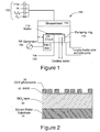
- Figure 1 provides an illustration of an apparatus used in one embodiment of the method of the present invention.
- Figure 2 provides an example of a layered substrate.
- Figure 3 provides a Scanning Electron Microscopy (SEM) image of a 0.35 ⁇ m via that was etched using one embodiment of the method of the present invention.
- Figure 4 provides a SEM image of a 0.5 ⁇ m via that was etched using one embodiment of the method of the present invention.
- Figure 5 provides a SEM image of a 0.35 ⁇ m via that was etched using a comparative method.
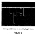
- Figure 6 provides a SEM image of a 0.5 ⁇ m via that was etched using a comparative method.
- Figure 7 provides a SEM image of a 0.3 ⁇ m that was etched using one embodiment of the method of the present invention.
- the present invention provides a mixture and a method comprising same for the removal of a substance from a layered substrate, that uses a fluorine-containing oxidizer such as hypofluorites, fluoro-peroxides, and/or fluoro-trioxides to decrease the amount of, or replace, molecular oxygen (O 2 ) as the oxidizer, in conjunction with one or more fluorocarbons.
- a fluorine-containing oxidizer such as hypofluorites, fluoro-peroxides, and/or fluoro-trioxides to decrease the amount of, or replace, molecular oxygen (O 2 ) as the oxidizer, in conjunction with one or more fluorocarbons.
- the mixture and the method of the present invention may be used, for example, for selective anisotropic etching of a dielectric material from a layered substrate.
- the mixture may be exposed to one or more energy sources sufficient to form active species, which then react with and remove the substance from the substrate.
- a fluorine-containing oxidizer such as a hypofluorite, a fluoroperoxide, and/or a fluorotrioxide may be used in place of some, if not all of the O 2 , thereby preventing the erosion of the mask or photoresist material.
- the fluorine-containing oxidizer may increase the dielectric etch rate by providing additional fluorine atoms into the etch reaction and subsequently the dielectric surface.
- hypofluorites, fluoro-peroxides, and/or fluorotrioxides may enhance both the etch rate of dielectric materials and the etch selectivity of dielectric materials over photoresist materials.
- the mixture of the present invention comprises the following reagents: at least one fluorocarbon and a fluorine-containing oxidizer such as a hypofluorite, a fluoroperoxide, and/or a fluorotrioxide.
- a fluorine-containing oxidizer such as a hypofluorite, a fluoroperoxide, and/or a fluorotrioxide.
- the mixture of the present invention contains one or more fluorocarbon gases in conjunction with the one or more fluorine-containing oxidizer.
- fluorocarbon as used herein includes perfluorocarbons (compounds containing C and F atoms), hydrofluorocarbons (compounds containing C, H, and F), oxyhydrofluorocarbons (compounds containing C, H, O, and F), and oxyfluorocarbons (compounds containing C, O, and F).
- the perfluorocarbon is a compound having the formula C h F i wherein h is a number ranging from 1 to 10 and i is a number ranging from h to 2h+2.
- perfluorocarbons having the formula C h F i include, but are not limited to, CF 4 (tetrafluoromethane), C 4 F 8 (octafluorocyclobutane), C 5 F 8 (octafluorocyclopentene), and C 4 F 6 (hexafluoro-1,3-butadiene).
- the fluorocarbon is a hydrofluorocarbon compound having the formula C j H k F l wherein j is a number from 1 to 10, and k and l are positive integers with (k + l) from j to 2j + 2.
- hydrofluorocarbon compound having the formula C j H k F l includes CHF 3 (trifluoromethane).
- the fluorocarbon is an oxyfluorocarbon or a oxyhydrofluorocarbon.
- oxyfluorocarbon compounds include perfluorocyclopentene oxide, hexafluoro-cyclobutanone, hexafluorodihydrofuran, hexafluorobutadiene epoxide, tetrafluorocyclobutanedione perfluorotetrahydrofuran (C 4 F 8 O), hexafluoropropylene oxide (C 3 F 6 O), perfluoromethylvinyl ether (C 3 F 6 O), and combinations thereof.
- An example of a oxyhydrofluorocarbon compound includes heptafluorocyclobutanol.
- the amount of fluorocarbon gas present in the mixture may range from 1 to 99%, preferably from 1 to 50%, and more preferably from 2 to 20% by volume.
- F/C ratio a fluorocarbon with a lower ratio of fluorine atoms to carbon atoms
- F/C ratio a fluorocarbon with a lower ratio of fluorine atoms to carbon atoms
- F/C ratio a fluorocarbon with a lower ratio of fluorine atoms to carbon atoms
- the etch plasmas can form fluorocarbon polymers having a higher degree of cross-linking. Highly cross-linked fluorocarbon polymers may be more resistant to the etch reaction thereby providing better protection to the photoresist layer and sidewalls.
- other fluorocarbons having a F/C of 2 or greater may also be used.
- the mixture of the present invention contains at least one fluorine-containing oxidizer gas selected from the group consisting of a hypofluorite, a fluoroperoxide, a fluorotrioxide, or a combination thereof.
- a hypofluorite refers to a molecule that contains at least one -O-F group.
- the hypofluorite preferably is a compound having the formula C x H y F z (OF) n O m wherein x is a number ranging from 0 to 8, y is a number ranging from 0 to 17, z is a number ranging from 0 to 17, n is 1 or 2, and m is 0, 1, or 2.
- hypofluorites include fluoroxytrifluoromethane (FTM, CF 3 -O-F), methylhypofluorite (CH 3 OF), hypofluorous acid (HOF), trifluoroacetyl hypofluorite (CF 3 C(O)OF), acetyl hypofluorite (CH 3 C(O)OF), and bis-(fluoroxy)difluoromethane (BDM, F-O-CF 2 -O-F).
- FTM fluoroxytrifluoromethane
- CH 3 OF methylhypofluorite
- HAF hypofluorous acid
- BDM bis-(fluoroxy)difluoromethane
- a fluoroperoxide, as described herein, is a molecule that contains at least one -O-O- group and where some if not all of the hydrogen atoms in the molecule are replaced with fluorine atoms.
- fluoro-peroxides examples include F-O-O-F (difluoro-peroxide), CF 3 -O-O-F (fluoro-trifluoromethyl-peroxide), CF 3 -O-O-CF 3 (bis-trifluoromethyl peroxide), CF 3 -O-O-C 2 F 5 (pentafluoroethyl-trifluoromethyl-peroxide), C 2 F 5 -O-O-C 2 F 5 (bis-pentafluoroethyl-peroxide), CF 2 O 2 (difluorodioxirane), CF 3 OC(O)OOC(O)OCF 3 (bis-trifluoromethyl peroxydicarbonate), and CF 3 -O-O-C(O)F (fluoroformyl trifluoromethyl peroxide), and FC(O)-O-O-C(O)F (bis-fluoroformyl trifluoromethyl peroxide),
- a fluoro-trioxide is a molecule that contains at least one -O-O-O- group and where some or all of the hydrogen atoms in the molecule are replaced with fluorine atoms.
- fluorotrioxides include CF 3 -O-O-O-CF 3 (bis-trifluoromethyl-trioxide), CF 3 -O-O-O-F (fluorotrifluoromethyl-trioxide), and CF 3 -O-O-O-C(O)F (fluoroformyl trifluoromethyl-trioxide).
- the amount of fluorine-containing oxidizer gas present in the mixture may range from 1 to 99%, preferably from 1 to 75%, and more preferably from 1 to 50% by volume.
- the ratio by volume of the fluorine-containing oxidizer gas to fluorocarbon gas within the mixture may range from 0.1:1 to 20:1, preferably from 0.1:1 to 10:1, and more preferably from 0.1:1 to 5:1.
- inert diluent gases such as argon, nitrogen, helium, neon, krypton, xenon or combinations thereof can also be added.
- Inert diluent gases can, for example, modify the plasma characteristics to better suit some specific applications.
- ions from inert gases such as, for example, argon may provide the energetic bombardment to facilitate the selective anisotropic etch reactions.
- concentration of the inert gas within the mixture can range from 0 to 99%, preferably from 25 to 99%, and more preferably from 50 to 99% by volume.
- the mixture may further comprise an oxidizer such as, for example, O 2 , O 3 , CO, CO 2 , and N 2 O.
- an oxidizer such as, for example, O 2 , O 3 , CO, CO 2 , and N 2 O.
- the amount of oxidizer present in the mixture may range from 0 to 99 %, preferably from 0 to 75 %, and more preferably from 0 to 50 % by volume.
- the chemical reagents can be delivered to the reaction chamber by a variety of means, such as, for example, conventional cylinders, safe delivery systems, vacuum delivery systems, solid or liquid-based generators that create the chemical reagent and/or the gas mixture at the point of use (POU).
- the hypofluorites, fluoroperoxides, and/or fluorotrioxides can be delivered to the reaction chamber via a compressed gas cylinder.
- the chemical reagent such as the hypofluorite FTM can be generated at the point of use through, for example, the reaction of 1 or 2 molar equivalents of fluorine gas (F 2 ) with COF 2 or CO, respectively, in the presence of a catalyst.
- the hypofluorite BDM can be generated at the point of use through the reaction of 2 molar equivalents of fluorine gas with CO 2 in the presence of a catalyst.
- the source of F 2 and COF 2 in the foregoing reactions can be from a compressed cylinder, a safe delivery system, or a vacuum delivery system. Additionally, F 2 can be generated at the point of use via electrolytic dissociation of 2 molar equivalents of HF to form H 2 and F 2 .
- the process of the invention is useful for etching substances such as a dielectric material from a substrate.
- Suitable substrates include, but are not limited to, semiconductor materials such as gallium arsenide (“GaAs”), boron nitride (“BN”), silicon in its various forms such as crystalline silicon, polysilicon, amorphous silicon, and epitaxial silicon, compositions containing silicon such as silicon dioxide (“SiO 2 "), silicon carbide (“SiC”), silicon oxycarbide (“SiOC”), silicon nitride (“SiN”), silicon carbonitride (“SiCN”), organosilicate glasses (“OSG”), organofluorosilicate glasses (“OFSG”), fluorosilicate glasses (“FSG”), and other appropriate substrates or mixtures thereof.
- semiconductor materials such as gallium arsenide (“GaAs”), boron nitride (“BN”)
- Si in its various forms such as crystalline silicon, polysilicon, amorphous silicon, and
- Substrates may further comprise a variety of layers that include, for example, anti reflective coatings, photoresists, organic polymers, porous organic and inorganic materials, metals such as copper and aluminum, or diffusion barrier layers, e.g., TiN, Ti(C)N, TaN, Ta(C)N, Ta, W, WN, or W(C)N.
- layers that include, for example, anti reflective coatings, photoresists, organic polymers, porous organic and inorganic materials, metals such as copper and aluminum, or diffusion barrier layers, e.g., TiN, Ti(C)N, TaN, Ta(C)N, Ta, W, WN, or W(C)N.
- Figure 2 provides an example of a layered silicon wafer substrate 10 that is suitable for etching using the method of the present invention.
- Substrate 10 has a dielectric layer 20 such as SiO 2 deposited thereupon.
- a mask layer 30 such as a DUV photoresist is applied to dielectric layer 20 atop a back-side anti-reflective coating (BARC).
- BARC back-side anti-reflective coating
- a patterned photoresist is typically formed by exposing the substrate to a radiation source to provide an image, and developing the substrate to form a patterned photoresist layer on the substrate.
- This patterned layer then acts as a mask for subsequent substrate patterning processes such as etching, doping, and/or coating with metals, other semiconductor materials, or insulating materials.
- the selective anisotropic etching process generally involves removing the portion of the substrate surface that is not protected by the patterned photoresist thereby exposing the underlying surface for further processing.
- the mixture of the present invention is exposed to one or more energy sources sufficient to generate active species to at least partially react with the dielectric material and form volatile species.
- the energy source for the exposing step may include, but not be limited to, ⁇ -particles, ⁇ -particles, ⁇ -rays, x-rays, high energy electron, electron beam sources of energy, ultraviolet (wavelengths ranging from 10 to 400 nm), visible (wavelengths ranging from 400 to 750 nm), infrared (wavelengths ranging from 750 to 10 5 nm), microwave (frequency > 10 9 Hz), radio-frequency wave (frequency > 10 6 Hz) energy; thermal, RF, DC, arc or corona discharge, sonic, ultrasonic or megasonic energy, and combinations thereof.
- the mixture is exposed to an energy source sufficient to generate a plasma having active species contained therein.
- etching processes include, but are not limited to, reactive ion etch (RIE), magnetically enhanced reactive ion etch (MERIE), a inductively coupled plasma (ICP) with or without a separate bias power source, transformer coupled plasma (TCP), hollow anode type plasma, helical resonator plasma, electron cyclotron resonance (ECR) with or without a separate bias power source, RF or microwave excited high density plasma source with or without a separate bias power source, etc.
- RIE reactive ion etch
- MIE magnetically enhanced reactive ion etch
- ICP inductively coupled plasma
- TCP transformer coupled plasma
- hollow anode type plasma helical resonator plasma
- ECR electron cyclotron resonance
- the etching process is conducted using a capacitively coupled parallel plate reaction chamber.
- the layered substrate (e.g., a patterned wafer) may be placed onto a RF powered lower electrode within a reaction chamber.
- the substrate is held onto the electrode by either a mechanical clamping ring or an electrostatic chuck.
- the backside of the substrate may be cooled with an inert gas such as helium.
- the RF power source may be, for example, an RF generator operating at a frequency of 13.56 MHz, however other frequencies can also be used.
- the RF power density can vary from 0.3 to 30 W/cm 2 , preferably from 1 to 16 W/cm 2 .
- the operating pressure can vary from 0.1 to 10,000 mTorr, preferably from 1 to 1000 mTorr, and more preferably from 1 to 100 mTorr.
- the flow rate of the mixture into the reaction chamber ranges from 10 to 50,000 standard cubic centimeters per minute (sccm), preferably from 20 to 10,000 sccm, and more preferably from 25 to 1,000 scc
- etch reactors a modified Gaseous Electronics Conference Reference Reactor ("GEC") plasma reactor and a commercial production scale Applied Materials P-5000 Mark II reactor.
- the experiments were conducted in a parallel plate capacitively coupled RF plasma reactor 100 similar to the setup illustrated in Fig. 1.
- a substrate 110 was loaded onto the reactor chuck 120.
- Process gases 130 were fed into the reactor 100 from a top mounted showerhead 140.
- the chuck was then powered by a 13.56 MHz RF power source 150 to generate the plasma (not shown).
- the chuck has a helium backside cooling system 160.
- Volatile species (not shown) are removed from the reaction chamber 100 through a pumping ring 170 by a turbo pump (not shown). Pumping ring 170 creates an axially symmetric pathway to pump out the gases and volatile species contained therein.
- the GEC reactor operates in a capacitively coupled reactive ion etcher (RIE) mode.
- RIE reactive ion etcher
- a 100 mm wafer is placed onto the RF powered lower electrode, which has an effective RF "hot" surface area of about 182 cm 2 .
- Chemical reagents such as FTM, Ar, C 4 F 6 , and O 2 flow through the showerhead into the reaction chamber.
- RF power at 13.56 MHz is delivered from an RF generator through an automatic matching network.
- the lower electrode assembly is equipped with an electrostatic chuck and helium backside cooling system. Typical helium backside cooling pressure on the GEC reactor 100 is servo-controlled at about 4 Torr.
- the Applied Materials P-5000 Mark II reactor also operates in capacitively coupled RIE mode, with magnetic confinement to increase plasma density and hence to improve etch rate and uniformity.
- This type of reactor is often termed as magnetically enhanced reactive ion etcher (MERIE).
- the Applied Materials Mark II reactor uses a clamping ring mechanical chuck and helium backside cooling at 8 Torr for processing 200 mm wafers. In both reactors, the wafer chuck is water cooled at 20°C.
- Typical etch recipes may include a fluorocarbon etch gas, such as C 4 F 6 (hexafluoro-1,3-butadiene) and/or molecular O 2 (comparative examples) or a fluorine-containing oxidizer gas such as FTM.
- a fluorocarbon etch gas such as C 4 F 6 (hexafluoro-1,3-butadiene) and/or molecular O 2 (comparative examples) or a fluorine-containing oxidizer gas such as FTM.
- FTM fluorine-containing oxidizer gas
- inert gases such as argon are often used as the diluent with the above etchants.
- the reactor was powered at 13.56 MHz at 1000 W, or approximately 3 W/cm 2 power density. This resulted in a typical direct current (DC) bias voltage of about -900V.
- the chamber pressure was kept at 35 mTorr.
- the magnetic field was set at 50 Gauss.
- SEM Scanning Electron Microscopy
- Silicon wafers coated with a 1 micrometer thick thermally grown SiO 2 film or about 400 nm thick 193 nm photoresist film were etched in the experiments. Film thicknesses were measured by reflectometer before and after the plasma exposure to determine the etch rate. Table 1 lists the results as a function of the FTM/C 4 F 6 ratio.
- Table 1 shows a trend that as the FTM/C 4 F 6 ratio increases, both SiO 2 and photoresist etch rate increases so that the etch selectivity SiO 2 /photoresist decreases. This trend is consistent with the general trend of increasing oxidizer/C 4 F 6 ratio in fluorocarbon plasma etch.
- FTM/C 4 F 6 chemistry offers both higher SiO 2 etch rate and higher SiO 2 /photoresist etch selectivity under otherwise identical RF power, pressure, total flow rate, and C 4 F 6 concentration.
- FTM/C 4 F 6 chemistry showed about 50% higher SiO 2 etch rate, and about 40% higher SiO 2 /photoresist etch selectivity.
- Example 3 To delineate the role of each gas component in Example 1, and to reveal the synergistic effects of FTM/C 4 F 6 mixture, a series of experiments were conducted using only FTM diluted by argon on the GEC reactor. The same set of FTM flows were used as that in the Example 1 except that C 4 F 6 was not fed into the reactor. All other processing conditions were the same as in Example 1. The results are shown in Table 3.
- a set of etch experiments with patterned wafers such as that depicted in Figure 2 were conducted on the GEC reactor.
- About 2 micrometer thick of SiO 2 film was deposited onto a unpatterned silicon wafer by plasma enhanced chemical vapor deposition (PECVD).
- PECVD plasma enhanced chemical vapor deposition
- the wafer was then coated with deep UV (DUV) photoresist and subsequently patterned with a set of vias with various diameters from 0.30 to 0.50 micrometers.
- the photoresist layer thickness before plasma etching was determined by scanning electron microscopy (SEM).
- C 4 F 6 mole% was also varied. All the other processing conditions were the same as example 1. After plasma etching, the wafer was taken out of the reactor, broken into smaller pieces and analyzed by SEM. The SiO 2 etch rates were determined from the via depth in the SEM images, and the photoresist etch rates were determined from changes in the photoresist layer thickness from the SEM image. Table 4 lists the results from 0.35 micrometer via measurements.
- the FTM/C 4 F 6 chemistry not only preserves the bulk thickness of the photoresist, but also preserves the critical dimensions of the mask patterns.
- good performance from small features such as 0.35 micron vias, to larger features such as 0.50 micron vias, and to open space unpatterned wafers show that there is no size dependence or microloading effect in FTM/C 4 F 6 plasma etch. Examination of across wafer uniformity also shows good results, at least the same as the results from the conventional chemistry of O 2 /C 4 F 6 etched wafers.
- patterned wafer etch was performed using O 2 /C 4 F 6 /Ar chemistry.
- Table 5 lists the processing recipe and results. This recipe was the optimized O 2 /C 4 F 6 recipe on our GEC plasma reactor. Other than the substitution of O 2 for FTM as the oxidizer, all other processing parameters are the same as example 4.
- O 2 /C 4 F 6 patterned wafer etch also showed lower SiO 2 etch rate and lower SiO 2 /photoresist selectivity than FTM/C 4 F 6 chemistry.
- Figures 5 and 6 show the SEM images of 0.35 and 0.50 micrometer vias, respectively, from the O 2 /C 4 F 6 etch in Table 5.
- Figures 5 and 6 show a shallower SiO 2 via depth. This again confirms that the conventional O 2 /C 4 F 6 chemistry produced lower SiO 2 etch rate and lower SiO 2 /photoresist etch selectivity. Additionally, Figures 5 and 6 showed slight loss of the critical dimensions in the mask pattern.
- the following example used a FTM/C 4 F 6 /Ar mixture to conduct etching within an Applied Materials P-5000 Mark II reactor.
- 200 mm wafers coated with SiO 2 or 193 nm photoresist materials are used in the evaluation.
- About 1 micrometer thick SiO 2 film was deposited by plasma enhanced chemical vapor deposition of tetraethylorthosilicate (TEOS).
- TEOS tetraethylorthosilicate
- About 400 nm thick 193 nm photoresist was deposited by spin-on.
- the etch experiments were carried out at 35 mTorr chamber pressure, 50 Gauss magnetic field, and 1000 W RF power at 13.56 MHz (or about 3 W/cm 2 RF power density), which results in a dc self bias voltage of about -900 Volts.
- Table 6 provides the process recipes and results.
- hypofluorites, fluoro-peroxides, and/or fluoro-trioxides alone cannot form a fluorocarbon polymer film to protect the photoresist or mask materials. Rather, hypofluorites, fluoro-peroxides, and/or fluoro-trioxides alone result in non-selective etch of both the photoresist and the dielectric materials, as shown in comparative examples 3 and 7.
- Figure 7 provides an SEM image of a cross section of the etched wafer. As shown in Figure 7, the etch profile is improved from the etch profiles in Figures 3 through 6. This may be due to the reactor used.
Landscapes
- Chemical & Material Sciences (AREA)
- Inorganic Chemistry (AREA)
- Engineering & Computer Science (AREA)
- Materials Engineering (AREA)
- Organic Chemistry (AREA)
- Drying Of Semiconductors (AREA)
Applications Claiming Priority (2)
| Application Number | Priority Date | Filing Date | Title |
|---|---|---|---|
| US10/619,922 US20050014383A1 (en) | 2003-07-15 | 2003-07-15 | Use of hypofluorites, fluoroperoxides, and/or fluorotrioxides as oxidizing agent in fluorocarbon etch plasmas |
| US619922 | 2003-07-15 |
Publications (2)
| Publication Number | Publication Date |
|---|---|
| EP1498940A2 true EP1498940A2 (de) | 2005-01-19 |
| EP1498940A3 EP1498940A3 (de) | 2005-08-24 |
Family
ID=33477084
Family Applications (1)
| Application Number | Title | Priority Date | Filing Date |
|---|---|---|---|
| EP04016212A Withdrawn EP1498940A3 (de) | 2003-07-15 | 2004-07-09 | Verwendung von Hypofluoriten, Fluorperoxyden, und/oder Fluortrioxyden als Oxidationsmittel in Fluorkohlenstoff- Ätzplasmmen |
Country Status (7)
| Country | Link |
|---|---|
| US (2) | US20050014383A1 (de) |
| EP (1) | EP1498940A3 (de) |
| JP (1) | JP2005051236A (de) |
| KR (1) | KR100681281B1 (de) |
| CN (1) | CN1599038A (de) |
| SG (1) | SG111186A1 (de) |
| TW (1) | TWI284370B (de) |
Cited By (1)
| Publication number | Priority date | Publication date | Assignee | Title |
|---|---|---|---|---|
| WO2009080615A3 (en) * | 2007-12-21 | 2009-08-27 | Solvay Fluor Gmbh | Process for the production of microelectromechanical systems |
Families Citing this family (20)
| Publication number | Priority date | Publication date | Assignee | Title |
|---|---|---|---|---|
| US20040219790A1 (en) * | 2003-04-30 | 2004-11-04 | Wilson Aaron R | Etching methods, RIE methods, and methods of increasing the stability of photoresist during RIE |
| US7442650B2 (en) * | 2007-01-10 | 2008-10-28 | International Business Machines Corporation | Methods of manufacturing semiconductor structures using RIE process |
| DE102008037943B4 (de) * | 2008-08-14 | 2018-04-26 | Nawotec Gmbh | Verfahren und Vorrichtung zum elektronenstrahlinduzierten Ätzen und Halbleiterbauelement mit einer Struktur geätzt mittels eines derartigen Verfahrens |
| DE102008037951B4 (de) * | 2008-08-14 | 2018-02-15 | Nawotec Gmbh | Verfahren und Vorrichtung zum elektronenstrahlinduzierten Ätzen von mit Gallium verunreinigten Schichten |
| US8372756B2 (en) * | 2008-08-29 | 2013-02-12 | Air Products And Chemicals, Inc. | Selective etching of silicon dioxide compositions |
| US8623148B2 (en) * | 2009-09-10 | 2014-01-07 | Matheson Tri-Gas, Inc. | NF3 chamber clean additive |
| US20110061812A1 (en) * | 2009-09-11 | 2011-03-17 | Applied Materials, Inc. | Apparatus and Methods for Cyclical Oxidation and Etching |
| JP5655296B2 (ja) * | 2009-12-01 | 2015-01-21 | セントラル硝子株式会社 | エッチングガス |
| JP2014036148A (ja) * | 2012-08-09 | 2014-02-24 | Tokyo Electron Ltd | 多層膜をエッチングする方法、及びプラズマ処理装置 |
| CN104885203B (zh) | 2012-10-30 | 2017-08-01 | 乔治洛德方法研究和开发液化空气有限公司 | 用于高纵横比氧化物蚀刻的氟碳分子 |
| JP2016051777A (ja) * | 2014-08-29 | 2016-04-11 | 日本ゼオン株式会社 | シリコン酸化膜のプラズマエッチング方法 |
| US9607843B2 (en) * | 2015-02-13 | 2017-03-28 | Tokyo Electron Limited | Method for roughness improvement and selectivity enhancement during arc layer etch via adjustment of carbon-fluorine content |
| JP2017050413A (ja) * | 2015-09-02 | 2017-03-09 | 日本ゼオン株式会社 | プラズマエッチング方法 |
| US9496148B1 (en) * | 2015-09-10 | 2016-11-15 | International Business Machines Corporation | Method of charge controlled patterning during reactive ion etching |
| WO2018159368A1 (ja) * | 2017-02-28 | 2018-09-07 | セントラル硝子株式会社 | ドライエッチング剤、ドライエッチング方法及び半導体装置の製造方法 |
| US10276439B2 (en) | 2017-06-02 | 2019-04-30 | International Business Machines Corporation | Rapid oxide etch for manufacturing through dielectric via structures |
| KR102388963B1 (ko) * | 2020-05-07 | 2022-04-20 | 아주대학교산학협력단 | 퍼플루오로프로필카비놀(Perfluoropropyl carbinol)을 이용한 플라즈마 식각 방법 |
| KR20230006007A (ko) * | 2020-07-09 | 2023-01-10 | 쇼와 덴코 가부시키가이샤 | 에칭 방법 및 반도체 소자의 제조 방법 |
| KR102582730B1 (ko) * | 2021-04-07 | 2023-09-25 | (주)후성 | 플루오르화 시클로프로판 가스의 제조방법 및 이를 포함하는 에칭용 가스 조성물 |
| CN114409514B (zh) * | 2021-12-21 | 2023-07-18 | 西安近代化学研究所 | 一种1,1,1,4,4,4-六氟-2-丁酮的合成方法 |
Family Cites Families (39)
| Publication number | Priority date | Publication date | Assignee | Title |
|---|---|---|---|---|
| US3202718A (en) * | 1960-06-20 | 1965-08-24 | Du Pont | Synthesis of bis (trifluoromethyl) peroxide |
| US3122463A (en) * | 1961-03-07 | 1964-02-25 | Bell Telephone Labor Inc | Etching technique for fabricating semiconductor or ceramic devices |
| US3436424A (en) * | 1966-09-20 | 1969-04-01 | Allied Chem | Process for preparing bis(trifluoromethyl)trioxide |
| US3467718A (en) * | 1967-07-10 | 1969-09-16 | Minnesota Mining & Mfg | Fluorocarbon compounds |
| US3576837A (en) * | 1968-08-22 | 1971-04-27 | Allied Chem | Process for preparatin of bisctrifloro-methyl trioxide and fluoroformyl trifluoromethyl peroxide |
| US3622601A (en) * | 1969-02-17 | 1971-11-23 | Monsanto Res Corp | Fluorinated epoxide |
| US3634483A (en) * | 1969-05-27 | 1972-01-11 | Us Air Force | Process for preparing compounds containing the oof group |
| US4213818A (en) * | 1979-01-04 | 1980-07-22 | Signetics Corporation | Selective plasma vapor etching process |
| DD145348A1 (de) * | 1979-08-06 | 1980-12-03 | Wilfried Helmstreit | Verfahren zum reaktiven ionenstrahlsaetzen von silizium und siliziumverbindungen |
| US4473435A (en) * | 1983-03-23 | 1984-09-25 | Drytek | Plasma etchant mixture |
| IT1249208B (it) * | 1990-06-07 | 1995-02-20 | Ausimont Srl | Processo per la preparazione di 1,3-diossolani alogenati e nuovi prodotti ottenuti |
| JP3038950B2 (ja) * | 1991-02-12 | 2000-05-08 | ソニー株式会社 | ドライエッチング方法 |
| US5176790A (en) * | 1991-09-25 | 1993-01-05 | Applied Materials, Inc. | Process for forming a via in an integrated circuit structure by etching through an insulation layer while inhibiting sputtering of underlying metal |
| US5445712A (en) * | 1992-03-25 | 1995-08-29 | Sony Corporation | Dry etching method |
| JP3252518B2 (ja) * | 1993-03-19 | 2002-02-04 | ソニー株式会社 | ドライエッチング方法 |
| US5831131A (en) * | 1995-08-30 | 1998-11-03 | E. I. Du Pont De Nemours And Company | Process for preparing peroxides |
| US5814563A (en) * | 1996-04-29 | 1998-09-29 | Applied Materials, Inc. | Method for etching dielectric using fluorohydrocarbon gas, NH3 -generating gas, and carbon-oxygen gas |
| EP0871213A3 (de) * | 1997-03-27 | 1999-03-03 | Siemens Aktiengesellschaft | Verfahren zur Bildung von Kontaktbohrungen mit variablem Seitenwandprofil |
| US5989929A (en) * | 1997-07-22 | 1999-11-23 | Matsushita Electronics Corporation | Apparatus and method for manufacturing semiconductor device |
| TW428045B (en) * | 1997-08-20 | 2001-04-01 | Air Liquide Electronics Chemic | Plasma cleaning and etching methods using non-global-warming compounds |
| EP0911697A3 (de) * | 1997-10-22 | 1999-09-15 | Interuniversitair Microelektronica Centrum Vzw | Fluorierte harte Maske für die Mikrostrukturierung von Polymeren |
| JP3283477B2 (ja) | 1997-10-27 | 2002-05-20 | 松下電器産業株式会社 | ドライエッチング方法および半導体装置の製造方法 |
| JP2903109B2 (ja) * | 1997-12-01 | 1999-06-07 | 工業技術院長 | モノ又はテトラフルオロエチルトリフルオロメチルエーテルの製造方法 |
| SG72905A1 (en) * | 1997-12-18 | 2000-05-23 | Central Glass Co Ltd | Gas for removing deposit and removal method using same |
| US6387287B1 (en) * | 1998-03-27 | 2002-05-14 | Applied Materials, Inc. | Process for etching oxide using a hexafluorobutadiene and manifesting a wide process window |
| US6174451B1 (en) * | 1998-03-27 | 2001-01-16 | Applied Materials, Inc. | Oxide etch process using hexafluorobutadiene and related unsaturated hydrofluorocarbons |
| JP3143650B2 (ja) * | 1999-03-25 | 2001-03-07 | 工業技術院長 | 新規なフルオロオレフィンエーテル及びその製造方法 |
| US6214670B1 (en) * | 1999-07-22 | 2001-04-10 | Taiwan Semiconductor Manufacturing Company | Method for manufacturing short-channel, metal-gate CMOS devices with superior hot carrier performance |
| KR100338769B1 (ko) * | 1999-10-26 | 2002-05-30 | 윤종용 | 반도체 장치의 절연막 식각방법 |
| US6326307B1 (en) * | 1999-11-15 | 2001-12-04 | Appllied Materials, Inc. | Plasma pretreatment of photoresist in an oxide etch process |
| US6432318B1 (en) * | 2000-02-17 | 2002-08-13 | Applied Materials, Inc. | Dielectric etch process reducing striations and maintaining critical dimensions |
| US6451703B1 (en) * | 2000-03-10 | 2002-09-17 | Applied Materials, Inc. | Magnetically enhanced plasma etch process using a heavy fluorocarbon etching gas |
| US6362109B1 (en) * | 2000-06-02 | 2002-03-26 | Applied Materials, Inc. | Oxide/nitride etching having high selectivity to photoresist |
| US6797639B2 (en) * | 2000-11-01 | 2004-09-28 | Applied Materials Inc. | Dielectric etch chamber with expanded process window |
| US6403491B1 (en) * | 2000-11-01 | 2002-06-11 | Applied Materials, Inc. | Etch method using a dielectric etch chamber with expanded process window |
| JP2002184765A (ja) * | 2000-12-18 | 2002-06-28 | Central Glass Co Ltd | クリーニングガス |
| WO2002066408A2 (en) * | 2001-02-23 | 2002-08-29 | Showa Denko K.K. | Process for producing perfluorocarbons and use thereof |
| JP2002280376A (ja) * | 2001-03-22 | 2002-09-27 | Research Institute Of Innovative Technology For The Earth | Cvd装置のクリーニング方法およびそのためのクリーニング装置 |
| JP4205325B2 (ja) * | 2001-09-12 | 2009-01-07 | セントラル硝子株式会社 | トリフルオロメチルハイポフルオライトの製造方法 |
-
2003
- 2003-07-15 US US10/619,922 patent/US20050014383A1/en not_active Abandoned
-
2004
- 2004-06-30 SG SG200403685A patent/SG111186A1/en unknown
- 2004-07-09 EP EP04016212A patent/EP1498940A3/de not_active Withdrawn
- 2004-07-12 TW TW093120820A patent/TWI284370B/zh not_active IP Right Cessation
- 2004-07-13 KR KR1020040054251A patent/KR100681281B1/ko not_active Expired - Fee Related
- 2004-07-15 CN CNA2004100640663A patent/CN1599038A/zh active Pending
- 2004-07-15 JP JP2004208865A patent/JP2005051236A/ja not_active Ceased
-
2007
- 2007-03-29 US US11/693,302 patent/US20070224829A1/en not_active Abandoned
Cited By (2)
| Publication number | Priority date | Publication date | Assignee | Title |
|---|---|---|---|---|
| WO2009080615A3 (en) * | 2007-12-21 | 2009-08-27 | Solvay Fluor Gmbh | Process for the production of microelectromechanical systems |
| US8524112B2 (en) | 2007-12-21 | 2013-09-03 | Solvay Fluor Gmbh | Process for the production of microelectromechanical systems |
Also Published As
| Publication number | Publication date |
|---|---|
| TWI284370B (en) | 2007-07-21 |
| SG111186A1 (en) | 2005-05-30 |
| EP1498940A3 (de) | 2005-08-24 |
| JP2005051236A (ja) | 2005-02-24 |
| TW200502425A (en) | 2005-01-16 |
| KR100681281B1 (ko) | 2007-02-12 |
| CN1599038A (zh) | 2005-03-23 |
| US20050014383A1 (en) | 2005-01-20 |
| KR20050008489A (ko) | 2005-01-21 |
| US20070224829A1 (en) | 2007-09-27 |
Similar Documents
| Publication | Publication Date | Title |
|---|---|---|
| US20070224829A1 (en) | Use Of Hypofluorites, Fluoroperoxides, And/Or Fluorotrioxides As Oxidizing Agent In Fluorocarbon Etch Plasmas | |
| KR102398458B1 (ko) | 3d nand 및 dram 응용을 위한 -nh2 작용기를 함유하는 수소화불화탄소 | |
| US6541164B1 (en) | Method for etching an anti-reflective coating | |
| US7270761B2 (en) | Fluorine free integrated process for etching aluminum including chamber dry clean | |
| US6291356B1 (en) | Method for etching silicon oxynitride and dielectric antireflection coatings | |
| US6013582A (en) | Method for etching silicon oxynitride and inorganic antireflection coatings | |
| US6331380B1 (en) | Method of pattern etching a low K dielectric layer | |
| CN1524287B (zh) | 用于蚀刻有机低k材料的特殊化学工艺 | |
| US6080529A (en) | Method of etching patterned layers useful as masking during subsequent etching or for damascene structures | |
| US6620733B2 (en) | Use of hydrocarbon addition for the elimination of micromasking during etching of organic low-k dielectrics | |
| EP1498941A2 (de) | Ungesättigte sauerstoffhaltige Fluorkohlenstoffe zur Verwendung in selektiver anisotropischer Ätzung | |
| KR101476435B1 (ko) | 다중-레이어 레지스트 플라즈마 에치 방법 | |
| KR100388570B1 (ko) | 고 종횡비 개구를 형성하는 방법 | |
| JP2013030778A (ja) | 二層レジストプラズマエッチングの方法 | |
| US20020195416A1 (en) | Method of etching a tantalum nitride layer in a high density plasma | |
| KR101877827B1 (ko) | 에칭 가스 및 에칭 방법 | |
| EP0820093A1 (de) | Ätzung einer organischen antireflektierenden Schicht von einem Substrat | |
| WO2000024048A1 (en) | Method of etching patterned layers useful as masking during subsequent etching or for damascene structures | |
| JPH10150019A (ja) | フォトレジスト選択性を向上し重合体密着性を改善するためのプラズマ反応処理法 | |
| US6969685B1 (en) | Etching a dielectric layer in an integrated circuit structure having a metal hard mask layer | |
| US6399509B1 (en) | Defects reduction for a metal etcher |
Legal Events
| Date | Code | Title | Description |
|---|---|---|---|
| PUAI | Public reference made under article 153(3) epc to a published international application that has entered the european phase |
Free format text: ORIGINAL CODE: 0009012 |
|
| AK | Designated contracting states |
Kind code of ref document: A2 Designated state(s): AT BE BG CH CY CZ DE DK EE ES FI FR GB GR HU IE IT LI LU MC NL PL PT RO SE SI SK TR |
|
| AX | Request for extension of the european patent |
Extension state: AL HR LT LV MK |
|
| RIC1 | Information provided on ipc code assigned before grant |
Ipc: 7H 01L 21/311 A |
|
| PUAL | Search report despatched |
Free format text: ORIGINAL CODE: 0009013 |
|
| RIC1 | Information provided on ipc code assigned before grant |
Ipc: 7C 07C 17/00 B Ipc: 7H 01L 21/311 A |
|
| AK | Designated contracting states |
Kind code of ref document: A3 Designated state(s): AT BE BG CH CY CZ DE DK EE ES FI FR GB GR HU IE IT LI LU MC NL PL PT RO SE SI SK TR |
|
| AX | Request for extension of the european patent |
Extension state: AL HR LT LV MK |
|
| 17P | Request for examination filed |
Effective date: 20050920 |
|
| AKX | Designation fees paid |
Designated state(s): AT BE BG CH CY CZ DE DK EE ES FI FR GB GR HU IE IT LI LU MC NL PL PT RO SE SI SK TR |
|
| STAA | Information on the status of an ep patent application or granted ep patent |
Free format text: STATUS: THE APPLICATION HAS BEEN WITHDRAWN |
|
| 18W | Application withdrawn |
Effective date: 20081107 |