EP1500716B1 - Méthode de fabrication d'un masque de dépôt - Google Patents
Méthode de fabrication d'un masque de dépôt Download PDFInfo
- Publication number
- EP1500716B1 EP1500716B1 EP04013251A EP04013251A EP1500716B1 EP 1500716 B1 EP1500716 B1 EP 1500716B1 EP 04013251 A EP04013251 A EP 04013251A EP 04013251 A EP04013251 A EP 04013251A EP 1500716 B1 EP1500716 B1 EP 1500716B1
- Authority
- EP
- European Patent Office
- Prior art keywords
- mask
- single crystal
- crystal silicon
- chips
- deposition
- Prior art date
- Legal status (The legal status is an assumption and is not a legal conclusion. Google has not performed a legal analysis and makes no representation as to the accuracy of the status listed.)
- Expired - Lifetime
Links
Images


Classifications
-
- H—ELECTRICITY
- H05—ELECTRIC TECHNIQUES NOT OTHERWISE PROVIDED FOR
- H05B—ELECTRIC HEATING; ELECTRIC LIGHT SOURCES NOT OTHERWISE PROVIDED FOR; CIRCUIT ARRANGEMENTS FOR ELECTRIC LIGHT SOURCES, IN GENERAL
- H05B33/00—Electroluminescent light sources
- H05B33/10—Apparatus or processes specially adapted to the manufacture of electroluminescent light sources
-
- C—CHEMISTRY; METALLURGY
- C23—COATING METALLIC MATERIAL; COATING MATERIAL WITH METALLIC MATERIAL; CHEMICAL SURFACE TREATMENT; DIFFUSION TREATMENT OF METALLIC MATERIAL; COATING BY VACUUM EVAPORATION, BY SPUTTERING, BY ION IMPLANTATION OR BY CHEMICAL VAPOUR DEPOSITION, IN GENERAL; INHIBITING CORROSION OF METALLIC MATERIAL OR INCRUSTATION IN GENERAL
- C23C—COATING METALLIC MATERIAL; COATING MATERIAL WITH METALLIC MATERIAL; SURFACE TREATMENT OF METALLIC MATERIAL BY DIFFUSION INTO THE SURFACE, BY CHEMICAL CONVERSION OR SUBSTITUTION; COATING BY VACUUM EVAPORATION, BY SPUTTERING, BY ION IMPLANTATION OR BY CHEMICAL VAPOUR DEPOSITION, IN GENERAL
- C23C14/00—Coating by vacuum evaporation, by sputtering or by ion implantation of the coating forming material
- C23C14/04—Coating on selected surface areas, e.g. using masks
- C23C14/042—Coating on selected surface areas, e.g. using masks using masks
-
- H—ELECTRICITY
- H10—SEMICONDUCTOR DEVICES; ELECTRIC SOLID-STATE DEVICES NOT OTHERWISE PROVIDED FOR
- H10K—ORGANIC ELECTRIC SOLID-STATE DEVICES
- H10K59/00—Integrated devices, or assemblies of multiple devices, comprising at least one organic light-emitting element covered by group H10K50/00
- H10K59/10—OLED displays
- H10K59/12—Active-matrix OLED [AMOLED] displays
-
- H—ELECTRICITY
- H10—SEMICONDUCTOR DEVICES; ELECTRIC SOLID-STATE DEVICES NOT OTHERWISE PROVIDED FOR
- H10K—ORGANIC ELECTRIC SOLID-STATE DEVICES
- H10K71/00—Manufacture or treatment specially adapted for the organic devices covered by this subclass
-
- H—ELECTRICITY
- H10—SEMICONDUCTOR DEVICES; ELECTRIC SOLID-STATE DEVICES NOT OTHERWISE PROVIDED FOR
- H10K—ORGANIC ELECTRIC SOLID-STATE DEVICES
- H10K71/00—Manufacture or treatment specially adapted for the organic devices covered by this subclass
- H10K71/10—Deposition of organic active material
- H10K71/16—Deposition of organic active material using physical vapour deposition [PVD], e.g. vacuum deposition or sputtering
- H10K71/166—Deposition of organic active material using physical vapour deposition [PVD], e.g. vacuum deposition or sputtering using selective deposition, e.g. using a mask
Definitions
- the present invention relates to deposition masks used for forming hole-transport layers, light-emitting layers and the like for devices such as electroluminescent display units and, more particularly, relates to a method for manufacturing such deposition masks.
- Known organic EL display units are usually manufactured by vacuum deposition of organic compounds using a vacuum deposition apparatus in a resistance-heating evaporation system.
- fine light emitting elements for emitting RGB (red, green, and blue) light must be precisely fabricated. Therefore, such units are manufactured by a mask evaporation process in which organic compounds that are different from each other depending on RGB pixels are selectively deposited on desired regions using metal masks and the like.
- fine deposition masks In order to manufacture full-color organic EL display units with high definition, fine deposition masks must be used. Since such deposition masks must be thin and fine, the masks are conventionally prepared by an electroforming process.
- misalignment due to heat has become serious because known metal masks have a thermal expansion coefficient that is greatly different from that of a deposition substrate treated by a vapor deposition process, made of glass or the like. Especially in the case of using a large-sized deposition substrate treated by a vapor deposition process in order to increase the number of elements obtained from the deposition substrate, the misalignment due to heat is outstandingly caused.
- a deposition mask is prepared using a silicon wafer having a thermal expansion coefficient smaller than that of glass.
- a deposition mask having a configuration that a plurality of second substrates (mask chips), each of which is used for manufacturing one organic EL display unit and formed of a silicon substrate, are joined to a first substrate (a mask support) made of borosilicate glass having apertures.
- a first substrate a mask support
- the reason to employ such a configuration is as follows: since an available silicon wafer is disk-shaped having a diameter of about 300 mm at the most, a deposition mask fit for a large-sized deposition substrate cannot be manufactured using such an wafer. Since the first substrate is made of borosilicate glass having a thermal expansion coefficient close to that of silicon, the flexure of the deposition mask is reduced.
- each of the second substrates consisting of silicon substrates are joined to the first substrate made of borosilicate glass, each of the second substrates must be aligned with the first substrate one by one after one second substrate is joined to the first substrate, and high processing accuracy is necessary; hence, there is a problem in that an increase in the time taken for the process causes an increase in cost.
- the second substrates have openings according to a pixel pattern, there is a problem in that incorrect pixel pattern is formed if the second substrates are misaligned with the first substrate when they are joined to each other.
- a method according to the pre-characterizing portion of claim 1 is known from US 2003/0059690 A1.
- mask chips including a plurality of holes are joined to a mask support made of borosilicate glass.
- US 5,199,055 A discloses a method of manufacturing an X-ray lithographic mask blank composed of a mask support frame carrying an X-ray permeable film.
- the mask support comprises a relatively thick reinforcing member made from single crystal silicon to which is bonded, via a silicon oxide layer, a single crystal silicon wafer that carries the X-ray permeable film.
- the reinforcing member and the silicon wafer are said to have preferably the same crystallographic orientation.
- the known method bonds the silicon wafer to the frame-shaped reinforcing member, then forms the X-ray permeable film on the surface side of the silicon wafer that is opposite to the reinforcing member, and finally etches the silicon wafer from the reinforcing member side to expose the X-ray permeable film to the opening of reinforcing member.
- the result of this known method is a mask blank, not yet a mask.
- the positional accuracy need not be high when each of the single crystal silicon substrates is joined to the mask support; hence, the deposition mask can be easily manufactured. Furthermore, since the openings are formed after the single crystal silicon substrates are joined to the mask support, the openings are fit for a fine pixel pattern. If a plurality of the single crystal silicon substrates are joined to the mask support, a large-sized deposition substrate can be treated by a vapor deposition process; hence, a large number of electroluminescent display units can be manufactured at a time.
- the etching mask is formed on the single crystal silicon substrate before the substrates of the mask chips are joined to the respective predetermined sections of the mask support, flexure due to heat oxidation or the like can be prevented from occurring in the mask support made of borosilicate glass or the like.
- the deposition mask can be readily detached from a deposition substrate in a deposition step.
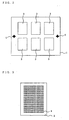
- FIG. 1 is an illustration showing a deposition mask according to a first embodiment of the present invention.
- FIG. 1(A) is a top view showing the deposition mask and
- FIG. 1(B) is a transverse sectional view showing the deposition mask.
- the deposition mask of the first embodiment has a configuration in which a plurality of mask chips 2 each including a single crystal silicon substrate are arranged on the upper face of a mask support 1 made of borosilicate glass, the number of the mask chips 2 being six in FIG. 1(a).
- the mask support 1 has a plurality of apertures 3 and the mask chips 2 are joined to the mask support 1 in such a manner that the mask chips 2 respectively cover the corresponding apertures 3.
- Each of the mask chip 2 has a large number of openings 4 corresponding to pixels.
- the openings 4 have a size of several ten- ⁇ m square and all single-color pixels are formed in one step when a deposition substrate is treated by a vapor deposition process.
- a method for forming electroluminescent layers by the vapor deposition process is described later in detail.
- the mask support 1 has convex alignment marks 5 used for aligning the mask support 1 with the deposition substrate (of positions and directions).
- the alignment marks 5 may be recessions or perforations.
- the mask support 1 is made of borosilicate glass; however, the mask support 1 may be formed of a silicon substrate. Furthermore, a single mask chip may be joined to mask support 1 instead of a plurality of the mask chips 2.
- FIG. 2 is an illustration showing the mask support 1 of the deposition mask shown in FIG. 1
- FIG. 3 is an illustration showing one of the mask chips 2 of the deposition mask shown in FIG. 1.
- the mask support 1 has a plurality of the apertures 3 and the alignment marks 5 are placed on the upper face thereof.
- the apertures 3 are formed, for example, by directing a jet of fine abrasive grains toward a borosilicate glass substrate.
- the alignment marks 5 may be formed according to the following procedure: a gold or chromium layer is formed on the borosilicate glass substrate by a sputtering process and the resulting substrate is patterned by a photolithographic process and then etched.
- the mask chips 2 each have a large number of the openings 4.
- the mask chips 2 are joined to the mask support 1 such that the openings 4 are positioned above the apertures 3.
- the mask support 1 is preferably prepared using a material having a thermal expansion coefficient close or equal to that of silicon. This is because heat strain can be prevented from being applied to joints between the mask support 1 and the mask chips 2 when an electroluminescent layer is formed by the vapor deposition process.
- borosilicate glass Pyrex TM #7744 manufactured by Corning Inc.
- silicon has a thermal expansion coefficient of 3.5 x 10 -6 / °C, that is, the thermal expansion coefficient of the glass is very close to that of silicon; hence, the glass is fit to prepare the mask support 1.
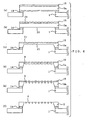
- FIG. 4 is an illustration showing a step of dividing a single crystal silicon wafer into single crystal silicon substrates for preparing the mask chips 2.
- the following wafer is prepared: a single crystal silicon wafer 10 having a surface of, for example, a ⁇ 100> crystal orientation and having two orientation flats 11 (hereinafter referred to as ori-flas).
- the single crystal silicon wafer 10 has the ⁇ 100> crystal orientation and the ori-flas 11 perpendicularly crossing each other in a ⁇ 100> crystal plane.
- the single crystal silicon wafer 10 is covered with a silicon dioxide layer, formed by thermal oxidation in advance, for forming an etching mask.
- the single crystal silicon wafer 10 is cut along lines parallel to the ori-flas 11 with a dicing saw, whereby the single crystal silicon substrates 2a having a rectangular shape are obtained.
- the single crystal silicon wafer 10 may be cloven into the single crystal silicon substrates 2a without using the dicing saw.
- narrow grooves are preferably formed along dividing lines in advance.
- the single crystal silicon substrates 2a need not be rectangular if the single crystal silicon substrates 2a each have at least one straight side.
- Silicon dioxide layers may be formed on the respective single crystal silicon substrates 2a after cutting the wafer, or silicon nitride layers or the like may be formed thereon with a CVD (Chemical Vapor Deposition) system.
- FIG. 5 is a top view showing a step of joining the single crystal silicon substrates 2a made by the process shown in FIG. 4 to the mask support 1.
- the single crystal silicon substrates 2a do not yet have the openings 4 corresponding to pixels.
- the mask chips 2 are joined to the upper face of the mask support 1 provided with the apertures 3 and the alignment marks 5.
- the crystal orientations of the single crystal silicon substrates 2a are aligned with each other using a reference member 12 having at least one straight side. In order to align the crystal orientations, the directions of the alignment marks 5 and the reference member 12 are relatively aligned and sides of the single crystal silicon substrates 2a obtained by the process shown in FIG.
- the single crystal silicon substrates 2a arranged in a line as shown in FIG. 5 can be joined to the mask support 1 in one step using the reference member 12.
- the alignment is herein performed for each line using the reference member 12.
- the single crystal silicon substrates 2a are joined to the mask support 1 with a UV-curable adhesive. Since the openings 4 corresponding to pixels are formed after the single crystal silicon substrates 2a are joined to the mask support 1 as described below, the accuracy of the positions of the single crystal silicon substrates 2a need not be so high.
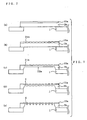
- FIG. 6 is an enlarged sectional view showing a step of processing the mask support 1 having the single crystal silicon substrates 2a preliminarily joined in the step shown in FIG. 5, to prepare the deposition mask.
- FIG. 6 shows one of the single crystal silicon substrates 2a and regions of the mask support 1 surrounding the substrate.
- the mask support 1 having the single crystal silicon substrates 2a joined in the step shown in FIG. 5 is prepared (FIG. 6(a)).
- silicon dioxide layers 15 are placed on both surfaces of each single crystal silicon substrate 2a, and the single crystal silicon substrate 2a is joined to the mask support 1 with the UV-curable adhesive 14.
- a silicon dioxide layer 20 placed on the lower face of the single crystal silicon substrate 2a is removed, and the silicon dioxide layer 15 placed on the upper face of the single crystal silicon substrate 2a is patterned by a photolithographic process, whereby a pattern corresponding to a pixel pattern (the openings 4) is formed.
- the resulting silicon dioxide layer 15 is then half-etched using hydrofluoric acid, whereby patterned portions 21 are formed (FIG. 6(b)).
- the silicon dioxide layer 20 placed on the lower face of the single crystal silicon substrate 2a is photolithographically processed and then dry-etched using CF 3 gas, whereby the silicon dioxide layer 20 is selectively removed.
- the mask support 1 having each single crystal silicon substrate 2a is immersed in an aqueous TMAH (tetramethyl hydroxide) solution, whereby the lower faces of the single crystal silicon substrate 2a is isotropically etched, thereby forming a recessed section 22.
- the resulting mask support 1 having the single crystal silicon substrate 2a is then immersed in an aqueous hydrofluoric acid solution, whereby the silicon dioxide layer 15 placed on the upper face of the single crystal silicon substrate 2a is etched until portions of the silicon dioxide layers 15 under the patterned portions 21 are entirely removed (FIG. 6(c)).
- Regions under the patterned portions 21 are then irradiated with YAG laser light, whereby the openings 4 are formed (FIG. 6(d)).
- the silicon dioxide layer 15 functions as a deposition mask; hence, only silicon portions are etched, whereby the openings 4 are formed in the single crystal silicon substrate 2a.
- the mask support 1 having the single crystal silicon substrates 2a is then immersed in an aqueous potassium hydroxide solution, whereby the single crystal silicon substrates 2a are anisotropically etched (FIG. 6(e)). According to this operation, silicon regions surrounding the openings 4 of the single crystal silicon substrate 2a are etched and therefore tapered off. This is because an evaporated material is allowed to pass through the openings 4 in various directions in a deposition step.
- the silicon dioxide layer 15 placed on the upper face of the single crystal silicon substrate 2a is removed by a dry etching process using the CF 3 gas, whereby the deposition mask is completed (FIG. 6(f)).
- the silicon dioxide layers 15 may be removed using a diluted aqueous hydrofluoric acid solution, in the step shown in FIG. 6(f).
- the deposition mask is completed in the step shown in FIG. 6(f).
- a thin film consisting of carbon and fluorine may be formed on the upper face of the obtained deposition mask.
- This film is referred to as a so-called Teflon TM film.
- Teflon TM film The deposition mask having the film can be readily detached from the deposition substrate in the vapor deposition step.
- the deposition mask is treated in a plasma atmosphere containing a mixture of carbon and fluorine, thereby forming the thin film to cover the deposition mask.
- the single crystal silicon substrates 2a are joined to the mask support 1 made of borosilicate glass and the openings 4 corresponding to a pixel pattern are then formed, the accuracy of the positions of the single crystal silicon substrates 2a joined to the mask support 1 need not be high; hence, the deposition mask can be easily prepared. Furthermore, since the openings 4 are formed after the single crystal silicon substrates 2a are joined to the mask support 1, the openings are fit to form the fine pixel pattern. Since a plurality of the single crystal silicon substrates are joined to the mask support, a large-sized deposition substrate can be treated by a vapor deposition process; hence, a large number of electroluminescent display units can be manufactured at a time.
- the crystal orientations of the single crystal silicon substrates 2a are aligned with each other using the reference member 12 having at least one straight side; hence, the single crystal silicon substrates 2a arranged in a line can be joined to the mask support 1 in one step. Furthermore, the crystal orientations of the single crystal silicon substrates 2a can be precisely aligned with each other by the use of the reference member 12.
- FIG. 7 is an enlarged sectional view showing steps of manufacturing a deposition mask according to a second embodiment of the present invention.
- FIG. 7 shows one of single crystal silicon substrates 2b and regions of a mask support surrounding the substrate.
- the deposition mask of the second embodiment has substantially the same configuration as that of the deposition mask of the first embodiment shown in FIG. 1 unless otherwise specified, and the same components as those of the deposition mask of the first embodiment shall have the same reference numerals.
- a gold-chromium layer 15a is formed by a sputtering process on the upper face of a single crystal silicon wafer 10, as shown in FIG. 4, having a ⁇ 100> crystal orientation.
- a chromium sub-layer having affinity for silicon is preferably formed primarily and a gold sub-layer having high chemical resistance is then formed thereon.
- the resulting single crystal silicon wafer 10 is cut into single crystal silicon substrates 2b and the single crystal silicon substrates 2b are then joined to the mask support 1 made of borosilicate glass by anodic coupling in the same manner as that described in the first embodiment (FIG. 7(a)).
- the single crystal silicon substrates 2b and the mask support 1 are first arranged so that the surfaces of the substrates meet the surface of the mask support 1, the crystal orientations of the substrates are subsequently aligned with each other in the same manner as that described in the first embodiment, the resulting single crystal silicon substrates 2b and mask support 1 are heated to 300°C to 500°C, and a voltage of about 500 V is then applied to them.
- the gold-chromium layer 15a of each substrate is then patterned, whereby a pattern corresponding to a pixel pattern (openings 4) is formed.
- the resulting layer is half-etched using an etching solution for gold and chromium, whereby patterned portions 21a are formed (FIG. 7(b)).
- each single crystal silicon substrates. 2b is anisotropically etched using an aqueous TMAH solution, whereby recessed sections 22a are formed.
- the resulting mask support 1 having the single crystal silicon substrate 2b is then immersed in the etching solution for gold and chromium, whereby the gold-chromium layer 15a is etched until the patterned portions 21a of the gold-chromium layer are entirely removed (FIG. 7(c)).
- the openings 4 are formed in the single crystal silicon substrate 2b by the application of YAG laser light in the same manner as that described in the first embodiment (FIG. 7(d)). Finally, the mask support 1 having the single crystal silicon substrate 2b is etched using an aqueous potassium hydroxide solution, whereby silicon regions surrounding the openings 4 of the single crystal silicon substrate 2b are tapered off, thereby obtaining the deposition mask (FIG. 7(e)).
- the gold-chromium layer 15a remaining in the step shown in FIG. 7(e) may be removed by an etching process.
- the single crystal silicon substrates 2b are joined to the mask support 1 made of borosilicate glass by anodic coupling, an adhesive is not necessary and flexure due to such an adhesive can be prevented from occurring. Furthermore, since no adhesive is used, no gases are formed in a vapor deposition step; hence, the deposition mask fit for high-vacuum deposition can be manufactured.
- FIG. 8 is a vertical sectional view showing one of pixels included in an electroluminescent display unit according to a third embodiment of the present invention.
- an organic EL display unit is described as an example of the electroluminescent display unit.
- the organic EL display unit shown in FIG. 8 includes a glass substrate 30 made of alkali-free glass, TFT wiring lines 31, a planarizing insulating layer 32, and an ITO layer 33 disposed in that order.
- ITO Indium Tin Oxide
- Silicon dioxide layer 34 is placed at regions, emitting no light, surrounding the pixel.
- a hole-transport layer 35, a light-emitting layer 36, and an electron-injection layer 37, which constitute an electroluminescent layer, are made of organic EL materials and formed by a vapor deposition process or the like.
- ITO layers 38 functioning as cathodes and a transparent sealing film 39 are disposed on these layers.
- the deposition mask described in the first or second embodiment is principally used for forming the electroluminescent layer, but it may be used as a sputter mask for forming the ITO layer 33 by a sputtering process.
- the electroluminescent layer may include a hole-injection layer or the like if it is provided in addition to the hole-transport layer 35, the light-emitting layer 36, and the electron-injection layer 37.
- an electron-transport layer, a light-emitting layer, and hole-injection layer functioning as an electroluminescent layer may be formed instead of the hole-transport layer 35, the light-emitting layer 36, and the electron-injection layer 37.
- FIG. 9 is a fragmentary sectional view showing steps of forming the electroluminescent layer using the deposition mask described in the first or second embodiment.
- Openings 4 of a deposition mask 40 (FIG. 9 shows periphery of the openings 4 only) are arranged to meet portions for red pixels on a glass substrate 30 having an ITO layer 33 and the like, and a red electroluminescent layer 51 for the red pixels are formed by a vapor deposition process (FIG. 9(a)).
- the deposition mask 40 is then moved so that the openings 4 are arranged to meet portions for green pixels on the glass substrate 30, and a green electroluminescent layer 52 for the green pixels are then formed by the vapor deposition process (FIG. 9(b)).
- a blue electroluminescent layer 53 for blue pixels are formed by the vapor deposition process (FIG. 9(c)).
- the electroluminescent layer is formed using the deposition mask described in the first or second embodiment, a high-definition electroluminescent display unit including the fine electroluminescent layer can be manufactured.
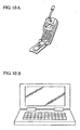
- FIG. 10 is an illustration showing an example of an electronic apparatus according to a fourth embodiment of the present invention.
- FIG. 10(A) shows a mobile phone including a display panel, which is an example of an electroluminescent display unit of the present invention.
- FIG. 10(B) shows a personal computer including the electroluminescent display unit of the present invention.
- the electroluminescent display unit of the present invention can be used for a display panel for a game machine or a digital camera.
Landscapes
- Chemical & Material Sciences (AREA)
- Engineering & Computer Science (AREA)
- Chemical Kinetics & Catalysis (AREA)
- Materials Engineering (AREA)
- Mechanical Engineering (AREA)
- Metallurgy (AREA)
- Organic Chemistry (AREA)
- Manufacturing & Machinery (AREA)
- Electroluminescent Light Sources (AREA)
- Physical Vapour Deposition (AREA)
- Liquid Crystal (AREA)
Claims (6)
- Procédé de fabrication d'un masque de dépôt comprenant une configuration dans laquelle une pluralité de puces de masque (2) chacune consistant en un substrat de silicium cristallin unique (2a) sont fixées par fusion à un support de masque (1) fait de verre de borosilicate, comprenant :une étape consistant à fixer par fusion la pluralité de puces de masque aux sections prédéterminées du support de masque (1) de sorte que l'orientation cristalline de chacune des puces de masque (2) soit alignée dans une direction prédéterminée, et une étape consistant à former des ouvertures (4) dans les puces de masque (2) fixées par fusion sur le support de masque,caractérisé en ce que l'étape de formation est réalisée après l'étape de fixation par fusion.
- Procédé selon la revendication 1, dans lequel l'étape de fixation par fusion de la pluralité de puces de masque aux sections prédéterminées au support de masque (1) comprend une sous-étape consistant à aligner l'orientation cristalline des puces de masque dans la direction prédéterminée en utilisant un organe de référence (12) ayant au moins un côté droit.
- Procédé selon la revendication 1 ou 2, comprenant en outre une étape consistant à former un masque de gravure sur les puces de masque, l'étape de formation du masque de gravure étant réalisée avant la réalisation de l'étape consistant à fixer par fusion les puces de masque (2) aux sections prédéterminées du support de masque (1).
- Procédé selon l'une quelconque des revendications 1 à 3, dans lequel les puces de masque (2) sont fixées par fusion au support de masque (1) par un couplage anodique.
- Procédé selon l'une quelconque des revendications 1 à 4, dans lequel les substrats de silicium cristallin uniques (2a) des puces de masque sont préparés en divisant une tranche de silicium cristallin unique (10) en utilisant le clivage.
- Procédé selon l'une quelconque des revendications 1 à 5, dans lequel les films fins consistant en du carbone et du fluor sont formés sur les surfaces des puces de masque (2), dans une atmosphère de plasma de mélange de carbone et fluor.
Applications Claiming Priority (2)
| Application Number | Priority Date | Filing Date | Title |
|---|---|---|---|
| JP2003200064 | 2003-07-22 | ||
| JP2003200064A JP2005042133A (ja) | 2003-07-22 | 2003-07-22 | 蒸着マスク及びその製造方法、表示装置及びその製造方法、表示装置を備えた電子機器 |
Publications (4)
| Publication Number | Publication Date |
|---|---|
| EP1500716A2 EP1500716A2 (fr) | 2005-01-26 |
| EP1500716A3 EP1500716A3 (fr) | 2005-03-02 |
| EP1500716B1 true EP1500716B1 (fr) | 2007-03-21 |
| EP1500716B9 EP1500716B9 (fr) | 2008-09-24 |
Family
ID=33487632
Family Applications (1)
| Application Number | Title | Priority Date | Filing Date |
|---|---|---|---|
| EP04013251A Expired - Lifetime EP1500716B9 (fr) | 2003-07-22 | 2004-06-04 | Méthode de fabrication d'un masque de dépôt |
Country Status (7)
| Country | Link |
|---|---|
| US (1) | US7074694B2 (fr) |
| EP (1) | EP1500716B9 (fr) |
| JP (1) | JP2005042133A (fr) |
| KR (1) | KR100683323B1 (fr) |
| CN (1) | CN1578563A (fr) |
| DE (1) | DE602004005382T2 (fr) |
| TW (1) | TWI244354B (fr) |
Cited By (1)
| Publication number | Priority date | Publication date | Assignee | Title |
|---|---|---|---|---|
| WO2020190444A1 (fr) * | 2019-03-15 | 2020-09-24 | Applied Materials, Inc. | Masque de dépôt et procédés de fabrication et d'utilisation d'un masque de dépôt |
Families Citing this family (30)
| Publication number | Priority date | Publication date | Assignee | Title |
|---|---|---|---|---|
| JP3775493B2 (ja) * | 2001-09-20 | 2006-05-17 | セイコーエプソン株式会社 | マスクの製造方法 |
| JP2005179742A (ja) * | 2003-12-19 | 2005-07-07 | Seiko Epson Corp | マスク、マスクの製造方法、有機エレクトロルミネッセンス装置の製造方法、有機エレクトロルミネッセンス装置、及び電子機器 |
| JP2005276480A (ja) * | 2004-03-23 | 2005-10-06 | Seiko Epson Corp | マスク、マスクの製造方法、薄膜パターンの形成方法、電気光学装置の製造方法および電子機器 |
| US7517558B2 (en) | 2005-06-06 | 2009-04-14 | Micron Technology, Inc. | Methods for positioning carbon nanotubes |
| KR100658762B1 (ko) * | 2005-11-30 | 2006-12-15 | 삼성에스디아이 주식회사 | 증착용 마스크 프레임 조립체 및 이를 이용한 증착 방법 |
| KR100754482B1 (ko) * | 2006-09-01 | 2007-09-03 | 엘지전자 주식회사 | 디스플레이 소자 제조용 마스크 |
| KR100759578B1 (ko) * | 2006-11-10 | 2007-09-18 | 삼성에스디아이 주식회사 | 유기 발광 표시장치 및 그 제조방법 |
| JP2008268666A (ja) * | 2007-04-23 | 2008-11-06 | Fujifilm Corp | 素子の製造方法及びそれを用いた表示装置の製造方法 |
| CN100472772C (zh) * | 2007-05-15 | 2009-03-25 | 日月光半导体制造股份有限公司 | 线路板与电路结构 |
| KR101029999B1 (ko) * | 2009-12-15 | 2011-04-20 | 삼성모바일디스플레이주식회사 | 마스크, 마스크 제조 방법 및 마스크 제조 장치 |
| KR101107159B1 (ko) * | 2009-12-17 | 2012-01-25 | 삼성모바일디스플레이주식회사 | 평판 표시장치의 박막 증착용 마스크 조립체 |
| KR101232181B1 (ko) | 2010-02-03 | 2013-02-12 | 엘지디스플레이 주식회사 | 마스크 어셈블리 |
| KR101783456B1 (ko) * | 2012-06-22 | 2017-10-10 | 주식회사 원익아이피에스 | 증착장치용 마스크, 마스크와 기판의 정렬방법, 및 기판 상 물질층 형성방법 |
| JP6142386B2 (ja) * | 2012-12-21 | 2017-06-07 | 株式会社ブイ・テクノロジー | 蒸着マスクの製造方法 |
| CN103236398B (zh) * | 2013-04-19 | 2015-09-09 | 深圳市华星光电技术有限公司 | 光罩掩模板的制作方法及用该方法制作的光罩掩模板 |
| CN107346803A (zh) * | 2016-05-05 | 2017-11-14 | 上海珏芯光电科技有限公司 | 硅基背板led显示器的制造方法 |
| CN105839052A (zh) | 2016-06-17 | 2016-08-10 | 京东方科技集团股份有限公司 | 掩膜板以及掩膜板的组装方法 |
| CN106435473A (zh) * | 2016-11-11 | 2017-02-22 | 京东方科技集团股份有限公司 | 掩模板及其制作方法、有机发光二极管显示器的制作方法 |
| JP7121918B2 (ja) * | 2016-12-14 | 2022-08-19 | 大日本印刷株式会社 | 蒸着マスク装置及び蒸着マスク装置の製造方法 |
| WO2018110253A1 (fr) * | 2016-12-14 | 2018-06-21 | 大日本印刷株式会社 | Dispositif de masque de dépôt en phase vapeur et procédé de fabrication de dispositif de masque de dépôt en phase vapeur |
| CN106884140B (zh) * | 2017-04-28 | 2019-04-30 | 京东方科技集团股份有限公司 | 一种掩膜组件及其组装方法 |
| CN107099770B (zh) * | 2017-06-08 | 2020-03-06 | 京东方科技集团股份有限公司 | 掩膜板、其制作方法和利用其进行蒸镀方法 |
| JP6998139B2 (ja) * | 2017-06-28 | 2022-01-18 | 株式会社ジャパンディスプレイ | 蒸着マスク |
| CN107761049A (zh) * | 2017-10-09 | 2018-03-06 | 深圳市华星光电半导体显示技术有限公司 | 蒸镀用uv前处理设备 |
| CN108123067B (zh) * | 2017-11-16 | 2019-05-31 | 上海视涯信息科技有限公司 | 一种荫罩及其制造方法 |
| TWI826497B (zh) * | 2018-08-09 | 2023-12-21 | 南韓商Tgo科技股份有限公司 | 遮罩支撑模板與其製造方法及框架一體型遮罩的製造方法 |
| JP7749925B2 (ja) * | 2020-03-13 | 2025-10-07 | 大日本印刷株式会社 | 有機デバイスの製造装置の蒸着室の評価方法 |
| US11638388B2 (en) * | 2020-05-15 | 2023-04-25 | The Hong Kong University Of Science And Technology | High-resolution shadow masks |
| KR102929156B1 (ko) * | 2020-08-31 | 2026-02-24 | 삼성디스플레이 주식회사 | 마스크, 이의 제조 방법, 및 표시 패널 제조 방법 |
| JP7589010B2 (ja) * | 2020-10-28 | 2024-11-25 | キヤノン株式会社 | 蒸着マスク、蒸着マスクを用いたデバイスの製造方法 |
Family Cites Families (14)
| Publication number | Priority date | Publication date | Assignee | Title |
|---|---|---|---|---|
| JP2634714B2 (ja) | 1991-08-05 | 1997-07-30 | 信越化学工業株式会社 | X線マスク構造体の製造方法 |
| US5538151A (en) | 1995-01-20 | 1996-07-23 | International Business Machines Corp. | Recovery of an anodically bonded glass device from a susstrate by use of a metal interlayer |
| DE69622277T2 (de) * | 1995-09-18 | 2003-03-27 | Hitachi, Ltd. | Halbleitermaterial, verfahren zur herstellung des halbleitermaterials und eine halbleitervorrichtung |
| JPH1021586A (ja) | 1996-07-02 | 1998-01-23 | Sony Corp | Dcスパッタリング装置 |
| JP3420675B2 (ja) * | 1996-12-26 | 2003-06-30 | シャープ株式会社 | 液晶表示装置およびその製造方法 |
| JPH10207044A (ja) | 1997-01-24 | 1998-08-07 | Toppan Printing Co Ltd | 荷電ビーム露光用透過マスク |
| JP2001185350A (ja) | 1999-12-24 | 2001-07-06 | Sanyo Electric Co Ltd | 被着用マスク、その製造方法、エレクトロルミネッセンス表示装置及びその製造方法 |
| JP2002220656A (ja) | 2000-11-22 | 2002-08-09 | Sanyo Electric Co Ltd | 蒸着用マスクおよびその製造方法 |
| JP4092914B2 (ja) | 2001-01-26 | 2008-05-28 | セイコーエプソン株式会社 | マスクの製造方法、有機エレクトロルミネッセンス装置の製造方法 |
| JP2003007597A (ja) * | 2001-06-25 | 2003-01-10 | Canon Inc | マスクパターン偏倍方法、偏倍装置及びマスク構造体 |
| JP2003022987A (ja) * | 2001-07-09 | 2003-01-24 | Sanyo Electric Co Ltd | 化合物半導体装置の製造方法 |
| JP3596502B2 (ja) | 2001-09-25 | 2004-12-02 | セイコーエプソン株式会社 | マスク及びその製造方法、エレクトロルミネッセンス装置及びその製造方法並びに電子機器 |
| JP3651432B2 (ja) | 2001-09-25 | 2005-05-25 | セイコーエプソン株式会社 | マスク及びその製造方法並びにエレクトロルミネッセンス装置の製造方法 |
| US20030151118A1 (en) | 2002-02-14 | 2003-08-14 | 3M Innovative Properties Company | Aperture masks for circuit fabrication |
-
2003
- 2003-07-22 JP JP2003200064A patent/JP2005042133A/ja active Pending
-
2004
- 2004-05-26 US US10/854,779 patent/US7074694B2/en not_active Expired - Lifetime
- 2004-06-04 DE DE602004005382T patent/DE602004005382T2/de not_active Expired - Lifetime
- 2004-06-04 EP EP04013251A patent/EP1500716B9/fr not_active Expired - Lifetime
- 2004-07-14 TW TW093121038A patent/TWI244354B/zh not_active IP Right Cessation
- 2004-07-16 CN CNA2004100716272A patent/CN1578563A/zh active Pending
- 2004-07-21 KR KR1020040056707A patent/KR100683323B1/ko not_active Expired - Lifetime
Cited By (2)
| Publication number | Priority date | Publication date | Assignee | Title |
|---|---|---|---|---|
| WO2020190444A1 (fr) * | 2019-03-15 | 2020-09-24 | Applied Materials, Inc. | Masque de dépôt et procédés de fabrication et d'utilisation d'un masque de dépôt |
| US11631813B2 (en) | 2019-03-15 | 2023-04-18 | Applied Materials, Inc. | Deposition mask and methods of manufacturing and using a deposition mask |
Also Published As
| Publication number | Publication date |
|---|---|
| KR20050011704A (ko) | 2005-01-29 |
| KR100683323B1 (ko) | 2007-02-15 |
| US7074694B2 (en) | 2006-07-11 |
| EP1500716A2 (fr) | 2005-01-26 |
| JP2005042133A (ja) | 2005-02-17 |
| TWI244354B (en) | 2005-11-21 |
| TW200509738A (en) | 2005-03-01 |
| EP1500716A3 (fr) | 2005-03-02 |
| EP1500716B9 (fr) | 2008-09-24 |
| DE602004005382D1 (de) | 2007-05-03 |
| CN1578563A (zh) | 2005-02-09 |
| DE602004005382T2 (de) | 2007-11-29 |
| US20050019968A1 (en) | 2005-01-27 |
Similar Documents
| Publication | Publication Date | Title |
|---|---|---|
| EP1500716B1 (fr) | Méthode de fabrication d'un masque de dépôt | |
| US7268406B2 (en) | Mask, mask chip, manufacturing method of mask, manufacturing method of mask chip, and electronic device | |
| US6118502A (en) | Using a temporary substrate to attach components to a display substrate when fabricating a passive type display device | |
| US6815240B2 (en) | Thin film semiconductor device and manufacturing method thereof | |
| CN100428527C (zh) | 掩模及其制法、场致发光装置及其制法以及电子机器 | |
| US6459193B1 (en) | Shadow mask, a method of forming the shadow mask, and a method of manufacturing a semiconductor device with using the shadow mask | |
| US20020111035A1 (en) | System and methods for manufacturing and using a mask | |
| KR20060134934A (ko) | 액티브 매트릭스 디스플레이 및 플라스틱 기판을 구비하는다른 전자 장치 | |
| US7033665B2 (en) | Precision mask for deposition and a method for manufacturing the same, an electroluminescence display and a method for manufacturing the same, and electronic equipment | |
| JPH08254686A (ja) | 表示装置の作製方法 | |
| KR20060045140A (ko) | 마스크, 마스크의 제조 방법, 전기 광학 장치의 제조 방법및 전자기기 | |
| JP2003347524A (ja) | 素子の転写方法、素子の配列方法及び画像表示装置の製造方法 | |
| US6965424B2 (en) | Method of preventing seal damage in LCD panel manufacturing | |
| JP3550027B2 (ja) | 平面型表示パネルの製造方法 | |
| WO2024162227A1 (fr) | Masque à cadre et procédé de fabrication de dispositif organique | |
| JP5176260B2 (ja) | 画像表示装置の製造方法 | |
| JP2004213992A (ja) | 表示装置用素子基板の製造方法及び転写体 | |
| JP2006077276A (ja) | マスク、マスクの製造方法、薄膜パターンの形成方法、電気光学装置の製造方法 | |
| JP2025136535A (ja) | フレーム付きマスク、剥離層付きマスク、剥離層付きフレーム、マスクの交換方法、及び、有機デバイスの製造方法 | |
| JPH08254692A (ja) | 液晶表示パネルおよびその製造方法 | |
| JP2024107752A (ja) | フレーム付きマスク、及び、有機デバイスの製造方法 | |
| JP2006077297A (ja) | マスク、成膜方法、有機el装置の製造方法 | |
| CN119422469A (zh) | 成膜装置、成膜方法及电子器件的制造方法 | |
| JP2008231497A (ja) | 成膜用マスク部材、および成膜用マスク部材の製造方法 | |
| JPH03259124A (ja) | 薄膜トランジスタマトリクスの製造方法 |
Legal Events
| Date | Code | Title | Description |
|---|---|---|---|
| PUAI | Public reference made under article 153(3) epc to a published international application that has entered the european phase |
Free format text: ORIGINAL CODE: 0009012 |
|
| PUAL | Search report despatched |
Free format text: ORIGINAL CODE: 0009013 |
|
| 17P | Request for examination filed |
Effective date: 20040604 |
|
| AK | Designated contracting states |
Kind code of ref document: A2 Designated state(s): AT BE BG CH CY CZ DE DK EE ES FI FR GB GR HU IE IT LI LU MC NL PL PT RO SE SI SK TR |
|
| AX | Request for extension of the european patent |
Extension state: AL HR LT LV MK |
|
| AK | Designated contracting states |
Kind code of ref document: A3 Designated state(s): AT BE BG CH CY CZ DE DK EE ES FI FR GB GR HU IE IT LI LU MC NL PL PT RO SE SI SK TR |
|
| AX | Request for extension of the european patent |
Extension state: AL HR LT LV MK |
|
| AKX | Designation fees paid |
Designated state(s): DE FR GB |
|
| RTI1 | Title (correction) |
Free format text: MANUFACTURING METHOD OF A DEPOSITION MASK |
|
| GRAP | Despatch of communication of intention to grant a patent |
Free format text: ORIGINAL CODE: EPIDOSNIGR1 |
|
| GRAS | Grant fee paid |
Free format text: ORIGINAL CODE: EPIDOSNIGR3 |
|
| GRAA | (expected) grant |
Free format text: ORIGINAL CODE: 0009210 |
|
| AK | Designated contracting states |
Kind code of ref document: B1 Designated state(s): DE FR GB |
|
| REG | Reference to a national code |
Ref country code: GB Ref legal event code: FG4D |
|
| REF | Corresponds to: |
Ref document number: 602004005382 Country of ref document: DE Date of ref document: 20070503 Kind code of ref document: P |
|
| ET | Fr: translation filed | ||
| PLBE | No opposition filed within time limit |
Free format text: ORIGINAL CODE: 0009261 |
|
| STAA | Information on the status of an ep patent application or granted ep patent |
Free format text: STATUS: NO OPPOSITION FILED WITHIN TIME LIMIT |
|
| 26N | No opposition filed |
Effective date: 20071227 |
|
| REG | Reference to a national code |
Ref country code: DE Ref legal event code: R082 Ref document number: 602004005382 Country of ref document: DE Representative=s name: HOFFMANN, ECKART, DIPL.-ING., DE |
|
| REG | Reference to a national code |
Ref country code: DE Ref legal event code: R082 Ref document number: 602004005382 Country of ref document: DE Representative=s name: HOFFMANN, ECKART, DIPL.-ING., DE Effective date: 20130807 Ref country code: DE Ref legal event code: R081 Ref document number: 602004005382 Country of ref document: DE Owner name: INTELLECTUAL KEYSTONE TECHNOLOGY LLC, US Free format text: FORMER OWNER: SEIKO EPSON CORP., TOKYO, JP Effective date: 20130807 Ref country code: DE Ref legal event code: R081 Ref document number: 602004005382 Country of ref document: DE Owner name: INTELLECTUAL KEYSTONE TECHNOLOGY LLC, WILMINGT, US Free format text: FORMER OWNER: SEIKO EPSON CORP., TOKYO, JP Effective date: 20130807 |
|
| REG | Reference to a national code |
Ref country code: FR Ref legal event code: TP Owner name: INTELLECTUAL KEYSTONE TECHNOLOGY LLC, US Effective date: 20130827 |
|
| REG | Reference to a national code |
Ref country code: GB Ref legal event code: 732E Free format text: REGISTERED BETWEEN 20130919 AND 20130925 |
|
| REG | Reference to a national code |
Ref country code: FR Ref legal event code: PLFP Year of fee payment: 13 |
|
| REG | Reference to a national code |
Ref country code: FR Ref legal event code: PLFP Year of fee payment: 14 |
|
| REG | Reference to a national code |
Ref country code: FR Ref legal event code: PLFP Year of fee payment: 15 |
|
| PGFP | Annual fee paid to national office [announced via postgrant information from national office to epo] |
Ref country code: FR Payment date: 20230522 Year of fee payment: 20 Ref country code: DE Payment date: 20230522 Year of fee payment: 20 |
|
| PGFP | Annual fee paid to national office [announced via postgrant information from national office to epo] |
Ref country code: GB Payment date: 20230523 Year of fee payment: 20 |
|
| REG | Reference to a national code |
Ref country code: DE Ref legal event code: R071 Ref document number: 602004005382 Country of ref document: DE |
|
| REG | Reference to a national code |
Ref country code: GB Ref legal event code: PE20 Expiry date: 20240603 |
|
| PG25 | Lapsed in a contracting state [announced via postgrant information from national office to epo] |
Ref country code: GB Free format text: LAPSE BECAUSE OF EXPIRATION OF PROTECTION Effective date: 20240603 |
|
| PG25 | Lapsed in a contracting state [announced via postgrant information from national office to epo] |
Ref country code: GB Free format text: LAPSE BECAUSE OF EXPIRATION OF PROTECTION Effective date: 20240603 |