EP1503328B1 - Source de photon unique - Google Patents
Source de photon unique Download PDFInfo
- Publication number
- EP1503328B1 EP1503328B1 EP03254736A EP03254736A EP1503328B1 EP 1503328 B1 EP1503328 B1 EP 1503328B1 EP 03254736 A EP03254736 A EP 03254736A EP 03254736 A EP03254736 A EP 03254736A EP 1503328 B1 EP1503328 B1 EP 1503328B1
- Authority
- EP
- European Patent Office
- Prior art keywords
- photon
- layer
- vertical cavity
- cavity structure
- charge
- Prior art date
- Legal status (The legal status is an assumption and is not a legal conclusion. Google has not performed a legal analysis and makes no representation as to the accuracy of the status listed.)
- Expired - Lifetime
Links
Images









Classifications
-
- B—PERFORMING OPERATIONS; TRANSPORTING
- B82—NANOTECHNOLOGY
- B82Y—SPECIFIC USES OR APPLICATIONS OF NANOSTRUCTURES; MEASUREMENT OR ANALYSIS OF NANOSTRUCTURES; MANUFACTURE OR TREATMENT OF NANOSTRUCTURES
- B82Y10/00—Nanotechnology for information processing, storage or transmission, e.g. quantum computing or single electron logic
-
- G—PHYSICS
- G02—OPTICS
- G02B—OPTICAL ELEMENTS, SYSTEMS OR APPARATUS
- G02B6/00—Light guides; Structural details of arrangements comprising light guides and other optical elements, e.g. couplings
- G02B6/10—Light guides; Structural details of arrangements comprising light guides and other optical elements, e.g. couplings of the optical waveguide type
- G02B6/12—Light guides; Structural details of arrangements comprising light guides and other optical elements, e.g. couplings of the optical waveguide type of the integrated circuit kind
- G02B6/122—Basic optical elements, e.g. light-guiding paths
- G02B6/1225—Basic optical elements, e.g. light-guiding paths comprising photonic band-gap structures or photonic lattices
-
- H—ELECTRICITY
- H04—ELECTRIC COMMUNICATION TECHNIQUE
- H04B—TRANSMISSION
- H04B10/00—Transmission systems employing electromagnetic waves other than radio-waves, e.g. infrared, visible or ultraviolet light, or employing corpuscular radiation, e.g. quantum communication
- H04B10/70—Photonic quantum communication
-
- H—ELECTRICITY
- H04—ELECTRIC COMMUNICATION TECHNIQUE
- H04L—TRANSMISSION OF DIGITAL INFORMATION, e.g. TELEGRAPHIC COMMUNICATION
- H04L9/00—Cryptographic mechanisms or cryptographic arrangements for secret or secure communications; Network security protocols
- H04L9/08—Key distribution or management, e.g. generation, sharing or updating, of cryptographic keys or passwords
- H04L9/0816—Key establishment, i.e. cryptographic processes or cryptographic protocols whereby a shared secret becomes available to two or more parties, for subsequent use
- H04L9/0852—Quantum cryptography
- H04L9/0858—Details about key distillation or coding, e.g. reconciliation, error correction, privacy amplification, polarisation coding or phase coding
-
- H—ELECTRICITY
- H04—ELECTRIC COMMUNICATION TECHNIQUE
- H04L—TRANSMISSION OF DIGITAL INFORMATION, e.g. TELEGRAPHIC COMMUNICATION
- H04L2209/00—Additional information or applications relating to cryptographic mechanisms or cryptographic arrangements for secret or secure communication H04L9/00
- H04L2209/34—Encoding or coding, e.g. Huffman coding or error correction
Definitions
- the present invention relates to a photon source for emitting photons singly or in pairs.
- the present invention also relates to a quantum computer.
- quantum information processing and quantum communication applications such as quantum cryptography and quantum teleportation, require a controllable stream of single photons or entangled pairs of photons.
- a sequence of polarized photons may be employed for distributing a key for use in encryption.
- the aim of key distribution is for the parties, which by convention are referred to as Alice and Bob, to arrive at a key which is known to them, but not an eavesdropper, Eve.
- a well-known key distribution scheme is the Bennett and Brassard protocol (usually referred to as the "BB84 protocol"), wherein Alice and Bob communicate through two communications channels: a classical channel and a quantum channel.
- the BB84 protocol comprises the following steps:
- Alice prepares a sequence of photons, each of which is randomly chosen to be in one of four different polarizations, namely 0° ( ⁇ ), 90° ( ⁇ ), 45° ( ) or 135° ( ). She uses a photon source to generate photons and a rotator to produce photons of the required polarization.
- Alice sends the sequence of photons to Bob through the quantum channel, which is may be air or an optical fibre.
- Alice may send a photon sequence comprising:
- Bob For each photon, Bob randomly picks a rectilinear ( ) or diagonal ( ) basis for performing a measurement. Typically, this involves using a polarization splitter and a photon detector. For instance, Bob may pick:
- the results may be:
- the classical channel may be a wired or wireless communications channel.
- Alice tells Bob whether he has chosen the correct basis for performing the measurement.
- Alice declares (using Y for "yes” and N for "no"):
- the polarization data can then be interpreted as a binary sequence according to a coding scheme.
- Alice and Bob test for eavesdropping by publicly comparing polarization data of a predetermined selection of photons on which they think they should agree. If they find no or few discrepancies, i.e. that there is low bit error rate, then they can infer that little information is known to Eve. Alice and Bob may then use the remaining data to form a key.
- Quantum cryptography An overview of quantum cryptography is found in "Quantum Cryptology” by Hoi-Kwong Lo, pp.76 to 119 of “Introduction to Quantum Computation and Information” ed. Hoi-Kwong Lo, Tim Spiller and Sanduffy (World Scientific Publishing, 1998). Experimental quantum cryptography systems are described in “Experimental Quantum Cryptography” by Hugo Zbinden, pp. 120 to 142 of “Introduction to Quantum Computation and Information” ibid.
- a pair of entangled photons can be used to teleport a photon.
- a photon source generates an entangled pair of photons which are transmitted through air or an optical fibre to Alice and Bob.
- the state of the entangled pair of photons may be described as:
- ⁇ ⁇ AB 2 - 1 ⁇ 2 ⁇
- Alice also has an additional photon C which she wishes to teleport to Bob. Alice may have another photon source or use one half of another entangled pair of photons.
- the additional photon is in a state
- ⁇ ⁇ C ⁇ ⁇
- Alice performs a so-called Bell-state measurement by combining her entangled and additional photons so that they lose their individuality and measuring the state of the combined pair in such a way that that the state of any one of the combined pair is not measured.
- This may be achieved by arranging for the photons strike opposite sides of a beam splitter at the same time so that their transmitted and reflected parts interfere.
- the overall state may be expressed in terms of the Bell states of the combined photons C, A:
- ⁇ ⁇ AB 1 ⁇ 2 ⁇
- ⁇ ⁇ B
- Quantum teleportation of a photon may be used for interfacing quantum computers.
- Quantum teleportation is described in more detail in "Quantum Information and Its Properties” by Richard Josza, pp. 49 to 75 of “Introduction to Quantum Computation and Information” ibid.
- An overview of quantum teleportation is given “Quantum Teleportation” by Anton Zielinger, pp. 32 to 41, Scientific American (April 2000).
- a photon source should produce a steady stream of photons (or entangled photon pairs) which can be divided into "pulse" windows of fixed duration, each pulse window containing one -and only one- photon.
- a photon source is still useful if, in each pulse window, there is a vanishingly small probability of finding two photons and only a small probability of finding no photons.
- Known single photon sources involve gating and attenuating conventional light sources, such as light-emitting diodes and lasers, and an example is described in Section III.A of "Quantum cryptography" by Nicolas Gisin, Grégoire Ribordy, Wolfganf Tittel and Hugo Zbinden, Reviews of Modern Physics, volume 74, pp. 145 to 190 (2002).
- these types of sources have drawbacks.
- Photon emission is random and described by Poisson statistics.
- the stream of photons is attenuated.
- the probability of finding no photons in a pulse window is increased. This ultimately results in slow information transfer.
- Known entangled-photon pair sources generally employ parametric downconversion and an example is also described in "Quantum cryptography” ibid..
- single photon emission from quantum dots controlled by optical pumping is described in "Quantum dots break new ground” by P. Michler, pages 27-28, Physics World (March 2002) and single photon emission from quantum dots controlled by electrical pumping is described in “Electrically Driven Single-Photon Source” by Z. Yuan et al ., Science, volume 235, pp. 102-105 (2002).
- Single photon emission from single molecules is disclosed in "Single photons on demand from a single molecule at room temperature” by B. Lounis and W. E. Moerner, Nature, volume 407, pp. 491-493 (2000).
- a single photon turnstile device in which photon emission is regulated by electron transfer is described in "A single-photon turnstile device" by J. Kim, O. Benson, H. Kan & Y. Yamamoto, Nature, volume 397, pp. 500-503 (1999).
- US-A- 2002196827 describes a photon source comprising a quantum dot having a confined conduction band energy level capable of being populated with at least one carrier and a confined valence band energy level capable of being populated by at least one carrier.
- the source further comprises supply means for intermittently supplying at least one carrier to the energy levels to create an exciton in the quantum dot, wherein the supply means are configured to regulate the supply of carriers such that as the exciton decays either a single photon or a plurality of single photons each having different distinct energies are emitted during a predetermined time interval.
- the photon source can include holes etched into a distributed Bragg reflector to provide a photonic bandgap structure.
- the present invention seeks to provide an improved photon source.
- a photon source for emitting photons singly or in pairs as specified in claim 1.
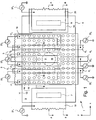
- the photon source 1 comprises a photon generation region 2, means 3 for controllably introducing a charge-carrier into the photon generation region 2 and means 4 for providing optical control over the photon generation region 2.
- the photon generation region 2 which in this example is a quantum dot formed in intrinsic gallium arsenide (GaAs), is embedded in a vertical cavity structure 5, which will be described in more detail later.
- GaAs intrinsic gallium arsenide
- the charge-carrier introducing means 3 includes a charge-carrier turnstile 6 disposed between source and drain terminals 7, 8.
- the source and drain terminals 7, 8 contact top and bottom contact layers 9, 10 respectively of the vertical cavity structure 5.
- a channel 11 is formed between source and drain terminals 7, 8.
- the charge-carrier turnstile 6 comprises a plurality of sets of gates 6 1 , 6 2 , 6 3 disposed on the vertical cavity structure 5.
- there are first, second and third sets of gates 6 1 , 6 2 , 6 3 each set of gates 6 1 , 6 2 , 6 3 comprising a pair of surface gates arranged in a split-gate configuration.
- the sets of gates 6 1 , 6 2 , 6 3 are offset from one another along the channel (along the x-axis) by a length s, preferably of the order of 0.1 or 1 ⁇ m.
- the gates within a pair of gates 6 1 , 6 2 , 6 3 are separated by a gap w 1 , w 2 , w 3 (along the y-axis), preferably of the order of 0.1 or 1 ⁇ m.
- gaps w 1 , w 3 for the first and second set of gates 6 1 , 6 3 are smaller than the gap w 2 for the second set of gates 6 2 .
- This arrangement helps to define the photon generation region 2 in the channel 11 between the second set of gates 6 2 .
- a single-electron turnstile is used 6 1 , 6 2 , 6 3 .
- the charge-carrier turnstile 6 may be used as a current pump as described in "Electron pump current by two pulses with phase delay" by K. Tsugagoshi and K. Nakazato, Applied Physics Letters, volume 71, pp. 3138-3140 (1997).
- the gates 6 1 , 6 2 , 6 3 deplete charge-carriers from regions of vertical cavity structure 5 lying beneath and adjacent to the gates. For example, if a sufficiently large gate bias is applied to the first set of gates 6 1 , then a depletion region 12 extends between the first set of gates 6 1 and across the channel 11, so as to pinch-off the channel 11.
- the optical control providing means 4 includes a photonic crystal structure 13, which may also be referred to as a photonic band-gap material.
- a two-dimensional photonic crystal structure is used which comprises a lattice of holes 14, preferably cylindrical, etched into the surface of the vertical cavity structure 5. Holes 14 based on polygons or ellipses may also be used.
- the holes 14 are filled with dielectric material 15, preferably polyimide.
- the holes 14 have a diameter ⁇ of the order of 10nm to 1 ⁇ m, preferably about 100nm.
- a square lattice is used, with a lattice constant a preferably of the order of 10nm to 1 ⁇ m.
- a defect 16 in this example a region in which lattice sites lack holes 14, is disposed within the photonic crystal structure 13.
- the defect 16 is for creating an optical defect state, which will be described in more detail later.
- An alternative photonic crystal structure may comprise a lattice of cylindrical pillars, which may be planarised with a dielectric.
- the optical control providing means 4 may optionally include magnetic field generating means 17 1 , 17 2 , 17 3 ,
- the magnetic field generating means 17 1 , 17 2 , 17 3 comprise respective variable magnetic field generating means 17 1 , 17 2 , 17 3 in the form of coils.
- static magnetic field generating means for example in the form of a nano- or micro-magnets, may be also be used. Both static and variable magnetic field generating means may be used to provide a static magnetic field in one region of the device and a variable magnetic field in another part of the device.
- the magnetic field generating means 17 1 , 17 2 , 17 3 are disposed on a dielectric 18 which overlies the vertical cavity structure 5.
- magnetic field generating means 17 1 , 17 2 , 17 3 may be embedded within dielectric 18. Nano or micro-magnets may be placed directly on the vertical cavity structure 5.
- Source and drain leads 19, 20 are connected to the source and drain terminals 7, 8.
- First and second voltage sources 21 1 , 21 2 are used to apply a bias across the source 7 and drain 8 respectively.
- the first and second voltage sources 20 1 , 20 2 may be replaced by a single voltage source (not shown).
- Third, fourth and fifth voltage sources 22 1 , 22 2 , 22 3 are used to apply biases to the first, second and third sets of gates 6 1 , 6 2 , 6 3 respectively.
- the third, fourth and fifth voltage sources 22 1 , 22 2 , 22 3 are programmable sources or variable frequency sources which allow high-frequency signals, for example of the order or 1 to 100 MHz, to be applied.
- a single voltage source (not shown) and a phase-offset circuit may be used.
- Sixth, seventh and eighth voltage sources 23 1 , 23 2 , 23 3 are used to drive a current through coils 17 1 , 17 2 , 17 3 respectively.
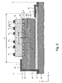
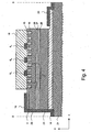
- the vertical cavity structure 5 is placed on a substrate 24 and comprises the bottom contact layer 10, an overlying lower mirror layer 25, an overlying lower cladding layer 26, an overlying active layer 27 which includes the photon generation region 2, an overlying upper cladding layer 28, an overlying upper mirror layer 29 and the top contact layer 9.
- the substrate 24 comprises semi-insulating gallium arsenide (GaAs).
- the bottom contact layer 10 comprises n-type GaAs, doped with silicon (Si) to a concentration of 2 ⁇ 10 18 cm -3 and having a thickness of 200nm.
- the active layer 27 comprises intrinsic GaAs having a thickness of 601 ⁇ .
- the top contact layer 9 comprises p-type GaAs, doped with C to a concentration of 2 ⁇ 10 18 cm -3 and having a thickness of 20nm.
- the etched holes 14 penetrate about 1 ⁇ m into the vertical cavity structure 5 (along the -z-axis) as shown by the arrow d and are filled with dielectric 15, such as polyimide.
- dielectric 15 such as polyimide.
- Other dielectrics may be used, such as an optical resist, silicon dioxide or silicon nitride. The dielectric is used to tune refractive index offset.
- the etched holes 14 may deeper, for example reaching active layer 27.
- the vertical cavity structure 5 is partially covered by an overlying dielectric layer 18 comprising polyimide and has a thickness of about 1 ⁇ m.
- the coils 17 1 , 17 2 , 17 3 are disposed on the dielectric layer 18 and comprise chromium/gold (Cr/Au) metallisations, the Cr layer having thickness of 10 nm and the Au layer having a thickness of 50 nm.
- the source and drain terminals 7, 8 comprise alloyed tin (Sn) ohmic contacts, having a pre-alloying thickness of 50nm, and chromium/gold (Cr/Au) metallisation, the Cr layer having thickness of 10 nm and the Au layer having a thickness of 50 nm.
- source and drain terminals 7, 8 may comprise a ferromagnetic material such as Cobalt (Co).
- the gates 6 1 , 6 2 , 6 3 overlie unetched portions of the top contact layer 9 and dielectric 15 filling holes 14.
- the charge-carrier introducing means 3 and optical control providing means 4 are arranged so as to control emission of photons 30 at a given rate and of a given configuration from the photon emission region 2, as will now be described in more detail:
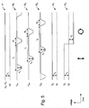
- signal waveform plots 31, 32 1 , 32 2 , 32 3 , 33 1 , 33 3 of voltages applied between the source and drain terminals 7, 8, between each of the sets of gates 6 1 , 6 2 , 6 3 and ground, and across the first and third coils 17 1 , 17 3 respectively are shown.
- the constant bias V 1 is greater than the electronic band gap of the active channel material, which in this case is GaAs, and is about 1.45V. This may be found by routine experiment.
- the constant bias V 1 is used to populate the quantum dot 2 with holes.
- a train of voltage pulses each pulse having a magnitude
- the pulse V 2 is sufficiently large that the depletion region 12 ( Figure 4) extends downwards to at least the depth of the lower cladding layer 26 ( Figure 4) and also laterally to pinch-off the channel 11 ( Figure 4).
- a voltage of the order of 1V is needed, although this may be found by routine experiment
- Each pulse has a duration ⁇ t 1 , ⁇ t 2 , ⁇ t 3 which is greater than photon emission times ⁇ , i.e.
- the photon emission time ⁇ depends on a number of factors including hole density, material, configuration of cavity, although typically it is of the order of 100 ps.
- Each train of voltages pulses has a pulse period ⁇ t 1 , ⁇ t 2 , ⁇ t 3 chosen according to the required photon emission rate. For example, a pulse period may be of the order of 10 ns.
- a bias V 3 is applied by the sixth voltage source 23, across the first coil 17 1 so as to drive a current I through the first coil 17 1 and generate a magnetic field between the source 7 and the photon generation region 2. This is to help introduce charge carriers into the photon generation region 2 of a given spin.
- the current I may be driven in a first or second sense, for example anti-clockwise or clockwise, to generate a magnetic field in a first or a second direction respectively, for example upwards (B ⁇ ) or downwards (B ⁇ ), in other words parallel or anti-parallel to the z-axis.
- a bias V 3' which may be substantially the same as V 3 , is applied by the eighth voltage source 23 3 across the third coil 17 2 so as to drive a current I through the third coil 17 3 and generate another magnetic field.
- the current I may be driven in the first or second sense to generate a magnetic field in the first or second directions respectively.
- the photon generation region 2 comprises a quantum dot formed as a result of vertical and lateral confinement.
- Vertical confinement (along the axis of crystal growth, i.e. z-axis) occurs as a result of electronic band gap offsets between the AlGaAs cladding layers 26, 28 ( Figure 4) and the GaAs active channel 27 ( Figure 4).
- Lateral confinement (perpendicular to the axis of growth, i.e. in the x-y plane) occurs by electrostatic confinement.
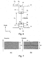
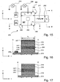
- the electronic band energy diagram includes valence and conduction band edges 34, 35.
- a first set of quasi-bound states 36 is formed in a first quantum well 37 defined by the valence band edge 34.
- a second set of quasi-bound states 38 is formed in a second quantum well 39 defined by the conduction band edge 35.
- bias V 1 between the source and drain terminals 7, 8 ( Figure 1) populates the first quantum well 37 with holes 40 1 , 40 2 with a hole density n A .
- the electron turnstile 6 ( Figure 1) introduces electrons 41 1 , 41 2 , 41 3 sequentially into second quantum well 39, beginning with the first electron 41 1 .
- a photon 30 is generated by the first electron 41 1 which is in a first state 42 1 combining with a hole 40 1 in a second state 43 1 .
- the photon generation region 2 ( Figure 1), charge-carrier controlling means 3 ( Figure 1) and optical control providing means 4 are arranged so as to cause the photon generation region 2 to emit photons at a given rate and of a given configuration.
- Configuration of a photon can be specified for example in terms of frequency, polarisation and direction of emission.
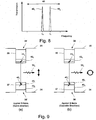
- a photonic band gap 45 is shown for a photonic crystal similar to the photonic crystal structure 13 ( Figure 1) except that it lacks the defect 15 ( Figure 1).
- the photonic crystal permits light to propagate if the light has a frequency above or below the photonic band gap 45.
- a photonic band gap 46 is shown for the photonic crystal structure 13 ( Figure 1).
- the defect 15 ( Figure 1) introduces a defect state 47. This allows light of a selected frequency ⁇ 0 to propagate through the photonic crystal structure 13 ( Figure 1) even if ⁇ 0 falls within the photon band gap 46.
- the photonic crystal structure 13 ( Figure 1) can be used to control whether photon 30 is emitted.
- first and second emission lines 48 1 , 48 2 are shown for the photon generation region 2.
- the emission lines 48 1 , 48 2 correspond to recombination of the first electron 40 1 in the first state 41 1 and a hole 41 1 , 41 2 in either the second state 42 1 or a third state 42 2 .
- the second and third states 42 1 , 42 2 may correspond to heavy and light hole states.
- the photonic band gap structure 13 may be used to select the first emission lines 48 1 . Thus, even though a sufficiently high bias may be applied between the source and drain terminals 7, 8 that photons of either frequency could be emitted, the photon band gap structure 13 can be employed so as to ensure that photons having the first frequency are generated ⁇ 0 .
- Selection rules for electronic transitions involving a photon and based on electric dipole interaction are used to configure the polarization of the emitted photon 30.
- the selection rules are based on quantum numbers comprising the principal quantum number n which governs the total energy of an electron (or hole), the orbital quantum number l which governs the magnitude of the an electron's angular momentum, the magnetic quantum number m l which governs the direction of the angular momentum and the spin quantum number m s .
- the orbital quantum number l is used to determine a magnitude of electron (or hole) angular momentum L .
- the magnetic quantum number m specifies a direction of vector L in the direction of an applied magnetic field B .
- the spin quantum number m s specifies the direction of a spin angular momentum S in the direction of an applied magnetic field B .
- Quantum numbers j and m j determine the magnitude and direction of J respectively.
- Applying a magnetic field in the photon generating region 2 can be used to shift energy states and resolve degenerate states.
- the magnetic field may be applied locally using second coil 17 2 or externally using a coil arrangement (not shown), such as a superconducting coil (not shown) provided in a cryostat (not shown).
- Applying magnetic fields in the channel 11 outside the photon generating region 2 can be used to select a spin polarization of charge carriers and thus, using the selection rules described earlier, help control polarisation of emitted photons.
- first and third coils 17 1 , 17 3 are used to help control spin polarisation.
- ferromagnetic contacts (not shown) or spin aligners may be used to select charge carriers of a given spin polarization. Thus, replacing a single contact with two contacts of different spin alignment allows charge carriers with different spin polarizations to be injected into the channel.
- the sixth and seventh voltage sources 23 1 , 23 2 drive currents through the first and third coils 17 1 , 17 3 in the same sense, for example in an anti-clockwise direction as viewed in Figure 1, and thus generate an upward magnetic fields (B ⁇ ) aligned parallel to the z-axis.
- An electron 41 1 from source 7 passes through the magnetic field generated by the first coil 17 1 and aligns its spin with the magnetic field.
- the electron 41 1 now with spin up ( ⁇ ), passes into the second quantum well 39.
- a hole 43 1 from drain 7 passes through the magnetic field created by the third coil 17 3 and aligns its spin with the magnetic field.
- the hole 43 1 also with spin up ( ⁇ ), passes into the second quantum well 39.
- the electron 41 1 and hole 43 1 recombine to generate a photon 30 1 which is plane-polarised.
- the orientation of the plane-polarised photon 30 1 may be varied by applying an electrical field E parallel to the z-axis by applying a bias to both arms of the second coil 17 2 relative to the source 7 or drain 8.
- the device 1 may be placed between parallel plates 338 1 , 338 2 ( Figure 26) across which a bias is applied.
- the orientation of the plane-polarised photon 30 1 may also be varied by applying an electrical field E perpendicular to the z-axis by applying a bias across side gates (not shown) disposed on sidewalls of vertical cavity structure 5.
- the orientation of the plane-polarised photon 30, may also be set by using an in-built electrical field generated in the layer structure, for example using modulation doping or by inducing strain.
- the sixth and seventh voltage sources 23 1 , 23 2 drive currents through the first and third coils 17 1 , 17 2 in the opposite senses, for example in an anti-clockwise and clockwise directions respectively as viewed in Figure 1, and thus generate magnetic fields aligned parallel and anti-parallel to the z-axis.
- An electron 41 1 from source 7 passes through the parallel magnetic field generated by the first coil 17 1 and aligns its spin with the magnetic field.
- the electron 41 1 with spin up ( ⁇ ), passes into the second quantum well 39.
- a hole 43 1 from drain 7 passes through the anti-parallel magnetic field created by the third coil 17 3 and aligns its spin with the anti-parallel magnetic field.
- the hole 43 1 , with spin down ( ⁇ ) passes into the second quantum well 39.
- the direction in which the photon 30 1 , 30 2 is emitted is selected by increasing the probability of emission in one direction.
- the photonic crystal structure 13 is arranged to be symmetrical, thereby favouring neither emission along the x-axis, nor the y-axis in any given direction.
- the vertical cavity structure 5 is arranged such that the transmisivity of the upper mirror layer 29 is greater than that of the lower mirror layer 25. This is achieved by using layers in the upper mirror layer 29 than in the lower mirror layer 25.
- the photon 30 1 , 30 2 is emitted through the upper mirror layer 29 and through the top surface of the vertical layer structure.
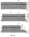
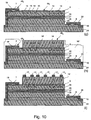
- a substrate 24' comprising semi-insulating GaAs is provided. Overlying layers 10', 25' 26', 27', 28', 29', 9' are sequentially grown using molecular beam epitaxy (MBE). Suitable MBE apparatus are well-known in the art.
- a p-type GaAs buffer layer (not shown) is grown on the substrate 24', doped in-situ with silicon (Si) to a concentration of 2x10 18 cm -3 .
- a first GaAs layer 10' is grown comprising n-type GaAs, doped in-situ with silicon (Si) to a concentration of 2 ⁇ 10 18 cm -3 and having a thickness of 200nm.
- a first mirror layer 25' is grown comprising 26.5 alternating layers of n-type AlAs and n-type Al 0.1 Ga 0.9 As, doped in-situ with Si to a concentration of 5 ⁇ 10 17 cm -3 and having layer thicknesses of each 711 ⁇ and 605 ⁇ respectively.
- a first AlGaAs layer 26' is grown comprising n-tppe Al 0.3 Ga 0.7 As doped in-situ with Si to a concentration of 5 ⁇ 10 17 cm -3 and having a thickness of 100 ⁇ .
- a second GaAs layer 27' is grown comprising intrinsic GaAs having a thickness of 60 ⁇ .
- a second AlGaAs layer 28' is grown comprising p-type Al 0.3 Ga 0.7 As, doped in-situ with carbon (C) to a concentration of 5 ⁇ 10 17 cm -3 and having a thickness of 100 ⁇ .
- a second mirror layer 25' is grown comprising 19 periods of alternating layers of p-type AlAs and p-type Al 0.1 Ga 0.9 As, doped with C to a concentration of 5 ⁇ 10 17 cm -3 and having layer thicknesses of each 711 ⁇ and 605 ⁇ respectively.
- a third GaAs layer 9' is grown comprising p-type GaAs, doped with C to a concentration of 2 ⁇ 10 18 cm -3 and having a thickness of 20nm.
- a first layer of photoresist (not shown) is applied over an first exposed surface 49 1 ( Figure 10a) of the third GaAs layer 9' and patterned using conventional photolithographic techniques so as to define a patterned photoresist mask (not shown).
- a wet etch in this example comprising a sulphuric acid/hydrogen peroxide/water (H 2 SO 4 /H 2 O 2 /H 2 O) mixture, is used to remove exposed portions of layers 9', 29', 28', 27', 26', 26', 10', 24', leaving etched layers 9", 29", 28", 27", 26", 26", 10", 24 and defining a mesa region 50.
- H 2 SO 4 /H 2 O 2 /H 2 O sulphuric acid/hydrogen peroxide/water
- Other wet etches may be used.
- a dry etch such as reactive ion etching using SiCl 4 as a feed gas, may be used.
- a second layer of photoresist (not shown) is applied over a second exposed surface 49 2 ( Figure 10b) and patterned using conventional photolithographic techniques so as to define a second patterned photoresist mask (not shown).
- Another H 2 SO 4 /H 2 O 2 /H 2 O wet etch is used to remove exposed portions of etched layers 9", 29", 28", 27", 26", 26", 10", 24, leaving layers 9"', 29"', 28, 27, 26, 26, 10, 24.
- Other wet etches, or a dry etch may be used.
- a first layer of electron-beam resist (not shown) is applied over a third exposed surface 49 3 ( Figure 10c) and patterned using conventional electron-beam lithographic techniques so as to define a first patterned electron-beam resist mask (not shown).
- a layer of Sn (not shown) which is 50 nm thick is evaporated and lifted-off so as to leave Sn metallisations 7', 8'.
- the metallisations 7', 8' are annealed using conventional rapid thermal annealing techniques.
- a second layer of electron-beam resist (not shown) is applied over a fourth exposed surface 49 4 ( Figure 10d) and patterned using conventional electron-beam lithographic techniques so as to define a second patterned electron-beam resist mask (not shown).
- a dry etch in this case a reactive ion etch using SiCl 4 as a feed gas, is used to etch holes 14 in portions of etched layers 9", 29" and leave layers 9, 29.
- a layer of polyimide 15' is applied over a fifth exposed surface 49 5 ( Figure 10e) and partially cured.
- the polyimide 15' substantially planarises features having lateral dimension of 1 ⁇ m or less.
- a layer of photoresist (not shown) is applied over the polyimide layer 15' and patterned using conventional photolithographic techniques so as to define a third patterned photoresist mask (not shown).
- a solvent is used to remove portions of polyamide layer15', leaving etched polyimide layer 15" in the mesa region 50 ( Figure 10c).
- the third patterned photoresist mask is removed.
- the etched polyimide 15" is fully cured and then globally etched-back using an oxygen (O 2 ) plasma until the top of the contact layer 9 is reached, thus leaving polyimide 15 within holes 14.
- O 2 oxygen
- a third layer of electron-beam resist (not shown) is applied over a sixth exposed surface 49 6 ( Figure 10f) and patterned using conventional electron-beam lithographic techniques so as to define a third patterned electron-beam resist mask (not shown).
- a Cr/Au layer (not shown) having Cr and Au thickness of 20 and 50 nm respectively layer is evaporated and lifted-off so as to leave source and drain leads 19, 20.
- This stage is also used to define gates 6 1 , 6 2 , 6 3 .
- the source and drain leads 19, 20 and gates 6 1 , 6 2 , 6 3 run out to large-area Au bondpads (not shown) to which wires (not shown) may be bonded.
- FIG. 10h another layer of polyimide 18' is applied over a seventh exposed surface 49 7 ( Figure 10g) and partially cured.
- a layer of photoresist (not shown) is applied over the polyimide layer 18' and patterned using conventional photolithographic techniques so as to define a fourth patterned photoresist mask (not shown).
- a solvent is used to remove portions of polyamide layer 18', leaving etched polyimide layer 18.
- the fourth patterned photoresist mask is removed and polyimide layer 18 is fully cured.
- a fourth layer of electron-beam resist (not shown) is applied over an eighth exposed surface 49 8 ( Figure 10h) and patterned using conventional electron-beam lithographic techniques so as to define a fourth patterned electron-beam resist mask (not shown).
- a Cr/Au layer (not shown) having Cr and Au thickness of 20 and 50 nm respectively layer is evaporated and lifted-off so as to leave coils 17 1 , 17 2 , 17 3 .
- the coils 17 1 , 17 2 , 17 3 run out to large-area Au bond pads (not shown) to which wires (not shown) may be bonded.
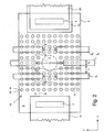
- the photon source 101 comprises a photon generation region 102, means 103 for controllably introducing a charge-carrier into the photon generation region 102 and means 104 for providing optical control over the photon generation region 102.
- the photon generation region 102 which in this example is a quantum dot formed in intrinsic gallium arsenide (GaAs), is embedded in a vertical cavity structure 105, which will be described in more detail later.
- GaAs intrinsic gallium arsenide
- the charge-carrier introducing means 103 includes a charge-carrier turnstile 106 disposed between source and drain terminals 107, 108.
- the source and drain terminals 107, 108 contact top and bottom contact layers 109, 110 respectively of the vertical cavity structure 105.
- a channel 111 is formed between source and drain terminals 107, 108.
- the charge-carrier turnstile 106 comprises a plurality of sets of gates 106 1 , 106 2 , 106 3 disposed on the vertical cavity structure 105.
- the set of gates 106 1 , 106 2 , 106 3 are offset from one another along the channel by a length s 1 preferably of the order of 0.1 or 1 ⁇ m.
- the gates within a pair of gates 106 1 , 106 2 , 106 3 are separated by a gap w 1 , w 2 , w 3 preferably of the order of 0.1 or 1 ⁇ m.
- gaps w 1 , w 3 for the first and second set of gates 106 1 , 106 3 are smaller than the gap w 2 for the second set of gates 106 2 .
- This arrangement helps to define the photon generation region 2 in the channel 11 between the second set of gates 106 2 .
- a single-electron turnstile is used 106 1 , 106 2 , 106 3 .
- the gates 106 1 , 106 2 , 106 3 deplete charge-carriers from regions of vertical cavity structure 105 lying beneath and adjacent to the gates. For example, if a sufficient large gate bias is applied to the first set of gates 106 1 , then a depletion region 112 ( Figure 12) extends between the first set of gates 106 1 and across the channel 111, so as to pinch-off the channel 111.
- the optical control providing means 104 includes a photonic crystal structure 113.
- a two-dimensional photonic crystal structure is used which comprises a lattice of cylindrical holes 114 etched into the surface of the vertical cavity structure 15.
- the holes 114 are filled with dielectric material 115.
- the holes 114 have a diameter ⁇ , preferably of the order of 10nm to 1 ⁇ m, for example 200nm.
- a square lattice is used, with a lattice constant a, preferably of the order of 10nm to 1 ⁇ m, for example 500nm.
- Other types of lattices may be used, such as rectangular, triangular or quasiperiodic lattices.
- a defect 116 in this example a region in which lattice sites lack holes 114, is disposed within the photonic crystal structure 113.
- the defect 116 is for creating optical defect states, which will be described in more detail later.
- An alternative photonic crystal structure may comprise a lattice of cylindrical pillars, which may be planarised with a dielectric.
- the optical control providing means 104 may optionally include magnetic field generating means 117 1 , 117 2 , 117 3 .
- the magnetic field generating means 117 1 , 117 2 , 117 3 comprises variable magnetic field generating means 117 1 , 117 2 , 117 3 in the form of coils.
- static magnetic field generating means for example in the form of a nano- or micro-magnet, may be also be used. Both static and variable magnetic field generating means may be used for example to provide a static magnetic field in one region of the device and a variable magnetic field in another part of the device.
- the magnetic field generating means 117 1 , 117 2 , 117 3 is disposed on a dielectric 118 which overlies the vertical cavity structure 105.
- magnetic field generating means 117 1 , 117 2 , 117 3 may be embedded within dielectric 118. Nano or micro-magnets may be placed directly on the vertical cavity structure 105.
- Source and drain leads 119, 120 are connected to the source and drain terminals 107, 108.
- First and second voltage sources 121 1 , 121 2 are used to apply a bias across the source 107 and drain 108 respectively.
- the first and second voltage sources 120 1 , 120 2 may be replaced by a single voltage source (not shown).
- Third, fourth and fifth voltage sources 122 1 , 122 2 , 122 3 are used to apply biases to the first, second and third sets of gates 106 1 , 106 2 , 106 3 respectively.
- the third, fourth and fifth voltage sources 122 1 , 122 2 , 122 3 are programmable sources or variable frequency sources which allow high-frequency signals, for example of the order or 1 to 100 MHz, to be applied.
- a single voltage source (not shown) and a phase-offset circuit may be used.
- Sixth, seventh and eighth voltage sources 123 1 , 123 2 , 123 3 are used to drive respective currents through coils 117 1 , 117 2 , 117 3 .
- the vertical cavity structure 105 is placed on a substrate 124 and comprises the bottom contact layer 110, an overlying lower mirror layer 125, an overlying lower cladding layer 126, an overlying active layer 127 which includes the photon generation region 102, an overlying upper cladding layer 128, an overlying upper mirror layer 129 and the top contact layer 109.
- the substrate 124 comprises semi-insulating gallium arsenide (GaAs).
- the bottom contact layer 110 comprises n-type GaAs, doped with silicon (Si) to a concentration of 2 ⁇ 10 18 cm -3 and having a thickness of 200nm.
- the active layer 127 comprises intrinsic GaAs having a thickness of 60 ⁇ .
- the top contact layer 109 comprises p-type GaAs, doped with C to a concentration of 2 ⁇ 10 18 cm -3 and having a thickness of 20nm.
- the etched holes 114 penetrate about 1 ⁇ m into the vertical cavity structure 5 as shown by the arrow d and are filled with dielectric 115, such as optical resist or polyimide.
- the dielectric is used to tune refractive index offset.
- the vertical cavity structure 105 is partially covered by an overlying dielectric layer 118 comprising polyimide and has a thickness of about 1 ⁇ m.
- the coils 117 1 , 117 2 , 117 3 are disposed on the dielectric layer 118 and comprises chromium/gold (Cr/Au) metallisation having thickness of 10 and 50 nm respectively.
- the source and drain terminals 107, 108 comprise alloyed tin (Sn) ohmic contacts, having a pre-alloying thickness of 50nm, and chromium/gold (Cr/Au) metallisation having thickness of 10 and 50 nm respectively.
- the gates 106 1 , 106 2 , 106 3 overlie unetched portions of the top contact layer 109 and dielectric 114 filling holes 113.
- the charge-carrier introducing means 103 and optical mode controlling means 4 are arranged so as to cause said photon generation region 102 to controllably emit photons 130 at a given rate and of a given configuration, as described earlier.
- the source 101 is arranged so as to emit light into a waveguide 131 ( Figure 13).
- the lower and upper mirror layers 125, 129 are arranged to be symmetric, thereby favouring neither vertical emission through upper or lower surfaces of the device 101.
- the vertical cavity structure 115 extends laterally so as to form a ridge waveguide 131 ( Figure 13).
- the defect 115 is arranged in the photonic crystal 113 such that there are fewer holes between the defect 115 and the waveguide 131, than there are in other directions, thus providing a channel favouring lateral emission of the photon 130 into the waveguide 131.
- the waveguide 131 widens and etched so as to have a cleaved vertical surface 132.
- a 'V'-groove 133 is arranged so as to allow an end of an optical fibre 134 to be placed within it and abut against the cleaved vertical surface 132. This arrangement allows photon 130 to pass down the waveguide 131, through the cleaved surface 132 and into the optical fibre 134.
- the laterally-emitting single photon source 101 described above may be modified so as to emit entangled pairs of photons. This is achieved by modifying the photonic crystal 113 so as to provide two channels in opposite directions and two corresponding waveguides 131 1 , 131 2 ( Figure 14).
- a modified photon source 101' is arranged so as to emit photons 130 1 , 130 2 in opposite directions, one photon 130 1 into a first waveguide 131 1 and the other photon 130 2 into a second waveguide 131 2 .
- Each waveguide 131 1 , 131 2 widens and etched so as to have a respective cleaved vertical surface 132 1 , 132 2 .
- Respective 'V'-groove 133 1 , 133 2 are arranged so as to allow an optical fibres 134 1 , 134 2 to be positioned and abut against respective cleaved vertical surfaces 132 1 , 132 2 .
- This arrangement allows the first photon 130 1 to pass down the first waveguide 131 1 , through the first cleaved surface 132 1 and into the first optical fibre 134 1 and the second photon 130 2 to pass down the second waveguide 131 2 , through the second cleaved surface 132 2 and into the second optical fibre 134 1 .
- the entangled pair of photons 130 1 , 130 2 is produced in substantially the same manner as described earlier. However, a higher bias is applied between the source and the drain terminals 107, 108, typically V S -V D ⁇ 2V 1 .
- the photon source 201 comprises a photon generation region 202, means 203 for controllably introducing a charge-carrier into the photon generation region 202 and means 204 for providing optical control over the photon generation region 202.
- the photon generation region 202 which in this example is a quantum dot formed in intrinsic gallium arsenide (GaAs), is embedded in a pillar structure 205 having etched sidewall 206.
- GaAs intrinsic gallium arsenide
- the charge-carrier introducing means 203 includes source and drain terminals 207, 208.
- First and second voltage sources 209, 210 are used to apply a bias across the terminals 207, 208 respectively.
- a photon 211 is emitted into a waveguide 212.
- the pillar structure 205 lies on a bottom contact layer 213 and comprises an overlying first low-doped layer 214, an overlying first barrier layer 215, an overlying well layer 216, an overlying second barrier layer 217, an overlying second low-doped layer 218 and an overlying top contact layer 219.
- the bottom contact layer 213 comprises an n-type GaAs substrate.
- the first low-doped layer 214 comprises n-type GaAs, doped with Si to a concentration of 1 ⁇ 10 16 cm -3 and having a thickness of 100nm.
- the first barrier layer 215 comprises undoped Al 0.3 Ga 0.7 As having a thickness of 4nm.
- the well layer 216 comprises p-type GaAs, doped with C to a concentration of 2 ⁇ 10 18 cm -3 and having a thickness of 7nm.
- the second barrier layer 217 comprises undoped Al 0.3 Ga 0.7 As having a thickness of 3nm.
- the second doped layer 218 comprises n-type GaAs, doped with Si to a concentration of 1 ⁇ 10 16 cm -3 and having a thickness of 100nm.
- the top contact layer 219 comprises n-type GaAs, doped with Si to a concentration of 2 ⁇ 10 18 cm -3 and having a thickness of 50nm.
- the first barrier layer 215 is arranged to be thicker than the second barrier layer 216.
- Barrier layers 215, 217 may have thicknesses as low as 2nm.
- first and second barrier layers 215, 217 may comprise n-type AlGaAs and may be thicker.
- the barrier layers 215, 217 may comprise n-type Al 0.3 Ga 0.7 As, doped with Si to a concentration of 2 ⁇ 10 18 cm -3 and may have a thickness of 10nm.
- the first and second low-doped layers 211, 213 may also be more heavily doped, for instance to a concentration of 1 ⁇ 10 17 cm -3 .
- first and second well layers may be used, each comprising p-type GaAs, doped with C to a concentration of 2 ⁇ 10 18 cm -3 and having a thickness of 9nm, having first and second barrier layers either side comprising undoped Al 0.3 Ga 0.7 As having a thickness of 4nm and separated by a third barrier layer comprising an undoped Al 0.3 Ga 0.7 As having a thickness of 3nm.
- first and second well layers may be used, each comprising p-type GaAs, doped with C to a concentration of 2x10 18 cm -3 and having a thickness of 5 nm, having first and second barrier layers either side comprise n-type Al 0.3 Ga 0.7 As, doped with Si to a concentration of 2 ⁇ 10 18 cm -3 and may have a thickness of 10nm, and separated by a third barrier layer comprising an undoped Al 0.3 Ga 0.7 As having a thickness of 3nm.
- the source terminal 207 and first and second drain terminals 208 1 , 208 2 contact the top and bottom contact layers 213, 219 respectively and comprise cobalt (Co) metallisation having thickness of 50 nm respectively.
- Co cobalt
- Other ferromagnetic materials, such as Dysprosium (Dy) or Nickel (Ni) may be used.
- Gold overlying layers may be provided.
- the source and train terminals 207, 208 1 , 208 2 provide spin aligners for injecting charge carriers into the top and bottom contact layers 213, 219 of a specified spin.
- the spin is specified by polarising the terminals 207, 208 1 , 208 2 before the photon source 201 is used.
- a first insulating layer 220 overlies the pillar structure 205 and exposed bottom contact layer 213 having windows 221 1 , 221 2 for allowing metallisations 222 1 , 222 2 to contact the drain terminals 208 1 , 208 2 .
- a metallisation 223 is provided to contact the source terminal 207.
- a second insulating layer 224 overlies the first insulating layer 220 on which are disposed first, second and third coils 225 1 , 225 2 , 225 3 arranged over respective terminals 207, 208 1 , 208 2 .
- the first, second and third coils 225 1 , 225 2 , 225 3 provide magnetic fields for polarising the terminals 207, 208 1 , 208 2 .
- the insulating layers 220, 224 preferably comprise polyimide.
- the coils 225 1 , 225 2 , 225 3 preferably comprise a layer of chromium with an overlying layer of gold.
- the optical control providing means 204 is provided by etched sidewalls 206.
- the pillar structure 205 is rectangular in plan view with sides having dimensions b 1 , b 2 .
- the pillar structure 205 may be circular in plan view.
- the pillar structure 205 may have a side or diameter b ⁇ 50nm.
- the optical control providing means 4 may include further magnetic field generating means (not shown).
- the magnetic field generating means may comprise variable magnetic field generating means in the form of a coil (not shown), looped around the foot of the pillar structure 205.
- a dielectric such as silicon dioxide or silicon nitride is used to insulate the coil (not shown) from bottom contact layer 211.
- Coulomb blockade is employed to controllably introduce a charge-carrier into the photon generation region 202.
- the source 201 is arranged to exhibit a Coulomb staircase in I-V characteristic (not shown).
- Any applied bias applied between the source and drain terminals 207, 208 falls across the first doped region 214, the barrier and well layers 215, 216, 217 and the second doped region 218.
- a proportion ⁇ of the applied bias fall across the barrier and well layers 215, 216, 217.
- the bias which falls across the barrier and well layers 215, 216, 217 is just larger than the Coulomb gap, i.e. ⁇ V 1 > e/2C, thus resulting in current I, corresponding to one electron at a time.
- the waveguide 212 is coupled to an optical fibre (not shown) in a manner hereinbefore described.
- the waveguide 212 may be provided with one or more sets of gates 226.
- a set of gates 226 comprises a pair of gates 226 1 , 226 2 disposed on respective sidewalls 227 of the waveguide 212.
- An insulating layer 228 is provided to electrically insulate the gates 226 1 , 226 2 from the waveguide 212 and the bottom contact layer 213.
- a voltage source 229 applies a bias between the gates 226 1 , 226 2 so as to provide a lateral electric field E rot , in this example along the y-axis, for rotating the plane on polarization of the photon 211.
- a set of gates 226 may comprise a single gate overlying the waveguide 212 for applying a vertical electric field E rot , i.e. in the direction of the z-axis.
- the photon source 201 just described uses intrinsic antibunching of electrons to provide antibunched photons.
- a single-electron turnstile can be used, for example comprising surface gated or side-gated arrangements.
- a method of fabricating the source 201 includes defining the source terminal 207 by patterning a layer of positive electron-beam resist (not shown), evaporating a layer of Co, and optionally an overlying layer of Au, and lifting-off unwanted metallisation.
- the method also includes patterning a layer of negative electron-beam resist (not shown) for the waveguide 212.
- the method includes defining the pillar structure 205 and waveguide 212 by using an anisotropic, reactive ion etch (RIE) using silicon tetrachloride (SiCl 4 ) and Argon (Ar) as feed gases.
- RIE reactive ion etch
- SiCl 4 silicon tetrachloride
- Ar Argon
- the method then includes defining the drain terminal 208 by patterning another layer of positive electron-beam resist (not shown), evaporating a layer of Co, and optionally an overlying layer of Au, and lifting-off unwanted metallisation.
- the Co metallisation may be annealed using a rapid thermal anneal (RTA) process.
- RTA rapid thermal anneal
- the pillar structure is planarised using a layer of polyimide 220. Windows 221 1 , 221 2 are opened in the layer of polyimide 220 to contact the drain terminals 208 1 , 208 2 and then is globally etched back using an O 2 plasma etch to reveal the top of the pillar structure 205.
- Metal contacts 222 1 , 222 2 , 223 are defined by patterning a layer of optical resist and evaporating a layer of Cr and a layer of Au, and lifting-off unwanted metallisation.
- the structure is planarised by another layer of polyimide 224.
- Coils 225 1 , 225 2 , 225 3 are defined by patterning a layer of optical resist and evaporating a layer of Cr and a layer of Au, and lifting-off unwanted metallisation.
- the photon sources 1, 101, 201 hereinbefore described may also operate as photon detectors.
- a constant voltage V 4 is applied by the first and second voltage source 21 1 , 21 2 .
- the bias voltage V 4 is sufficiently small that photon emission does not occur.
- an incoming photon (not shown) can create an electron-hole pair which are swept to respective contact region 7, 8 resulting in an increased current.
- the photon sources 1, 101, 201 may be provided with spin aligned contacts by using for example Co instead of AuGeNi in the source and drain contacts 7, 8 and providing coils (not shown) or permanent magnets (not shown) to align the contacts with a given polarization.
- the current generated by an electron-hole pair depends on alignment of the carrier spin with the contact.
- a photon detector is described in EP-A-1077492.
- the photon sources 1, 101, 201 hereinbefore described may used as a quantum computer.
- basis states may be defined as:
- a qubit When the system is sufficiently cooled, for example to 20mK using a dilution refrigerator (not shown), a qubit may be prepared as a superposition of quantum states. If the quantum states remain coherent for long enough, then the qubit may be manipulated.
- a bias V 3 is applied across the first coil 17 1 so as to drive a current anti-clockwise through the coil (as seen from above the device) and so generate an upward magnetic field B ⁇ .
- An electron is placed on the quantum dot 2. This is achieved using the train of gate voltage pulses described earlier.
- the electron on the quantum dot 2 is in a spin up state ⁇ (aligned with B ⁇ ) since this state has an energy E ⁇ which is lower than an energy E ⁇ the spin down state ⁇ (anti-parallel to B ⁇ ).
- a bias V 3 is applied across the third coil 17 3 so as to drive a current anti-clockwise through the coil (as seen from above the device) and so generate an upward magnetic field B ⁇ .
- a hole is placed on the quantum dot 2. This is achieved using the train of gate voltage pulses described earlier.
- the hole on the quantum dot 2 is in a spin up state ⁇ (aligned with B ⁇ ) since this state has an energy E ⁇ which is lower than an energy E ⁇ the spin down state ⁇ (anti-parallel to B ⁇ ).
- the photonic crystal structure 13 is used to suppress photon emission. This is achieved by applying a uniform electric field E so as to alter the refractive index of, inter alia , active channel 27 which is formed of piezoelectric GaAs. In this case E o is of the order of 10 6 Vcm -1 .
- the uniform electric field E is applied by placing the device between parallel plate electrodes 338 1 , 338 2 ( Figure 26).
- a surface gate (not shown) with a corresponding dielectric (not shown) for isolating the surface gate from the coil 17 and underlying layers may be provided. Accordingly, gate biases V G1 , V G2 , V G3 applied to the gates 6 1 , 6 2 , 6 3 may be adjusted to compensate.
- the biases applied to the first and third coils 17 1 , 17 3 may be removed to remove magnetic fields B ⁇ . Thus, the system is left in state
- ⁇ i ⁇ is performed.
- the transformation is a unitary transformation U t and is performed as follows:
- the time-varying electric field E h ⁇ is applied using the parallel plate electrodes (not shown).
- the system undergoes Rabi oscillations between the spin up state ⁇ and the spin down state ⁇ .
- the time-varying electric field E h ⁇ is applied for a period of time t. This transforms the initial state
- the uniform electric field E is removed, thereby allowing a photon to be emitted.
- a detector for example another photon source operating as a photon detector, the polarization of the photon is measured.
- the process is repeated N times and the number of times
- By varying the pre-determined time t it is possible to determine a time t H needed to effect the so-called Hadamard Transformation U H .
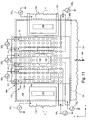
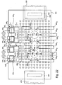
- FIG. 21 an embodiment of a single-qubit quantum computer 300 according to the present invention is shown which comprises a pair of photon sources 301 A , 301 B .
- the quantum computer 300 comprises first and second photon generation regions 302 A , 302 B , first and second means 303 A , 303 B for controllably introducing a charge-carrier into respective photon generation regions 302 A , 302 B and means respective means 304 A , 304 B for providing optical control within the photon generation region 302 A , 302 B .
- the first and second photon generation regions 302 A , 302 B which in this example each comprise a respective quantum dot formed in intrinsic GaAs, is embedded in a vertical cavity structure 305, which will be described in more detail later.
- the charge-carrier introducing means 303 A , 303 B includes a charge-carrier turnstiles 306 A , 306 B disposed between source and drain terminals 307, 308.
- the source and drain terminals 307, 308 contact top and bottom contact layers 309, 310 respectively of the vertical cavity structure 305.
- a channel 311 is formed between source and drain terminals 307, 308.
- the charge-carrier turnstiles 306 A , 306 B comprise a plurality of sets of gates 306 A1 , 306 C1 , 306 A2 , 306 C2 , 306 A3 , 306 C3 , 306 B1 , 306 C4 , 306 B2 , 306 C5 , 306 B3 , 306 C6 disposed on the vertical cavity structure 5.
- the first turnstile 306 A comprises first, second and third sets of gates 306 A1 , 306 C1 , 306 A2 , 306 C2 , 306 A3 , 306 C3 , each set comprising an independent surface gate 306 A1 , 306 A2 , 306 A3 and a corresponding finger 306 C1 , 306 C2 , 306 C3 of a common, multi-fingered surface gate 306 C and arranged in a split-gate configuration.
- the second turnstile 306 B comprises first, second and third sets of gates 306 B1 , 306 C4 , 306 B2 , 306 C5 , 306 B3 , 306 C6 , each set comprising an independent surface gate 306 B1 , 306 B2 , 306 B3 and a corresponding finger 306 C4 , 306 C5 , 306 C6 of the common, multi-fingered surface gate 306 C and arranged in a split-gate configuration.
- the set of gates 306 A1 , 306 C1 , 306 A2 , 306 C2 , 306 A3 , 306 C3 , 306 B1 , 306 C4 , 306 B2 , 306 C5 , 306 B3 , 306 C6 are offset from one another along the channel by a length s 1 preferably of the order of 0.1 or 1 ⁇ m.
- Each gate 306 A1 , 306 A2 , 306 A3 , 306 B1 , 306 B2 , 306 B3 is separated from a corresponding finger of the common surface gate 306 C by a gap of the order of 0.1 or 1 ⁇ m.
- 306 C4 of the common surface gate 306 C are smaller than the gaps w 2 , w 4 between the second and fifth gates 306 A2 , 306 B2 and corresponding fingers 306 C2 , 306 C5 of the common surface gate 306 C .
- This arrangement helps to define the photon generation regions 302 A , 302 B in the channel 311 between the second and fifth gates 306 A2 , 306 B2 and corresponding fingers 306 C2 , 306 C5 .
- the gates 306 A1 , 306 A2 , 306 A3 , 306 B1 , 306 B2 , 306 B3 , 306 C deplete charge-carriers from regions of vertical cavity structure 305 lying beneath and adjacent to the gates. For example, if a sufficient large gate bias is applied to the first gate 306 A1 , then a depletion region 312 extends between the first gates 306 A1 and the corresponding finger 306 C1 of the common date 306 C , and across the channel 311, so as to pinch-off the channel 311.
- the optical control providing means 304 A , 304 B includes a photonic crystal structure 313.
- a two-dimensional photonic crystal structure is used which comprises a lattice of holes 314, preferably cylindrical, etched into the surface of the vertical cavity structure 305.
- the holes 314 are filled with dielectric material 315.
- the holes 314 have a diameter ⁇ preferably of the order of 10nm to 1 ⁇ m.
- ⁇ may be 200nm.
- a square lattice is used, with a lattice constant a preferably of the order of 10nm to 1 ⁇ m.
- lattice constant a may be 500nm.
- Other types of lattices may be used, such as rectangular, triangular or quasiperiodic lattices.
- First and second defects 316 A , 316 B are disposed within the photonic crystal structure 313 and connected by a channel 316'. The first and second defects 316 A , 316 B are in the form of respective regions in which lattice sites lack holes 314.
- the defects 316 A , 316 B are for creating optical defect states.
- the channel 316' is in the form of a region which lattice sites lack holes which increase transmissivity.
- An alternative photonic crystal structure may comprise a lattice of cylindrical pillars, which may be planarised with a dielectric.
- the optical control providing means 304 A , 304 B may optionally include magnetic field generating means 317 1 , 317 2 , 317 3 , 317 4 , 317 5 .
- each magnetic field generating means 317 1 , 317 2 , 317 3 , 317 4 , 317 5 each comprises a variable magnetic field generating means 317 1 , 317 2 , 317 3 , 317 4 , 317 5 in the form of a coil.
- static magnetic field generating means for example in the form of a nano- or micro-magnet, may be also be used.
- the magnetic field generating means 317 1 , 317 2 , 317 3 , 317 4 , 317 5 are disposed on a dielectric 318 which overlies the vertical cavity structure 305.
- Source and drain leads 319, 320 are connected to the source and drain terminals 307, 308.
- First and second voltage sources 321 1 , 321 2 are used to apply a bias across the source 307 and drain 308 respectively.
- the first and second voltage sources 320 1 , 320 2 may be replaced by a single voltage source (not shown).
- Third, fourth and fifth voltage sources 322 A1 , 322 A2 , 322 A3 are used to apply biases to the first, second and third gates 306 A1 , 306 A2 , 306 A3 respectively.
- sixth, seventh and eighth voltage sources 322 B1 , 322 B2 , 322 B3 are used to apply biases to the first, second and third sets of gates 306 B1 , 306 B2 , 306 B3 respectively.
- the third, fourth, fifth sixth, seventh and eighth voltage sources 322 A1 , 322 A2 , 322 A3 , 322 B1 , 322 B2 , 322 B3 are programmable sources or variable frequency sources which allow high-frequency signals, preferably of the order or 1 to 100 MHz, to be applied.
- a single voltage source (not shown) and a phase-offset circuit (not shown) may be used.
- Ninth, tenth, eleventh, twelfth and thirteenth voltage sources 323 A , 323 B , 323 C , 323 D , 323 E are used to drive a current through the first, second, third, fourth and fifth coils 317 1 , 317 2, 317 3 , 317 4 , 317 5 respectively.
- first and second means 324 1 , 324 2 for detecting charge are provided in the form of single-electron transistors.
- the first single-electron transistor 324 1 comprise a channel 325 1 disposed between source and drain regions 326 1 , 327 1 .
- the channel 325 1 is formed in the bottom contact later 310 and is configured as a so-called "nanowire" for exhibiting Coulomb blockade.
- the source and drain regions 326 1 , 327 1 contact the bottom contact layer 309.
- the nanowire 325 1 and source and drain region 326 1 , 327 1 are electrically isolated from the cavity structure 305 by trench isolation 328 1 .
- the transistor 324 1 is provided with a voltage source 329 1 and current detector 330 1 . The presence or absence of excess charge in the first quantum dot 302 A is detected by measuring changes in current through channel 325 1 .
- the second single-electron transistor 324 2 comprise a channel 325 2 disposed between source and drain regions 326 2 , 327 2 .
- the channel 325 2 is formed in the bottom contact later 310 and is configured as a nanowire for exhibiting Coulomb blockade.
- the source and drain regions 326 2 , 327 2 contact the bottom contact layer 309.
- the nanowire 325 2 and source and drain region 326 2 , 327 2 are electrically isolated from the cavity structure 305 by a trench isolation 328 2 .
- the transistor 324 2 is provided with a voltage source 329 2 and current detector 330 3 .
- the presence or absence of excess charge in the second quantum dot 302 B is detected by measuring changes in current through channel 325 2 .
- charge detecting means may be used.
- metal-based single-electron transistors may be used similar to that described in "Observation of single-electron charging effects in small tunnel junctions" T. A. Fulton and G. J. Dolan, Physical Review Letters, volume 59, p 109 (1987).
- the charge detecting means may be arranged closer to, in plane with, over or under the quantum dots 302 A , 302 B .
- the vertical cavity structure 305 is placed on a substrate 331 and comprises the bottom contact layer 310, an overlying lower mirror layer 332, an overlying lower cladding layer 333, an overlying active layer 334 which includes the photon generation regions 302 A , 302 B , an overlying upper cladding layer 335, an overlying upper mirror layer 336 and the top contact layer 309.
- the substrate 331 comprises semi-insulating gallium arsenide (GaAs).
- the bottom contact layer 310 comprises n-type GaAs, doped with Si to a concentration of 2 ⁇ 10 18 cm -3 and having a thickness of 200nm.
- the lower mirror layer 332 comprises 26.5 alternating layers of n-type AlAs and n-type Al 0.1 Ga 0.9 As, doped with Si to a concentration of 5 ⁇ 10 17 cm -3 and having layer thicknesses of each 711 ⁇ and 605 ⁇ respectively.
- the lower cladding layer 333 comprises n-type Al 0.3 Ga 0.7 As, doped with Si to a concentration of 5 ⁇ 10 17 cm -3 and having a thickness of 100 ⁇ .
- the active layer 334 comprises intrinsic GaAs having a thickness of 60 ⁇ .
- the upper cladding layer 335 comprises p-type Al 0.3 Ga 0.7 As, doped with C to a concentration of 5 ⁇ 10 17 cm -3 and having a thickness of 100 ⁇ .
- the upper mirror layer 336 comprises 19 periods of alternating layers of p-type AlAs and p-type Al 0.1 Ga 0.9 As, doped with C to a concentration of 5 ⁇ 10 17 cm -3 and having layer thicknesses of each 711 ⁇ and 605 ⁇ respectively.
- the top contact layer 309 comprises p-type GaAs, doped with C to a concentration of 2 ⁇ 10 -3 cm -3 and having a thickness of 20nm.
- the etched holes 314 penetrate about 1 ⁇ m into the vertical cavity structure 305 as shown by the arrow d and are filled with dielectric 315, such as optical resist or polyimide.
- the dielectric is used to tune refractive index offset.
- the vertical cavity structure 305 is partially covered by an overlying dielectric layer 318 comprising polyimide and has a thickness of about 1 ⁇ m.
- the coils 317 1 , 317 2 , 317 3 , 317 4 , 317 5 are disposed on the dielectric layer 318 and comprises chromium/gold (Cr/Au) metallisation having thickness of 10 and 50 nm respectively.
- the source and drain terminals 307, 308 comprise alloyed tin (Sn) ohmic contacts, having a pre-alloying thickness of 50nm, and chromium/gold (Cr/Au) metallisation having thickness of 10 and 50 nm respectively.
- the gates 306 A1 , 306 A2 , 306 A3 overlie unetched portions of the top contact layer 309 and dielectric 315 filling holes 314.
- the first and second quantum dots 302 A , 302 B may be coupled through an electrostatic interaction, through the exchange of a virtual photon and/or through the exchange of a real photon. Electrostatic coupling tends to dominate when the first and second quantum dots 302 A , 302 B are separated by a relatively small distance, for example by a distance of the order of 1 to 100nm. Photon exchange coupling tends to dominate when the first and second quantum dots 302 A , 302 B are separated by a relatively large distance, for example by distances of the order of 1 ⁇ m or greater.
- the first and second quantum dots 302 A , 302 B provides a two-state system based on electron charge similar to that described in EP-A-1262911.
- Basis states may be defined as follows:
- a qubit When the system is sufficiently cooled, for example to 20mK using a dilution refrigerator (not shown), a qubit may be prepared as a superposition of quantum states. If the quantum states remain coherent for long enough, then the qubit may be manipulated.
- An electron is placed on the first quantum dot 302 A .
- This is achieved using the train of gate voltage pulses in a manner similar to that described earlier.
- the photonic crystal structure 313 is used to suppress photon emission. This is achieved by applying a uniform electric field E so as to alter the refractive index of active channel 327. Application of the electric field changes the refractive index of the active channel 327 because the channel 327 is formed from GaAs, which is piezoelectric. In this case E o is of the order of 10 6 Vcm -1 .
- the uniform electric field E is applied by placing the device 301 carried on chip 337 between parallel plate electrodes 338 1 , 338 2 .
- a voltage source 339 applies a potential V between the electrodes 338 1 , 338 2 .
- a surface gate (not shown) with a corresponding dielectric (not shown) for isolating the surface gate from the coils 317 1 , 317 2 , 317 3 , 317 4 , 317 5 and underlying layers may be provided.
- gate biases V G11 , V G12 , V G13 , V G21 , V G22 , V G23 applied to the gates 306 A1 , 306 A2 , 306 A3 , 306 B1 , 306 B2 , 306 B3 may be adjusted to compensate.
- the system is left in state
- ⁇ i ⁇ is performed.
- the transformation is a unitary transformation U t and is performed as follows:
- the uniform electric field E is removed for a predetermined amount of time t. This permits emission of a photon 330 by the first quantum dot 302 A .
- the configuration of the channel 316' permits an electron to be emitted towards the second quantum dot 302 B .
- the photon can be absorbed the second quantum dot 302 B , then re-emitted towards the first quantum dot 302 A . This process may be repeated. Transmission of the photon is suppressed by reapplying the uniform electric field E.
- the exchange of a real photon (or a virtual photon) results in a final state
- ⁇ i ⁇ may be performed using an electrostatic interaction. This is achieved by removing or reducing bias V G31 , V G12 applied to the third and fourth gates 306 A3 , 306 B1 , thereby permitting charge tunnelling between the first and second quantum dots 302 A , 302 B .
- the process is repeated N times and the number of times
- By varying the pre-determined time t it is possible to determine a time t H needed to effect the so-called Hadamard Transformation U H .
- the first and second quantum dots 302 A , 302 B may be configured as two qubit quantum computer, each quantum dots 302 A , 302 B providing two-state system.
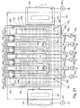
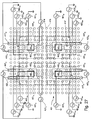
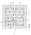
- the multiple photon source/multiple-qubit quantum computer 400 is shown in plan view without leads for contacting terminals and gates for the sake of clarity.
- the multiple photon source/multiple-qubit quantum computer 400 comprises an array of photon sources 401 11 , 401 22 , 401 12 , 401 22 .
- the photon sources 401 11 , 401 22 , 401 12 , 401 22 comprises first, second, third and fourth photon generation regions 402 11 , 402 22 , 402 12 , 402 22 , first, second, third and fourth means 403 11 , 403 22 , 403 12 , 403 22 for controllably introducing a charge-carrier into respective photon generation regions 402 11 , 402 22 , 402 12 , 402 22 and respective means 404 11 , 404 22 , 404 12 , 404 22 for providing optical control over the photon generation region 402 11 , 402 22 , 402 12 , 402 22 .
- the first, second, third and fourth photon generation regions 402 11 , 402 22 , 402 12 , 402 22 each comprise a respective quantum dot formed in intrinsic gallium arsenide (GaAs), embedded in a vertical cavity structure 405.
- GaAs intrinsic gallium arsenide
- the charge-carrier introducing means 403 11 , 403 22 , 403 12 , 403 22 includes means for providing electrostatic confinement 406 11 , 406 22 , 406 12 , 406 22 .
- Each photon source 401 11 , 401 22 , 401 12 , 401 22 is provided with a respective source terminals 407 11 , 407 12 , 407 21 , 407 22 .
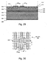
- a common drain terminal 408 ( Figure 29) is also provided.
- the source terminals 407 11 , 407 12 , 407 21 , 407 22 contact a top contact layer 409 of the vertical cavity structure 305 and the drain terminal 408 ( Figure 28) contacts a bottom contact layer 410.
- vertical channels 411 11 , 411 12 , 411 21 , 411 22 are formed between respective source terminals 407 1 , 407 2 , 407 3 , 407 4 and the drain terminal 408.
- the source terminals 407 1 , 407 2 , 407 3 , 407 4 provide spin aligners for injecting charge carriers into the top contact layers 409 with a specified spin.
- the drain terminal 408 ( Figure 28) provides a spin aligner for injecting charge carriers into the bottom contact layer 410.
- the means for providing electrostatic confinement 406 11 , 406 22 , 406 12 , 406 22 comprise a plurality of sets of gates 406 11A , 406 11B , 406 11C , 406 21A , 406 21B , 406 21C , 406 12A , 406 12B , 406 12C , 406 22A , 406 22B , 406 22C disposed on the vertical cavity structure 405.
- the first means for providing electrostatic confinement 406 11 includes first, second and third sets of gates 406 11A , 406 11B , 406 11C , each set of gates 406 11A , 406 11B , 406 11C comprising a pair of surface gates arranged in a split-gate configuration.
- the second means for providing electrostatic confinement 406 11 includes first, second and third sets of gates 406 12A , 406 12B , 406 13C , each set of gates 406 12A , 406 12B , 406 12C et cetera.
- the set of gates 406 11A , 406 11B , 406 11C are offset from one another by a length s, preferably of the order of 10nm to 1 ⁇ m.
- the gates within a pair of gates 406 11A , 406 11B , 406 11C are separated by a gap of the order of 10nm to 1 ⁇ m.
- gaps w 1 , w 3 for the first and third set of gates 406 11A , 406 11C are smaller than the gap w 2 for the second set of gates 406 11B . This arrangement helps to define the photon generation regions 402 11
- the gates 406 11A , 406 11B , 406 11C , 406 21A , 406 21B , 406 21C , 406 12A , 406 12B , 406 12C , 406 22A , 406 22B , 406 22C deplete charge-carriers from regions of vertical cavity structure 405 lying beneath and adjacent to the gates. For example, a depletion region 412 is shown under the second set of gates 406 22B of the fourth photon sources 401 22 .
- the optical control providing means 404 11 , 404 12 , 404 21 , 404 22 includes a photonic crystal structure 413.
- a two-dimensional photonic crystal structure is used which comprises a lattice of holes 414, preferably cylindrical, etched into the surface of the vertical cavity structure 405.
- the holes 414 are filled with dielectric material 415.
- the holes 414 have a diameter ⁇ preferably of the order of 0.1 or 1 ⁇ m.
- diameter ⁇ may be 200nm.
- a square lattice is used, with a lattice constant a preferably of the order of 0.1 or 1 ⁇ m.
- lattice constant a may be 500nm.
- Other types of lattices may be used, such as rectangular, triangular or quasiperiodic lattices.
- First, second, third and fourth defects 416 11 , 416 12 , 416 21 , 416 22 are disposed within the photonic crystal structure 413 and connected by channels 416 1 ', 416 2 '.
- the defects 416 11 , 416 12 , 416 21 , 416 22 are in the form of respective regions in which lattice sites lack holes 414.
- the defects 416 11 , 416 12 , 416 21 , 416 22 are for creating optical defect states.
- the channels 416 1 ', 416 2 ' are in the form of a region which lattice sites lack holes which increase transmissivity.
- An alternative photonic crystal structure may comprise a lattice of cylindrical pillars, which may be planarised with a dielectric.
- the optical control providing means 404 11 , 404 12 , 404 21 , 404 22 is further modified to promote or suppress particular types of polarization and/or particular planes of polarization.
- a hole 414' is omitted.
- other modifications may be made such as altering the vertical cavity, the shape of optical defect state, or providing material with in-built electric fields.
- the optical mode controlling means 304 A , 304 B includes magnetic field generating means 417 11 , 417 12 , 417 21 , 417 22 for polarising spin contacts 407 1 , 407 2 , 407 3 , 407 4 .
- magnetic field generating means 417 11 , 417 12 , 417 21 , 417 22 are in the form of coils. However, nano- or micro-magnets may be provided.
- the coils 417 11 , 417 12 , 417 21 , 417 22 are arranged to provide vertical magnetic fields, i.e. parallel or anti-parallel to the z-axis.
- the first and second coils 417 11 , 417 12 are each provided with an additional arm 417 11 ', 417 12 ' for providing a lateral magnetic field.
- the lateral magnetic field is used to configure circularly polarised photons of a given orientation.
- First, second, third and fourth voltage sources 421 11 , 421 12 , 421 21 , 421 22 are used to apply a bias across respective sources terminals 407 11 , 407 12 , 407 21 , 407 22 and the drain terminal 408.
- Fifth to thirteenth voltage sources 422 11A , 422 11B , 422 11C , 422 12A , 422 12B , 422 12C , 422 21A , 422 21B , 422 21C , 422 22A , 422 22B , 422 22C are used to apply biases to gates 406 11A , 406 11B , 406 11C , 406 21A , 406 21B , 406 21C , 406 12A , 406 12B , 406 12C , 406 22A , 406 22B , 406 22C respectively.
- Fourteenth to eighteenth voltage sources 423 11 , 423 12 , 423 21 , 423 22 are used to apply biases to coils 417 11 , 417 12 , 417 21 , 417 22 respectively.
- Nineteenth and twentieth voltage sources 423 11 ', 423 12 ' are used to apply biases to between respective first arms and additional arms of coils 417 11 , 417 12 .
- the vertical cavity structure 405 is placed on a substrate 424 and comprises the bottom contact layer 410, an overlying lower mirror layer 425, an overlying lower cladding layer 426, an overlying active layer 427 which includes the photon generation regions 402 11 , 402 12 , 402 21 , 402 22 , an overlying upper cladding layer 428, an overlying upper mirror layer 429 and the top contact layer 409.
- the substrate 424 comprises semi-insulating gallium arsenide (GaAs).
- the bottom contact layer 410 comprises n-type GaAs, doped with Si to a concentration of 2 ⁇ 10 18 cm -3 and having a thickness of 200nm.
- the lower mirror layer 425 comprises 26.5 alternating layers of n-type AlAs and n-type Al 0.1 Ga 0.9 As, doped with Si to a concentration of 5 ⁇ 10 17 cm -3 and having layer thicknesses of each 711 ⁇ and 605 ⁇ respectively.
- the lower cladding layer 426 comprises n-type Al 0.3 Ga 0.7 As, doped with Si to a concentration of 5 ⁇ 10 17 cm -3 and having a thickness of 100 ⁇ .
- the active layer 427 comprises intrinsic GaAs having a thickness of 60 ⁇ .
- the upper cladding layer 428 comprises p-type Al 0.3 Ga 0.7 As, doped with C to a concentration of 5x10 17 cm -3 and having a thickness of 100 ⁇ .
- the upper mirror layer 425 comprises 19 periods of alternating layers of p-type AlAs and p-type Al 0.1 Ga 0.9 As, doped with C to a concentration of 5 ⁇ 10 17 cm -3 and having layer thicknesses of each 711 ⁇ and 605 ⁇ respectively.
- the top contact layer 409 comprises p-type GaAs, doped with C to a concentration of 2 ⁇ 10 18 cm -3 and having a thickness of 20nm.
- the etched holes 414 penetrate about 1 ⁇ m into the vertical cavity structure 405 as shown by the arrow d and are filled with dielectric 415, such as optical resist or polyimide.
- the dielectric is used to tune refractive index offset.
- the source and drain terminals 407 11 , 407 12 , 407 21 , 407 22 , 408 comprise cobalt (Co) having a thickness of 50nm.
- the source and drain terminals 407 11 , 407 12 , 407 21 , 407 22 , 408 may also be provided with a gold overlayer having thickness of 50 nm.
- the gates 406 11A , 406 11B , 406 11C , 406 21A , 406 21B , 406 21C , 406 12A , 406 12B , 406 12C , 406 22A , 406 22B , 406 22C overlie unetched portions of the top contact layer 309 and dielectric 415 filling holes 414.
- the multiple photon source/multiple-qubit quantum computer 400 is covered by successive layers of dielectric 450, 451, 452.
- Vertical connection portions 453, 454 are used to connect gates, such as 406 22B , and source terminals, such as terminal 407 22 , and the gates 406 22B , to leads 455, 456.
- the quantum dots 402 11 , 402 22 , 402 12 , 402 22 may be coupled through an electrostatic interaction, through the exchange of a virtual photon and/or through the exchange of a real photon. Electrostatic coupling tends to dominate when quantum dots 402 11 , 402 22, 402 12, 402 22 are separated by a relatively small distance, for example by a distance of the order of 1 to 100nm. Photon exchange coupling tends to dominate when quantum dots 402 11 , 402 22 , 402 12 , 402 22 are separated by a relatively large distance, for example by distances of the order of 1 ⁇ m or greater.
- Input channels 457 11 , 457 12 , 457 21 , 457 22 can be used to supply photons to corresponding quantum dots 402 11 , 402 22 , 402 12 , 402 22 .
- Output channels 458 11 , 458 12 , 458 21 , 458 22 can be used to collect photons from corresponding quantum dots 402 11 , 402 22 , 402 12 , 402 22 .
- the quantum dots 402 11 , 402 22 , 402 12 , 402 22 interact through nearest neighbour channels 459 1 , 459 2 , 459 3 , 459 4 .
- quantum dots 402 11 , 402 22 , 402 12 , 402 22 also interact through next-nearest neighbour, i.e. diagonal, channels 459 5 , 459 6 . Through these channels 459 1 , 459 2 , 459 3 , 459 4 , 459 5 , 459 6 qubits may be entangled.
- each channel 457 11 , 457 12 , 457 21 , 457 22 , 458 11 , 458 12 , 458 21 , 458 22 is attached to a respective waveguide 459 11 , 459 12 , 459 21 , 459 22 , 460 11 , 460 12 , 460 21 , 460 22 which widen and are etched so as to have a cleaved vertical surfaces (not shown).
- Each waveguide 459 11 , 459 12 , 459 21 , 459 22 , 460 11 , 460 12 , 460 21 , 460 22 is arranged with 'V'-grooves (not shown) each of which allow an end of an optical fibre (not shown) to be placed within it and abut against the cleaved vertical surface.
- This arrangement allows photons 460 to be conducted to and from the device 400 through the waveguides 459 11 , 459 12 , 459 21 , 459 22 , 460 11 , 460 12 , 460 21 , 460 22 and through the optical fibres (not shown).
- the V-groove arrangement is described earlier in more detail.
- Each waveguide 459 11 , 459 12 , 459 21 , 459 22 , 460 11 , 460 12 , 460 21 , 460 22 can also be provided with a set of gates (not shown) for rotating plane of polarisation or incoming or outgoing photons. Pairs of gates or single gate arrangements may be used and are described earlier in more detail.
- Each quantum dot 402 11 , 402 12 , 402 21 , 402 22 provides a two-state system based on electron spin.
- basis states may be defined as:
- sources 407 11 , 407 12 , 407 21 , 407 22 can be configured to inject electrons and holes of a given spin into respective quantum dots 402 11 , 402 12 , 402 21 , 402 22 .
- the photonic crystal structure 413 is used to control photon emission.
- An electric field is applied using parallel pate electrodes 338 1 , 338 2 ( Figure 26) to alter the refractive index of active channel 427 enough that photon emission is suppressed. The electric field is applied until photon emission no longer needs to be suppressed and information is output.
- a time varying electric field is applied to parallel plate electrodes 338 1 , 338 2 for causing the system to undergo Rabi oscillations.
- the time varying electric field is applied of a given time t.
- Operation of the quantum computer 400 may be based spin or charge involving electrostatic, magnetic dipole or excitonic interactions. Operation and configuration of the quantum computer 400 may be refined and/or determined using routine experimental method.
- Additional gates can be provided overlying neighbour channels 459 1 , 459 2 , 459 3 , 459 4 and next-nearest neighbour diagonal, channels 459 5 , 459 6 for controlling interactions.
- the quantum computer 400 is supplied with electronic inputs.
- the quantum computer 400 may be additionally or alternatively supplied with photonic inputs through channels 457 11 , 457 12 , 457 21 , 457 22 .
- Photons may generate electron-hole pairs within quantum dots 402 11 , 402 12 , 402 21 , 402 22 .
- Charge may be prevented from leaking away by electrostatic confinement and prevented from recombining by virtue of the photonic crystal structure and an applied electric field.
- the quantum dots 402 11 , 402 12 , 402 21 , 402 22 may interact through the processes described earlier, such as electrostatic interaction.
- an n ⁇ m array (where n ⁇ 1 and m ⁇ 1) may be fabricated and used as a quantum computer. Furthermore, the two-dimensional array can be extended to a three-dimensional array.
- the device 400 may be modified and used as multiple photon source capable of providing individual photons of different polarizations.
- Photons generated by the quantum dots 402 11 , 402 22 , 402 12 , 402 22 are output into a waveguide 462, which is coupled to an optical fibre (not shown) as described earlier.
- the device 400 may be used as a multiple photon source capable of providing individual photons, such as vertically and horizontally plane polarized photons and right-hand and left-hand circularly polarized photons.
- the first and second sources 407 11 , 407 12 are arranged to inject electrons having spin up ( ⁇ ) and drain 408 is arranged to inject holes with spin up ( ⁇ ).
- photons emitted from the corresponding quantum dots 402 11 , 402 12 are circularly polarized.
- a bias V is applied by source 423 11 to the wire formed by the first arm of coil 417 11 and additional arm 417 11 ' such that a local magnetic field is generated along the x-axis. This results in a left-hand polarized photon.
- a bias V is applied by source 423 12 to the wire formed by the first arm of coil 417 12 and additional arm 417 12 ' such that a local magnetic field is generated anti-parallel to the x-axis. This results in a right-hand polarized photon.
- the third and fourth sources 407 21 , 407 22 are arranged to inject electrons having spin down ( ⁇ ) and drain 408 is arranged to inject holes with spin up ( ⁇ ).
- photons emitted from corresponding quantum dots 402 21 , 402 22 are plane polarized.
- the quantum dots 402 21 , 402 22 emit photons which are orthogonal by virtue of optical mode controlling means.
- the fourth quantum dot 402 22 includes as asymmetry, namely the lack of hole 414'.
- the device 400 may be modified and used to provide individual plane-polarized photons of different orientations, such as 0° ( ⁇ ), 90° ( ⁇ ), 45° ( ) or 135° ( ).
- the first, second, third and fourth sources 407 11 , 407 12 , 407 21 , 407 22 are arranged to inject electrons having spin down ( ⁇ ) and drain 408 is arranged to inject holes with spin up ( ⁇ ).
- photons emitted from corresponding quantum dots 402 11 , 402 12 , 402 21 , 402 22 are plane polarized.
- the plane of polarization is selected by including an asymmetry, such as a lack of hole 414'.
- surface gates may be used as a rotator.
- the quantum dots 402 11 , 402 22 , 402 12 , 402 22 may include performing routine modelling and/or experiment. For example, a number of different configurations may be used to generate respective photons. Photon polarization is measured using well-known methods and a configuration providing a desirable polarization is chosen.
- a substrate 424 comprises semi-insulating GaAs is provided. Overlying layers 410, 425 426, 427, 428, 429', 409' are sequentially grown using molecular beam epitaxy (MBE). Suitable MBE apparatus are well known in the art.
- a p-type GaAs buffer layer (not shown) is grown on the substrate 424, doped in-situ with silicon (Si) to a concentration of 2 ⁇ 10 18 cm -3 .
- a first GaAs layer 410 is grown comprising n-type GaAs, doped in-situ with silicon (Si) to a concentration of 2 ⁇ 10 18 cm -3 and having a thickness of 200nm.
- a first mirror layer 25' is grown comprising 26.5 alternating layers of n-type AlAs and n-type Al 0.1 Ga 0.9 As, doped in-situ with Si to a concentration of 5x10 17 cm -3 and having layer thicknesses of each 711 ⁇ and 605 ⁇ respectively.
- a first AlGaAs layer 426 is grown comprising n-type Al 0.3 Ga 0.7 As doped in-situ with Si to a concentration of 5x10 17 cm -3 and having a thickness of 100 ⁇ .
- a second GaAs layer 427 is grown comprising intrinsic GaAs having a thickness of 60 ⁇ .
- a second AlGaAs layer 428 is grown comprising p-type Al 0.3 Ga 0.7 As, doped in-situ with carbon (C) to a concentration of 5 ⁇ 10 17 cm -3 and having a thickness of 100 ⁇ .
- a second mirror layer 429' is grown comprising 26.5 periods of alternating layers of p-type AlAs and p-type Al 0.1 Ga 0.9 As, doped with C to a concentration of 5 ⁇ 10 17 cm -3 and having layer thicknesses of each 711 ⁇ and 605 ⁇ respectively.
- a third GaAs layer 409' is grown comprising p-type GaAs, doped with C to a concentration of 2 ⁇ 10 18 cm -3 and having a thickness of 20nm.
- a first layer of electron-beam resist (not shown) is applied and patterned using conventional electron-beam lithographic techniques so as to define a first patterned electron-beam resist mask (not shown).
- a layer of cobalt (Co) (not shown), which is 50 nm thick, is evaporated and lifted-off so as to leave define source terminals 407 11 , 407 12 , 407 21 , 407 22 ( Figure 28), including source terminal 407 22 .
- a layer of cobalt (Co), which is 50 nm thick is evaporated onto the substrate 424 on the reverse side.
- the source and drain terminals 407 11 , 407 12 , 407 21 , 407 22 ( Figure 28), 408 are annealed using conventional rapid thermal annealing techniques.
- a second layer of electron-beam resist (not shown) is applied and patterned using conventional electron-beam lithographic techniques so as to define a second patterned electron-beam resist mask (not shown).
- a dry etch in this case a reactive ion etch using SiCl 4 as a feed gas, is used to etch holes 414 in portions of etched layers 409', 429' and leave layers 409, 429.
- a layer of polyimide 415 is applied and partially cured.
- the polyimide substantially planarizes features having lateral dimension of 1 ⁇ m or less.
- a layer of photoresist may be applied over the polyimide layer and patterned using conventional photolithographic techniques so as to define a patterned photoresist mask (not shown).
- a solvent thereafter, is used to remove portions of polyamide layer, leaving etched polyimide layer (not shown), after which the patterned photoresist mask is removed.
- the polyimide is fully cured and then globally etched-back using an oxygen (O 2 ) plasma until the top of the contact layer 409 is reached, thus leaving polyimide 415 within holes 414.
- O 2 oxygen
- a third layer of electron-beam resist (not shown) is applied and patterned using conventional electron-beam lithographic techniques so as to define a third patterned electron-beam resist mask (not shown).
- a Cr/Au layer (not shown) having Cr and Au thickness of 20 and 50 nm respectively layer is evaporated and lifted-off so as to leave gates 406 11A , 406 11B , 406 11C , 406 21A , 406 21B , 406 21C , 406 12A , 406 12B , 406 12C , 406 22A , 406 22B , 406 22C ( Figure 28) including gate 406 22B .
- a fourth layer of electron-beam resist (not shown) is applied over the layer of polyimide 450' and patterned using conventional electron-beam lithographic techniques so as to define a fourth patterned electron-beam resist mask (not shown).
- Vias 461 are etched into the polyimide 450' using an O 2 plasma until the gates 406 11A , 406 11B , 406 11C , 406 21A , 406 21B , 406 21C , 406 12A , 406 12B , 406 12C , 406 22A , 406 22B , 406 22C ( Figure 21) including gate 406 22B .
- a layer of photoresist (not shown) is applied over the polyimide layer and patterned using conventional photolithographic techniques so as to define a patterned photoresist mask (not shown).
- a Cr/Au metallisation having Cr and Au thickness of 20 and 200 nm respectively is evaporated and lifted-off to leave a vertical contact 452 and a horizontal contact line 454.
- separate metallisations may be used for the vertical contact 452 and a horizontal contact line 454.
- a fifth layer of electron-beam resist (not shown) is applied and patterned using conventional electron-beam lithographic techniques so as to define a fifth patterned electron-beam resist mask (not shown).
- a Cr/Au layer (not shown) having Cr and Au thickness of 20 and 50 nm respectively layer is evaporated and lifted-off so as to leave coil 417 22 .
- a sixth layer of electron-beam resist (not shown) is applied over the layer of polyimide 452' and patterned using conventional electron-beam lithographic techniques so as to define a fourth patterned electron-beam resist mask (not shown).
- Vias 462 are etched into the polyimide 452' and underlying polyimide layer 451', 450" using an O 2 plasma until the source terminals 407 11 , 407 12 , 407 21 , 407 22 ( Figure 21), including source terminal 407 22 , are reached.
- Vias (not shown) are also etched into the polyimide 462' until horizontal contact line 461 are reached.
- a layer of photoresist (not shown) is applied over the polyimide layer and patterned using conventional photolithographic techniques so as to define a patterned photoresist mask (not shown).
- a Cr/Au metallisation having Cr and Au thickness of 20 and 200 nm respectively is evaporated and lifted-off to leave a vertical contact 453 and a horizontal contact line 455.
- separate metallisations may be used for the vertical contact 453 and a horizontal contact line 455.
- an optoelectronic circuit 500 is shown.
- the optoelectronic circuit 50 is suitable for cryptography.
- the circuit 500 is implemented on a chip.
- the circuit 500 includes a plurality of single photon sources 501 1 , 501 2 , 501 3 , 501 4 , preferably photon source 101, and a plurality of single photon detectors 502 1 , 502 2 , 502 3 , 502 4 .
- Photons from the sources 501 1 , 501 2 , 501 3 , 501 4 are fed into respective ridge waveguides 503 1 , 503 2 , 503 3 , 503 4 which merge to form an output 503. Photons are fed into detectors 502 1 , 502 2 , 502 3 , 502 4 by respective ridge waveguides 504 1 , 504 2 , 504 3 , 504 4 which diverge from an input 504. Multiplexing of outgoing photons and switching of incoming photons are performed by a multiplexer and a switcher 505, 506 respectively controlled by corresponding output and input processors 507, 508. The output and input processors 507, 508 are controlled by an electronic input/output processor 508 which interfaces with internal bus 509 to a computer (not shown) and external classical channel 510.
- the quantum processing system 600 can be implemented using a pair of optoelectronic circuits 500 ( Figure 34).
- a first qubit 601 1 is manipulated by through a first set of optical and electrical controls 602 1 , 603 1 .
- the first qubit 601 1 is provided by quantum dot 102
- the first optical control 602 1 is provided by the photonic crystal 113 and coils 117 1 , 117 2 , 117 3 and first electrical control 603 1 is provided turnstile 116.
- the first qubit 601 1 generates a photon.
- the photon is provided through a first interface 604 1 .
- This is managed through a first interface control 605 1 .
- the first interface 605 1 is provided by waveguides 503 1 , 503 2 , 503 3 , 503 4 , 504 1 , 504 2 , 504 3 , 504 4 , multiplexer and switcher 505, 506.
- the interface control 605 1 is provided by the input and output controllers 507, 508.
- the photon is transmitted through a transmission medium 606.
- a transmission medium 606 can be an optical fibre.
- a waveguide, air or vacuum may be used.
- a second optoelectronic circuit 500 2 the photon is provided through a second interface 604 2 , which is managed through a second interface control 605 1 .
- a second qubit 601 2 is manipulated by through a first set of optical and electrical controls 602 2 , 603 2 .
- the second qubit 601 2 detects the photon.
- the second qubit 601 2 can generate another photon which the first qubit 601 1 can detect and so on. Thus, photons can be exchanged.
Landscapes
- Engineering & Computer Science (AREA)
- Physics & Mathematics (AREA)
- Computer Networks & Wireless Communication (AREA)
- Optics & Photonics (AREA)
- Theoretical Computer Science (AREA)
- Chemical & Material Sciences (AREA)
- Signal Processing (AREA)
- Nanotechnology (AREA)
- Electromagnetism (AREA)
- Computer Security & Cryptography (AREA)
- Crystallography & Structural Chemistry (AREA)
- Mathematical Physics (AREA)
- Microelectronics & Electronic Packaging (AREA)
- General Physics & Mathematics (AREA)
- Semiconductor Lasers (AREA)
- Optical Modulation, Optical Deflection, Nonlinear Optics, Optical Demodulation, Optical Logic Elements (AREA)
Claims (8)
- Source de photons (1 ; 101 ; 201) destinée à émettre des photons séparément ou en paires comprenant :une structure (5) de cavité verticale comportant des couches (9, 10) de contact supérieure et inférieure ;une zone (2 ; 102 ; 202) de production de photons comprenant un point quantique formé dans une couche (27) active entre les couches de contact supérieure et inférieure ;une structure (13) de cristal photonique comprenant un réseau de trous gravés dans une surface supérieure de la structure de cavité verticale et ayant un défaut (16) comprenant des emplacements de réseau ayant un trou manquant alignés avec le point quantique ;caractérisé par
un tourniquet (3 ; 103 ; 203) de porteur de charge destiné à introduire, de façon que l'on puisse commander l'introduction, un porteur de charge dans ladite zone de production de photons, le tourniquet de porteur de charge comprenant une première, une deuxième et une troisième paire de portes de séparation disposées sur la surface supérieure de la structure de cavité verticale entre une première et une deuxième borne (7, 8) espacées de façon latérale et agencées de façon à entrer en contact respectivement avec les couches de contact supérieure et inférieure ; et
une bobine (172) agencée au-dessus de la structure (5) de cavité verticale pour appliquer un champ magnétique dans la zone de production de photons. - Source de photons selon la revendication 1, dans laquelle la structure de cavité verticale comporte une pluralité de couches (9, 10, 24, 25, 26, 27, 28, 29) sus-jacentes et le cristal photonique est configuré de sorte que des photons (30) soient émis de façon perpendiculaire à des interfaces entre lesdites couches sus-jacentes.
- Source de photons selon la revendication 1, dans laquelle la structure de cavité verticale comporte une pluralité de couches (109, 110, 124, 125, 126, 127, 128, 129) sus-jacentes et la structure de cristal photonique est configurée de sorte que des photons (130) soient émis dans un plan parallèle à des interfaces entre lesdites couches sus-jacentes.
- Détecteur de photon unique comprenant :une source de photons selon l'une quelconque des revendications 1 à 3.
- Ordinateur quantique comprenant :au moins une source de photons selon l'une des revendications 1 à 3.
- Ordinateur quantique selon la revendication 5, la source de photons comportant :au moins deux zones de production de photons espacées l'une de l'autre dans la couche active fournie avec un premier et un deuxième défaut dans le cristal photonique ; etun moyen destiné à commander le couplage entre lesdites au moins deux zones de production de photons.
- Procédé d'exploitation d'une source de photons destiné à émettre des photons séparément ou en paires comprenant une structure (5) de cavité verticale comportant une première et une deuxième couche (9, 10) de contact, une zone (2 ; 102 ; 202) de production de photons comprenant un point quantique formé dans une couche (27) active entre les couches de contact supérieure et inférieure, une structure (13) de cristal photonique comprenant un réseau de trous gravés dans une surface supérieure de la structure de cavité verticale et ayant un défaut (16) comprenant des emplacements de réseau ayant un trou manquant centré sur le point quantique, un tourniquet (3 ; 103 ; 203) de porteur de charge destiné à introduire, de façon que l'on puisse commander l'introduction, un porteur de charge dans ladite zone de production de photons, le tourniquet de porteur de charge comprenant une première, une deuxième et une troisième paire de portes de séparation disposées sur la surface supérieure de la structure de cavité verticale entre une première et une deuxième borne (7, 8) espacées de façon latérale et agencées de façon à entrer en contact respectivement avec les couches de contact supérieure et inférieure, le tourniquet de porteur de charge étant agencé de façon à définir le point quantique dans la couche active ; et une bobine (172) agencée au-dessus de la structure (5) de cavité verticale pour appliquer un champ magnétique dans la zone de production de photons, le procédé comprenant :l'application d'impulsions de façon séquentielle à la première, la deuxième et la troisième porte de séparation afin d'introduire, de façon que l'on puisse commander l'introduction, un porteur de charge dans une zone de production de photons ; etl'excitation de courant à travers la bobine afin de commander au moins une propriété optique de ladite zone de production de photons, afin d'amener ladite zone de production de photons à émettre des photons à une vitesse donnée et d'une configuration donnée.
- Procédé de fabrication d'une source de photons destiné à émettre des photons séparément ou en paires comprenant :la fourniture d'une structure (5) de cavité verticale comportant des couches (9, 10) de contact supérieure et inférieure ;la fourniture d'une zone (2 ; 102 ; 202) de production de photons comprenant un point quantique formé dans une couche (27) active entre les couches de contact supérieure et inférieure ;la gravure d'une structure (13) de cristal photonique comprenant un réseau de trous dans une surface supérieure de la structure de cavité verticale et ayant un défaut (16) comprenant des emplacements de réseau ayant un trou manquant centré sur le point quantique,la fourniture d'un tourniquet (3; 103 ; 203) de porteur de charge pour introduire, de façon que l'on puisse commander l'introduction, un porteur de charge dans ladite zone de production de photons, le tourniquet de porteur de charge comprenant une première, une deuxième et une troisième paire de portes de séparation disposées sur la surface supérieure de la structure de cavité verticale entre une première et une deuxième borne (7, 8) espacées de façon latérale et agencées de façon à entrer en contact respectivement avec les couches de contact supérieure et inférieure, et le tourniquet de porteur de charge étant agencé de façon à définir le point quantique dans la couche active ; etla fourniture d'une bobine (172) au-dessus de la structure (5) de cavité verticale pour appliquer un champ magnétique dans la zone de production de photons.
Priority Applications (2)
| Application Number | Priority Date | Filing Date | Title |
|---|---|---|---|
| EP03254736A EP1503328B1 (fr) | 2003-07-29 | 2003-07-29 | Source de photon unique |
| DE60313964T DE60313964D1 (de) | 2003-07-29 | 2003-07-29 | Einzelphotonenquelle |
Applications Claiming Priority (1)
| Application Number | Priority Date | Filing Date | Title |
|---|---|---|---|
| EP03254736A EP1503328B1 (fr) | 2003-07-29 | 2003-07-29 | Source de photon unique |
Publications (2)
| Publication Number | Publication Date |
|---|---|
| EP1503328A1 EP1503328A1 (fr) | 2005-02-02 |
| EP1503328B1 true EP1503328B1 (fr) | 2007-05-23 |
Family
ID=33522450
Family Applications (1)
| Application Number | Title | Priority Date | Filing Date |
|---|---|---|---|
| EP03254736A Expired - Lifetime EP1503328B1 (fr) | 2003-07-29 | 2003-07-29 | Source de photon unique |
Country Status (2)
| Country | Link |
|---|---|
| EP (1) | EP1503328B1 (fr) |
| DE (1) | DE60313964D1 (fr) |
Families Citing this family (28)
| Publication number | Priority date | Publication date | Assignee | Title |
|---|---|---|---|---|
| US7068698B2 (en) * | 2001-02-07 | 2006-06-27 | The Board Of Trustees Of The Leland Stanford Junior University | Room-temperature source of single photons based on a single molecule in a condensed matter host |
| AU2005219894A1 (en) * | 2004-03-02 | 2005-09-15 | The University Of Melbourne | A photon source |
| US7546013B1 (en) | 2006-05-31 | 2009-06-09 | Hewlett-Packard Development Company | Nanoparticle coupled to waveguide |
| GB2441790A (en) | 2006-09-12 | 2008-03-19 | Qinetiq Ltd | Electro-optic waveguide polarisation modulator |
| US7373059B2 (en) * | 2006-09-22 | 2008-05-13 | Hewlett-Packard Development Company, L.P. | Compact, single chip-based, entangled polarization-state photon sources and methods for generating photons in entangled polarization states |
| US8855316B2 (en) | 2008-01-25 | 2014-10-07 | Qinetiq Limited | Quantum cryptography apparatus |
| GB0801408D0 (en) | 2008-01-25 | 2008-03-05 | Qinetiq Ltd | Multi-community network with quantum key distribution |
| GB0801395D0 (en) | 2008-01-25 | 2008-03-05 | Qinetiq Ltd | Network having quantum key distribution |
| GB0801492D0 (en) | 2008-01-28 | 2008-03-05 | Qinetiq Ltd | Optical transmitters and receivers for quantum key distribution |
| GB0809045D0 (en) | 2008-05-19 | 2008-06-25 | Qinetiq Ltd | Quantum key distribution involving moveable key device |
| GB0809044D0 (en) | 2008-05-19 | 2008-06-25 | Qinetiq Ltd | Multiplexed QKD |
| GB0809038D0 (en) | 2008-05-19 | 2008-06-25 | Qinetiq Ltd | Quantum key device |
| GB2460666A (en) * | 2008-06-04 | 2009-12-09 | Sharp Kk | Exciton spin control in AlGaInN quantum dots |
| GB0819665D0 (en) | 2008-10-27 | 2008-12-03 | Qinetiq Ltd | Quantum key dsitribution |
| GB0822254D0 (en) | 2008-12-05 | 2009-01-14 | Qinetiq Ltd | Method of performing authentication between network nodes |
| GB0822253D0 (en) | 2008-12-05 | 2009-01-14 | Qinetiq Ltd | Method of establishing a quantum key for use between network nodes |
| GB0822356D0 (en) | 2008-12-08 | 2009-01-14 | Qinetiq Ltd | Non-linear optical device |
| ATE523805T1 (de) | 2008-12-24 | 2011-09-15 | Hitachi Ltd | Einzelphotonenquellen |
| GB0917060D0 (en) | 2009-09-29 | 2009-11-11 | Qinetiq Ltd | Methods and apparatus for use in quantum key distribution |
| GB201020424D0 (en) | 2010-12-02 | 2011-01-19 | Qinetiq Ltd | Quantum key distribution |
| EP2560133A1 (fr) * | 2011-08-17 | 2013-02-20 | Hitachi, Ltd. | Traitement d'informations quantiques |
| EP3082073B1 (fr) * | 2015-04-12 | 2019-01-16 | Hitachi Ltd. | Traitement d'informations quantiques |
| EP3081968B1 (fr) * | 2015-04-17 | 2020-08-12 | Hitachi Ltd. | Système photonique |
| US9986217B2 (en) * | 2016-03-15 | 2018-05-29 | Sutherland Cook Ellwood, JR. | Magneto photonic encoder |
| DE102018105345A1 (de) * | 2018-03-08 | 2019-09-12 | RUHR-UNIVERSITäT BOCHUM | Vorrichtung zur Injektion spinpolarisierter Ladungsträger und zur Reflexion von Licht |
| US11165508B2 (en) * | 2018-07-25 | 2021-11-02 | Corning Incorporated | Communications systems comprising waveguide arrays for realizing localized quantum walks |
| US12344571B1 (en) | 2020-07-01 | 2025-07-01 | University Of Maryland, College Park | Organic color center-tailored, semiconducting carbon nanotubes and their method of manufacture |
| US20240113240A1 (en) * | 2022-10-03 | 2024-04-04 | Equal 1 Laboratories Ireland Limited | Silicon Based Quantum Dot Structure And Quantum Dot Arrays Incorporating Blind Contacts |
Family Cites Families (4)
| Publication number | Priority date | Publication date | Assignee | Title |
|---|---|---|---|---|
| US20020146052A1 (en) * | 2001-02-07 | 2002-10-10 | Moerner William E. | Room-temperature source of single photons based on a single molecule |
| AU2002307550A1 (en) * | 2001-04-25 | 2002-11-05 | New Mexico State University Technology Transfer Corporation | Plasmonic nanophotonics methods, materials, and apparatuses |
| US7132676B2 (en) * | 2001-05-15 | 2006-11-07 | Kabushiki Kaisha Toshiba | Photon source and a method of operating a photon source |
| EP1262911A1 (fr) * | 2001-05-30 | 2002-12-04 | Hitachi Europe Limited | Ordinateur quantique |
-
2003
- 2003-07-29 EP EP03254736A patent/EP1503328B1/fr not_active Expired - Lifetime
- 2003-07-29 DE DE60313964T patent/DE60313964D1/de not_active Expired - Lifetime
Also Published As
| Publication number | Publication date |
|---|---|
| DE60313964D1 (de) | 2007-07-05 |
| EP1503328A1 (fr) | 2005-02-02 |
Similar Documents
| Publication | Publication Date | Title |
|---|---|---|
| EP1503328B1 (fr) | Source de photon unique | |
| US6770916B2 (en) | Quantum circuit device and method for quantum operation | |
| US20040104410A1 (en) | Semiconductor quantum cryptographic device and method | |
| US6728281B1 (en) | Quantum-dot photon turnstile device | |
| US20200209656A1 (en) | A photonic device | |
| US5371388A (en) | Electron wave interference devices, methods for modulating an interference current and electron wave branching and/or combining devices and methods therefor | |
| US7492901B2 (en) | Single-photon generator and single-photon generating method | |
| Bimberg et al. | Quantum dots for single-and entangled-photon emitters | |
| US6657222B1 (en) | Photon source | |
| AU2023225130B2 (en) | Electron hole spin qubit transistor, and methods for forming a electron hole spin qubit transistor | |
| Yang et al. | Strain tunable quantum dot based non-classical photon sources | |
| Foden et al. | Quantum magnetic confinement and transport in spherical two-dimensional electron gases | |
| Unrau et al. | Flying qubits and entangled photons | |
| US6974967B2 (en) | Quantum logic gate and quantum logic operation method using exciton | |
| Flatté | Semiconductor spintronics for quantum computation | |
| JP2708085B2 (ja) | 光半導体素子 | |
| JP2004516697A (ja) | 通信装置 | |
| US12549262B1 (en) | Integrated silicon photonics platforms for scalable quantum systems | |
| JPH04356970A (ja) | 電子−波結合の半導体デバイス | |
| Gilbert et al. | Dual computational basis qubit in semiconductor heterostructures | |
| Sherlekar | Next-Generation Solid-State Quantum Emitters | |
| Ding et al. | Polarization entangled photons from semiconductor quantum dots | |
| JP3986723B2 (ja) | 量子回路装置 | |
| van der Wal et al. | Towards quantum optics and entanglement with electron spin ensembles in semiconductors | |
| HK40115392B (en) | Electron hole spin qubit transistor, and methods for forming a electron hole spin qubit transistor |
Legal Events
| Date | Code | Title | Description |
|---|---|---|---|
| PUAI | Public reference made under article 153(3) epc to a published international application that has entered the european phase |
Free format text: ORIGINAL CODE: 0009012 |
|
| AK | Designated contracting states |
Kind code of ref document: A1 Designated state(s): AT BE BG CH CY CZ DE DK EE ES FI FR GB GR HU IE IT LI LU MC NL PT RO SE SI SK TR |
|
| AX | Request for extension of the european patent |
Extension state: AL LT LV MK |
|
| 17P | Request for examination filed |
Effective date: 20050429 |
|
| AKX | Designation fees paid |
Designated state(s): DE FR GB |
|
| GRAP | Despatch of communication of intention to grant a patent |
Free format text: ORIGINAL CODE: EPIDOSNIGR1 |
|
| RIN1 | Information on inventor provided before grant (corrected) |
Inventor name: WILLIAMS, DAVID ARFON Inventor name: MIZUTA, HIROSHI |
|
| GRAS | Grant fee paid |
Free format text: ORIGINAL CODE: EPIDOSNIGR3 |
|
| GRAA | (expected) grant |
Free format text: ORIGINAL CODE: 0009210 |
|
| AK | Designated contracting states |
Kind code of ref document: B1 Designated state(s): DE FR GB |
|
| REG | Reference to a national code |
Ref country code: GB Ref legal event code: FG4D |
|
| REF | Corresponds to: |
Ref document number: 60313964 Country of ref document: DE Date of ref document: 20070705 Kind code of ref document: P |
|
| EN | Fr: translation not filed | ||
| PG25 | Lapsed in a contracting state [announced via postgrant information from national office to epo] |
Ref country code: DE Free format text: LAPSE BECAUSE OF FAILURE TO SUBMIT A TRANSLATION OF THE DESCRIPTION OR TO PAY THE FEE WITHIN THE PRESCRIBED TIME-LIMIT Effective date: 20070827 |
|
| PLBE | No opposition filed within time limit |
Free format text: ORIGINAL CODE: 0009261 |
|
| STAA | Information on the status of an ep patent application or granted ep patent |
Free format text: STATUS: NO OPPOSITION FILED WITHIN TIME LIMIT |
|
| 26N | No opposition filed |
Effective date: 20080226 |
|
| PG25 | Lapsed in a contracting state [announced via postgrant information from national office to epo] |
Ref country code: FR Free format text: LAPSE BECAUSE OF FAILURE TO SUBMIT A TRANSLATION OF THE DESCRIPTION OR TO PAY THE FEE WITHIN THE PRESCRIBED TIME-LIMIT Effective date: 20080118 |
|
| PGFP | Annual fee paid to national office [announced via postgrant information from national office to epo] |
Ref country code: GB Payment date: 20090707 Year of fee payment: 7 |
|
| GBPC | Gb: european patent ceased through non-payment of renewal fee |
Effective date: 20100729 |
|
| PG25 | Lapsed in a contracting state [announced via postgrant information from national office to epo] |
Ref country code: GB Free format text: LAPSE BECAUSE OF NON-PAYMENT OF DUE FEES Effective date: 20100729 |