EP1505560B1 - Guide de lumière pour dispositifs d' affichage à segments multiples - Google Patents
Guide de lumière pour dispositifs d' affichage à segments multiples Download PDFInfo
- Publication number
- EP1505560B1 EP1505560B1 EP04015509A EP04015509A EP1505560B1 EP 1505560 B1 EP1505560 B1 EP 1505560B1 EP 04015509 A EP04015509 A EP 04015509A EP 04015509 A EP04015509 A EP 04015509A EP 1505560 B1 EP1505560 B1 EP 1505560B1
- Authority
- EP
- European Patent Office
- Prior art keywords
- optical waveguide
- waveguide component
- component according
- light
- optical
- Prior art date
- Legal status (The legal status is an assumption and is not a legal conclusion. Google has not performed a legal analysis and makes no representation as to the accuracy of the status listed.)
- Expired - Lifetime
Links
Images
Classifications
-
- G—PHYSICS
- G09—EDUCATION; CRYPTOGRAPHY; DISPLAY; ADVERTISING; SEALS
- G09F—DISPLAYING; ADVERTISING; SIGNS; LABELS OR NAME-PLATES; SEALS
- G09F9/00—Indicating arrangements for variable information in which the information is built-up on a support by selection or combination of individual elements
- G09F9/30—Indicating arrangements for variable information in which the information is built-up on a support by selection or combination of individual elements in which the desired character or characters are formed by combining individual elements
- G09F9/302—Indicating arrangements for variable information in which the information is built-up on a support by selection or combination of individual elements in which the desired character or characters are formed by combining individual elements characterised by the form or geometrical disposition of the individual elements
- G09F9/3023—Segmented electronic displays
-
- G—PHYSICS
- G09—EDUCATION; CRYPTOGRAPHY; DISPLAY; ADVERTISING; SEALS
- G09F—DISPLAYING; ADVERTISING; SIGNS; LABELS OR NAME-PLATES; SEALS
- G09F9/00—Indicating arrangements for variable information in which the information is built-up on a support by selection or combination of individual elements
- G09F9/30—Indicating arrangements for variable information in which the information is built-up on a support by selection or combination of individual elements in which the desired character or characters are formed by combining individual elements
- G09F9/302—Indicating arrangements for variable information in which the information is built-up on a support by selection or combination of individual elements in which the desired character or characters are formed by combining individual elements characterised by the form or geometrical disposition of the individual elements
-
- G—PHYSICS
- G09—EDUCATION; CRYPTOGRAPHY; DISPLAY; ADVERTISING; SEALS
- G09F—DISPLAYING; ADVERTISING; SIGNS; LABELS OR NAME-PLATES; SEALS
- G09F9/00—Indicating arrangements for variable information in which the information is built-up on a support by selection or combination of individual elements
- G09F9/30—Indicating arrangements for variable information in which the information is built-up on a support by selection or combination of individual elements in which the desired character or characters are formed by combining individual elements
- G09F9/33—Indicating arrangements for variable information in which the information is built-up on a support by selection or combination of individual elements in which the desired character or characters are formed by combining individual elements being semiconductor devices, e.g. diodes
Definitions
- the present invention relates to a light guide member having a light entrance side and a light exit side for multi-segment optical displays, comprising a mask in which for each segment a light guide is guided in the form of the segment, and which is manufactured in 2K injection molding technology, and a corresponding optical assembly, which is set up for a multi-segment display, a household appliance with such an optical assembly and a method for manufacturing the optical fiber component in 2K injection molding.
- 7-segment displays with LED display for number displays in household appliances. These LED displays are available with different digit heights, display colors and number of digits with and without decimal point.
- the LED displays have on their underside connection pins, which are inserted for electrical connection of the LED display in connection holes of a printed circuit board and soldered there.
- the 7-segment displays are generally positioned behind a window in a panel of the household appliance.
- a disadvantage is that the fixed height of the LED displays determines the installation depth of the circuit board behind the panel. Due to requirements of the diaphragm design or the mechanical structure of the diaphragm, it may be necessary to change the installation depth of the circuit board behind the panel. Increasing the overall height of the LED displays is only possible to a limited extent by extending the connection pins or an additional display base, so that the display quality deteriorates with larger installation depths. A reduction in the height is usually not possible.
- Out DE 101 12 640 C1 is a display device for household appliances with display segments known in which juxtaposed light guide in the form of light fingers through guide channels in guide bodies through.
- the display device is composed along the Lichtleitweges of several guide bodies, wherein the juxtaposed light fingers are manufacturing reasons connected to each other by a photoconductive plate.
- This has the disadvantage that light is coupled into adjacent segments via this connection, as a result of which light disturbances occur in the individual segments, which deteriorate the display quality. Therefore, it is necessary to cover the display area with a contour shutter to cover the light disturbances and thus achieve sharper contours.
- a light guide component for optical multi-segment displays is known, which is made of two plastic components (2K) in 2K injection molding.
- a mask is first made from a first plastic component, into which then a second plastic component is injected as a light guide.
- the choice of materials is subject to the condition that the mask must not deform significantly during the injection of the optical waveguide material in order not to impair the light-guiding property of the optical waveguide.
- the known optical fiber component has a mask made of high glass fiber-filled polyamide and a light guide of polymethyl methacrylate.
- the optical fiber with the mask at least partially connects adhesively, whereby the light transmission property of the optical fiber and thus the display quality is reduced.
- the fine patterning and the length of the optical fiber device are severely limited. Accordingly, and also due to the relatively high light losses in the optical fiber component only a short Lichtleitin is possible and thus limits the installation depth of the circuit board behind the aperture.
- the invention has for its object to provide a cost-effective optical fiber component for optical multi-segment displays available, with which the installation depth of the circuit board behind a display surface with high display quality can be made variable.
- This object is achieved in a light guide component of the type mentioned in that between the mask and the light guide is continuously formed an air gap, in particular in the micrometer range. Through this air gap, light propagating in the light guide is totally reflected at the interface with the air gap, whereby the light is guided further in the light guide and is not absorbed by the mask material. In this way, it is possible to keep the light losses low for optical fibers of great length, so that a high luminance and thus a high display quality is achieved on the display surface.
- the mask material is a light-tight, easily flowing material with a low volume shrinkage during the cooling process.
- the mask material is a liquid crystalline polymer (LCP), such as Vectra®. Due to the processing properties of this mask material a production of long and filigree masks is possible.
- LCP liquid crystalline polymer
- This has the advantage that optical fiber components can be manufactured with a large length, so that at large installation depths of the circuit board behind a display surface, the light can be guided by means of the optical fiber component to the display surface, whereby a high display quality is achieved.
- a small width of the individual segments can be realized in this mask material and, in addition to an improved visual appearance of the multisegment display, also a high display quality can be achieved.
- the optical waveguide material is a transparent amorphous plastic, in particular polymethylmethacrylate (PMMA).
- PMMA polymethylmethacrylate
- This light guide material has the advantage that it does not form a bond with the mask material LCP and shrinks strongly on cooling.
- a continuous air gap can form between the optical fiber and the mask. That The air gap is formed by a higher volume shrinkage of the optical waveguide material compared to the mask material during the cooling process and is therefore largely independent of the manufacturing process, which leads to a high process reliability.
- PMMA has the advantage that it has a much lower melting point than the mask material LCP.
- the manufacturing parameters may be adjusted to the melting temperature of the mask material such that fusing of the mask material upon injection of the optical fiber material into the forming mask is minimized.
- This has the advantage that the light guide is formed exactly in the light guide geometry predetermined by the mask, since the light guide material does not melt the mask material during the production process and thus deforms, whereby a high quality of the light guide and thus a high display quality can be achieved.
- the optical waveguide material is injected into the mask via a mass cushion on the light exit side.
- this has indirect injection of the optical fiber material in the segment of the mask has the advantage that the light guide streaks and bubbles produced and thus a high quality of the light guide can be achieved.
- the light-conducting material on the light exit side of the light-conducting component forms a light-conducting plate to which, in particular, the light guide of each segment is connected. This has the advantage that the light guide of each segment is fixed by the plate.
- the photoconductive plate can be made such that it has a rough and / or a structured surface.
- the rough surface scatters the emerging light, making the light distribution of each segment uniform.
- the structured surface highlights the structure of the individual segments, which makes the display easy to see from oblique angles.
- At least one injection point of the optical waveguide material is arranged between the segments.
- the light-guiding material can be injected uniformly into the individual segments.
- Another advantage is that the injection point does not interfere with the light emission from the individual segments, whereby a homogeneous light distribution for each segment can be achieved.
- the photoconductive plate protrudes laterally beyond the mask.
- the shape of the plate is adapted to a panel.
- latching elements for fastening the optical waveguide component to a housing part and / or to a diaphragm part are formed on the plate, so that an optical assembly, which is set up with the optical waveguide component for a multi-segment display, by means of these locking elements of the optical waveguide component on the housing or on the diaphragm, for example a household appliance can be locked. In this way, a mounting of the optical fiber component and thus the optical assembly in a particularly simple manner possible.
- the optical fiber is polished at the light entrance side. In this way, a scattering of the incoming light can be reduced, whereby more light enters the light guide. This has the advantage that even with long light guides a display with high luminance can be achieved.
- the optical waveguide component has on the light entry side for each segment a recess for enclosing a light-emitting component, in particular for enclosing an SMD LED.
- a recess for enclosing a light-emitting component in particular for enclosing an SMD LED.
- a particularly good coupling of the light from the SMD LED into the light guide can be achieved by filling the recess of the light guide component, which contains the SMD LED, with a transparent potting compound and / or with diffuser material. In this way, the number of optical transitions is reduced, thus minimizing the loss of light.
- the light of the light source can be coupled particularly evenly distributed in the light guide of the respective segment due to the scattering in the diffuser material.
- the mask is cuboid and has latching elements for fastening the optical fiber component to a printed circuit board and / or on a housing part, in particular on the light entry side.
- the optical fiber device can be easily mounted on the circuit board.
- the optical waveguide component can be latched on the light entry side with an electronic circuit board on which the SMD LEDs are arranged.
- one of the light entrance side associated square surface per locking element is arranged so that it is directed freely movable from one to the associated, parallel to the optical waveguide square edge on the circuit board, and the two remaining, to the light guides parallel edges each have a line-shaped, formed in a negative mold to the locking element recess which is positively connected with the latching element of an adjacent light guide component.
- the optical fiber material and / or the mask material is colored in itself.
- the optical waveguide and / or the mask is colored in accordance with the housing or the diaphragm. This has the advantage that the optical waveguide component and thus the optical subassembly with the optical waveguide component can be optically adapted to the housing or the diaphragm such that only the display is visible on the display surface.
- optical fiber component is preferably used in optical assemblies that are set up for multi-segment displays, in particular for 7-segment displays.
- optical assemblies are used as display devices in the housing or the bezel of household appliances, since in this way modifications of the housing or bezel design can be performed without the circuit board or the electronics must be changed.
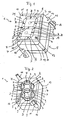
- a light guide component 1 for a 7-segment optical display with a decimal point is shown schematically.
- the optical waveguide component 1 consists of a cuboid main body 2 which forms a mask M with parallel channels K, the mask M corresponding in cross section to a 7-segment display with a decimal point.
- a light guide 3 with a segmental cross-sectional area and for the decimal point a light guide 4 is guided with a circular cross-sectional area from a light entrance side 5 to one of the light entrance side 5 opposite light exit side 6 for each of the seven segments of the 7-segment display ,
- the light guides 3, 4 open into a light-conducting plate 7, which is arranged on the base body 2 and has a planar surface 8.
- the light guides 3, 4 are in FIG. 1 shown by dashed lines, since they are below the photoconductive plate 7.
- Each of the segment-shaped light guides 3 has a width B and the circular light guide 4 has a diameter D, both of which are in particular less than or equal to one millimeter.
- the individual segmental light guides 3 are separated from one another by webs S of the mask M continuously from the light entrance side 5 to the light exit side 6.
- each locking element 11 On the main body 2, which is in particular cuboid, is arranged at two diagonally opposite corners of the Lichteintrittseite 5 associated rectangular surface each locking element 11 so that it starting from one of the associated, parallel to the optical fibers 3, 4 cuboid edge 10th protrudes beyond the light entry side 5 of the optical fiber component 1 and is freely movable.
- the base body 2 At the two remaining, parallel to the light guides 3, 4 edges 12, the base body 2 each have a line-shaped recess 13 which is formed form-fitting manner to the locking elements 11.
- the curvature 14 of the locking elements 11 corresponds in its negative shape of the curvature 15 of the recesses 13.
- another identical optical fiber component 1 can be arranged without gaps (not shown), since the locking element 11 fits into the recess 13 in a form-fitting manner.
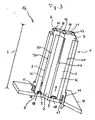
- FIG. 3 is a section along the light guides 3, 4 shown by an optical assembly 16, which is adapted for the optical 7-segment display.
- the optical assembly 16 includes the optical fiber device 1 and a printed circuit board 17 with SMD LEDs 18 as light-emitting components.
- the light guide component 1 is latched with its locking elements 11 in holes 19 of the circuit board 17.
- the SMD LEDs 18 are encompassed by the recesses 9 of the optical waveguide component 1, so that light emitted by the SMD LEDs can propagate along the optical waveguides 3, 4 only in the direction marked by arrows. Overcoupling of light of the SMD LED in adjacent light guides 3, 4 is avoided in that on the light entrance side 5, the light guide component 1 between the recesses 9 positively closes with the circuit board 17.
- These recesses 9 can be filled in particular with the use of SMD LED chips 18 without LED housing with a transparent potting compound, on the one hand protects the SMD LED chips 18 from damage and on the other hand, the light coupling of the emitted light in the light guide. 3 , 4, since the number of optical transitions is reduced and the transparent potting compound can be selected such that its optical refractive index is matched to that of the optical waveguide 3, 4.
- the recesses 9 can also be filled with diffuser material, by which light emitted by the SMD LEDs is scattered, so that the light enters the light guides 3, 4 with a uniform distribution. In general, other light-emitting components can be used, such as LEDs or incandescent lamps, the dimensions of the optical fiber component can be adjusted accordingly.
- an air gap 20 is formed in the channels K throughout the entire length L of the light guide 3, 4 from the light entrance side 5 to the light exit side 6, which is in particular of the order of microns.
- the light emitted by the SMD LED 18 and coupled on the light entrance side 5 in the light guide 3, 4 light that propagates in the light guide 3, 4 and which meets the air gap 20 in the light guide 3, 4 reflected back , In this way, the light is guided in the light guide 3, 4 and not absorbed by the base body 2.
- optical fibers 3, 4 with a long length L to keep the light losses low.
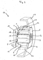
- FIG. 4 schematically shows a section along the light guide 3 through a shutter member 23 with an optical assembly 16 which is adapted according to a further embodiment of the invention for a multi-segment optical display.
- the light-conducting plate 7 extends in its planar extension beyond the base body 2 and has a curved shape, which is adapted to the curvature of the diaphragm part 23.
- the outer contour may, as shown, have a rectangular shape or any other desired shape.
- 7 latching elements 24 are integrally formed on the photoconductive plate 7, which are bounded on the light exit side 6 of the plate 7 and parallel to the light guide component 1 to the light entrance side 5 point.
- counter-locking elements 25 are formed, with which the latching elements 25 are latched for mounting the optical assembly 16 on the panel part 23.
- the optical fiber component 1 is manufactured in 2K injection molding technology from two plastic components (2K).
- the base body 2 with the mask M is made from an opaque, easily flowing material with a low volume shrinkage during the cooling process, which according to the invention is a liquid-crystalline polymer (LCP), such as Vectra®. Due to the processing properties of this liquid-crystalline polymer, the production of long and filigree masks M is possible.
- the light guide 3, 4 are injected from a second translucent plastic, which does not connect to the plastic of the mask M and according to the invention is a transparent amorphous plastic, in particular polymethylmethacrylate (PMMA).
- PMMA polymethylmethacrylate
- the PMMA has a lower melting point than LCP, so that the temperature of the PMMA melt during the manufacturing process can be chosen so that the mask M does not melt when injecting the PMMA as possible.
- the PMMA is injected via a ground pad P at the light exit side 6 in the mask M, which forms the photoconductive plate 7.
- FIG. 1 are centrally shown between the individual light guides 3 two injection points A in dotted lines through which the ground pad P is filled with PMMA. Starting from this mass cushion P, the PMMA is pressed into channels K of the mask M.
- a volume shrinkage occurs. This is very low for an LCP, such as Vectra®, while the volume shrinkage of PMMA is in the order of 0.6%.
- the volume shrinkage of the optical waveguide material compared to the mask material during the cooling process is significantly higher, resulting in a over the entire length L of the optical fibers 3, 4 continuous air gap 20 between optical fibers 3, 4 and mask M is formed.
- the formation of the air gap 20 largely independent of the manufacturing process, resulting in a high process reliability for the production of the optical fiber components 1.
- the optical waveguide component 1 can be manufactured with a ratio of length L to width B or diameter D of the optical waveguides 3, 4 which is greater than 13 or on the order of 30.
- the width B or the diameter D of the light guides 3, 4 may be less than or equal to 1 millimeter and the length L of the light guides 35 millimeters.
- a digit height of the 7-segment display of 10 millimeters can be realized with a segment width of 1 millimeter and an optical fiber length of 35 millimeters.
- other dimensions of the optical waveguide component 1 are also possible.
- the plastic for forming the light guides 3, 4 or the light-guiding plate 7 and / or the plastic for forming the main body 2 may be colored in itself.
- the light guides 3, 4 and the photoconductive plate 7 may be adapted in color to the panel part 23 or to a housing part such that segments of the multi-segment display are visible only when illuminated.
- the light-emitting components can be chosen such that they emit colored light, so that there is a color contrast between illuminated and unlit segments of the multi-segment display.
Landscapes
- Physics & Mathematics (AREA)
- General Physics & Mathematics (AREA)
- Engineering & Computer Science (AREA)
- Theoretical Computer Science (AREA)
- Optical Couplings Of Light Guides (AREA)
- Devices For Indicating Variable Information By Combining Individual Elements (AREA)
- Moulds For Moulding Plastics Or The Like (AREA)
- Injection Moulding Of Plastics Or The Like (AREA)
- Optical Fibers, Optical Fiber Cores, And Optical Fiber Bundles (AREA)
Claims (36)
- Composant de guide de lumière comprenant un côté d'entrée de la lumière (5) et un côté de sortie de la lumière (6) pour des dispositifs optiques d'affichage à segments multiples, lequel composant de guide de lumière présente un masque (M) dans lequel, pour chaque segment, un guide de lumière (3, 4) ayant une section en forme du segment est guidé, et lequel est fabriqué en technique d'injection par moulage à deux composants, caractérisé en ce qu'un espace d'air (20) est réalisé de manière continue entre le masque (M) et le guide de lumière (3, 4).
- Composant de guide de lumière selon la revendication 1, caractérisé en ce que l'espace d'air (20) présente une dimension dans la gamme des micromètres.
- Composant de guide de lumière selon la revendication 1 ou 2, caractérisé en ce que l'espace d'air (20) est formé par une perte de volume plus élevée du matériau du guide de lumière par rapport au matériau du masque lors du processus de refroidissement.
- Composant de guide de lumière selon l'une quelconque des revendications 1 à 3, caractérisé en ce que le matériau du masque et le matériau du guide de lumière ne se lient pas l'un à l'autre lors du processus de fabrication.
- Composant de guide de lumière selon l'une quelconque des revendications précédentes, caractérisé en ce que le matériau du guide de lumière ne fond pas le matériau du masque lors du processus de fabrication.
- Composant de guide de lumière selon l'une quelconque des revendications précédentes, caractérisé en ce que le matériau du masque est un matériau étanche à la lumière, à écoulement facile, ayant une perte de volume faible lors du processus de refroidissement.
- Composant de guide de lumière selon la revendication 6, caractérisé en ce que le matériau du masque est un polymère à cristaux liquides.
- Composant de guide de lumière selon l'une quelconque des revendications précédentes, caractérisé en ce que le matériau du guide de lumière est une matière plastique amorphe transparente.
- Composant de guide de lumière selon la revendication 8, caractérisé en ce que le matériau du guide de lumière est un polyméthacrylate de méthyle.
- Composant de guide de lumière selon l'une quelconque des revendications précédentes, caractérisé en ce que le rapport entre la longueur (L) et la largeur (B) ou le diamètre (D) du guide de lumière (3, 4) est supérieur à 13 ou se situe dans l'ordre de grandeur de 30.
- Composant de guide de lumière selon l'une quelconque des revendications précédentes, caractérisé en ce que la largeur (B) ou le diamètre (D) du guide de lumière (3, 4) est au maximum de 1 mm et/ou en ce que la longueur (L) du guide de lumière (3, 4) est de 35 mm.
- Composant de guide de lumière selon l'une quelconque des revendications précédentes, caractérisé en ce que le matériau du guide de lumière forme sur le côté de sortie de la lumière (6) une plaque (7) guidant la lumière.
- Composant de guide de lumière selon la revendication 12, caractérisé en ce que le guide de lumière (3, 4) de chaque segment est relié à la plaque (7).
- Composant de guide de lumière selon la revendication 12 ou 13, caractérisé en ce que la plaque (7) présente une surface rugueuse et/ou structurée (8, 21).
- Composant de guide de lumière selon l'une quelconque des revendications 12 à 14, caractérisé en ce que la plaque (7) dépasse latéralement au-delà du masque (2, M).
- Composant de guide de lumière selon l'une quelconque des revendications 12 à 15, caractérisé en ce que la plaque (7) est bombée de manière cylindrique ou sphérique.
- Composant de guide de lumière selon la revendication 16, caractérisé en ce que la forme de la plaque (7) est adaptée à un bandeau (23).
- Composant de guide de lumière selon l'une quelconque des revendications 12 à 17, caractérisé en ce que des éléments à crans (24) sont réalisés sur la plaque (7) pour fixer le composant de guide de lumière (1) sur une partie du boîtier et/ou sur une partie du bandeau (23).
- Composant de guide de lumière selon l'une quelconque des revendications précédentes, caractérisé en ce que le guide de lumière (3, 4) est poli sur le côté d'entrée de la lumière (5).
- Composant de guide de lumière selon l'une quelconque des revendications précédentes, caractérisé en ce que le composant de guide de lumière (1) présente pour chaque segment sur le côté d'entrée de la lumière (5) un évidement (9) destiné à entourer un composant émettant de la lumière (18).
- Composant de guide de lumière selon la revendication 20, caractérisé en ce que l'évidement (9) est réalisé pour entourer une LED SMD (18).
- Composant de guide de lumière selon l'une quelconque des revendications précédentes, caractérisé en ce que le masque (2, M) est en forme de parallélépipède rectangle et présente des éléments à crans (11) pour fixer le guide de lumière (1) sur une plaquette à circuit imprimé (17) et/ou sur une partie du boîtier.
- Composant de guide de lumière selon la revendication 22, caractérisé en ce que les éléments à crans (11) sont disposés sur le côté d'entrée de la lumière (5).
- Composant de guide de lumière selon la revendication 22 ou 23, caractérisé en ce que sur deux coins, opposés diagonalement l'un à l'autre, d'une surface de parallélépipède rectangle attribuée au côté d'entrée de la lumière (5), est respectivement disposé un élément à crans (11) de manière à ce que, partant d'une arête de parallélépipède rectangle (10) correspondante située parallèlement aux guides de lumière (3, 4), il soit dirigé de manière librement déplaçable en direction de la plaquette à circuit imprimé (17), et que les deux arêtes (12) restantes situées parallèlement aux guides de lumière (3, 4) présentent chacune un évidement (13) linéaire réalisé dans une forme négative par rapport à l'élément à crans (11), lequel évidement peut être assemblé par adhérence de forme à l'élément à crans (11) d'un guide de lumière voisin (1).
- Composant de guide de lumière selon l'une quelconque des revendications précédentes, caractérisé en ce que le matériau du guide de lumière et/ou le matériau du masque sont colorés en soi.
- Ensemble optique comprenant un composant de guide de lumière selon l'une quelconque des revendications 1 à 25, lequel est configuré pour un dispositif d'affichage à segments multiples.
- Ensemble optique selon la revendication 26, caractérisé en ce que le dispositif d'affichage à segments multiples est un dispositif d'affichage à 7 segments.
- Ensemble optique selon la revendication 26 ou 27, caractérisé en ce qu'il contient des LED SMD (18).
- Ensemble optique selon la revendication 28, caractérisé en ce que l'évidement (9) du composant de guide de lumière (1) qui entoure les LED SMD (18) est rempli avec une masse de remplissage transparente et/ou avec du matériau de diffusion.
- Ensemble optique selon la revendication 28 ou 29, caractérisé en ce que le composant de guide de lumière (1) est enclenché du côté d'entrée de la lumière (5) avec une plaquette à circuit imprimé (17) sur laquelle sont disposées les LED SMD (18).
- Appareil ménager qui présente un boîtier ou un bandeau (23) comprenant un ensemble optique (16) selon l'une quelconque des revendications 26 à 30.
- Appareil ménager selon la revendication 31, caractérisé en ce que la teinte des guides de lumière (3, 4) et/ou du masque (2, M) est adaptée au boîtier ou au bandeau (23).
- Appareil ménager selon la revendication 31 ou 32, caractérisé en ce que l'ensemble optique (16) est enclenché sur le boîtier ou sur le bandeau (23) au moyen d'éléments à crans (24) du composant de guide de lumière (1).
- Procédé de fabrication d'un composant de guide de lumière selon l'une quelconque des revendications 1 à 25 en technique de moulage par injection à deux composants, caractérisé en ce que les paramètres de fabrication sont adaptés à la température de fusion du matériau du masque de manière à ce qu'une fusion du matériau du masque soit réduite au minimum lors de l'injection du matériau du guide de lumière dans le masque (M).
- Procédé selon la revendication 34, caractérisé en ce que le matériau du guide de lumière est injecté dans le masque (M) par l'intermédiaire d'un coussin de masse sur le côté de sortie de la lumière.
- Procédé selon la revendication 35, caractérisé en ce qu'au moins un point d'injection (A) du matériau du guide de lumière est disposé entre les segments.
Applications Claiming Priority (2)
| Application Number | Priority Date | Filing Date | Title |
|---|---|---|---|
| DE10333316A DE10333316A1 (de) | 2003-07-22 | 2003-07-22 | Lichtleiterbauteil für optische Mehrsegmentsanzeigen |
| DE10333316 | 2003-07-22 |
Publications (3)
| Publication Number | Publication Date |
|---|---|
| EP1505560A2 EP1505560A2 (fr) | 2005-02-09 |
| EP1505560A3 EP1505560A3 (fr) | 2005-12-14 |
| EP1505560B1 true EP1505560B1 (fr) | 2012-03-07 |
Family
ID=33547032
Family Applications (1)
| Application Number | Title | Priority Date | Filing Date |
|---|---|---|---|
| EP04015509A Expired - Lifetime EP1505560B1 (fr) | 2003-07-22 | 2004-07-01 | Guide de lumière pour dispositifs d' affichage à segments multiples |
Country Status (4)
| Country | Link |
|---|---|
| EP (1) | EP1505560B1 (fr) |
| AT (1) | ATE548722T1 (fr) |
| DE (1) | DE10333316A1 (fr) |
| ES (1) | ES2380829T3 (fr) |
Families Citing this family (8)
| Publication number | Priority date | Publication date | Assignee | Title |
|---|---|---|---|---|
| DE102008061853A1 (de) * | 2008-12-15 | 2010-06-24 | Gigaset Communications Gmbh | Segmentanzeige mit einem Lichtleiter |
| DE102010025247A1 (de) * | 2010-06-26 | 2011-12-29 | Diehl Ako Stiftung & Co. Kg | Anzeigeeinrichtung |
| US8967834B2 (en) | 2012-05-23 | 2015-03-03 | Iluminage Beauty, Ltd. | Curved dead front display |
| US20130314642A1 (en) * | 2012-05-23 | 2013-11-28 | Conopco, Inc., D/B/A Unilever | Non-black dead front display |
| JP6618083B2 (ja) * | 2013-08-22 | 2019-12-11 | マッカーシー ミュージック コーポレイション | ピアノキーボードを備える装置 |
| FR3019258B1 (fr) | 2014-03-31 | 2019-04-05 | Valeo Vision | Guide de lumiere comportant une surface de sortie recouverte de matiere diffusante |
| DE102014213803A1 (de) * | 2014-07-16 | 2016-01-21 | BSH Hausgeräte GmbH | Anzeigevorrichtung und Haushaltsgerät mit einer solchen Anzeigevorrichtung |
| DE102019202831A1 (de) * | 2019-03-01 | 2020-09-03 | BSH Hausgeräte GmbH | Anzeigemittel mit einer Streufolie |
Family Cites Families (15)
| Publication number | Priority date | Publication date | Assignee | Title |
|---|---|---|---|---|
| JPS5114439B2 (fr) * | 1972-05-15 | 1976-05-10 | ||
| DE2542095A1 (de) * | 1975-09-20 | 1977-03-24 | Licentia Gmbh | Halbleiteranordnung fuer die ziffernanzeige |
| DE2707081A1 (de) * | 1977-02-18 | 1978-08-24 | Ackeret Design Studios | Optische zahlensegmentanzeige |
| DE4130844A1 (de) * | 1991-09-17 | 1993-03-18 | Ronkholz Karl Heinz | Alphanumerische anzeigeeinrichtung |
| DE9212999U1 (de) * | 1992-09-26 | 1992-12-03 | Klöckner-Moeller GmbH, 5300 Bonn | Vorrichtung zur Distanzüberbrückung des Lichtes einer Leuchtanzeige, insbesondere für Leuchtdioden... |
| JP2894582B2 (ja) * | 1993-12-17 | 1999-05-24 | ローム株式会社 | 発光装置 |
| DE29608845U1 (de) * | 1996-05-15 | 1996-11-28 | Siemens AG, 80333 München | Optische Anzeigevorrichtung für ein Kommunikationsendgerät |
| JPH10143095A (ja) * | 1996-11-06 | 1998-05-29 | Pfu Ltd | 発光ダイオード表示装置およびその製造方法 |
| JPH10254387A (ja) * | 1997-03-10 | 1998-09-25 | Sanyo Electric Co Ltd | セグメント型表示器 |
| JP2000075811A (ja) * | 1998-08-27 | 2000-03-14 | Fuji Electric Ind Co Ltd | 表示ユニット |
| DE19843836A1 (de) * | 1998-09-24 | 2000-03-30 | Annax Anzeigesysteme Gmbh | Anzeigetafel zur optischen Darstellung zweidimensionaler, gegenüber der Anzeigefläche in einer Richtung im wesentlichen gleichmäßig bewegter Abbildungen |
| DE19903587A1 (de) * | 1999-01-29 | 2000-08-03 | Bsh Bosch Siemens Hausgeraete | Optische Anzeigevorrichtung für elektrische Haushaltsgeräte |
| JP2004510207A (ja) * | 2000-09-29 | 2004-04-02 | ジーイー ファナック オートメーション ノースアメリカ, インコーポレイテッド | 光ファイバー装置 |
| DE10112640C1 (de) * | 2001-03-16 | 2002-12-19 | Diehl Ako Stiftung Gmbh & Co | Anzeigeeinrichtung |
| DE10155126B4 (de) * | 2001-11-09 | 2006-01-19 | Diehl Ako Stiftung & Co. Kg | Optischer Signalgeber, insbesondere in der Bedienblende eines Haushaltsgroßgerätes |
-
2003
- 2003-07-22 DE DE10333316A patent/DE10333316A1/de not_active Ceased
-
2004
- 2004-07-01 AT AT04015509T patent/ATE548722T1/de active
- 2004-07-01 EP EP04015509A patent/EP1505560B1/fr not_active Expired - Lifetime
- 2004-07-01 ES ES04015509T patent/ES2380829T3/es not_active Expired - Lifetime
Also Published As
| Publication number | Publication date |
|---|---|
| DE10333316A1 (de) | 2005-02-10 |
| ES2380829T3 (es) | 2012-05-18 |
| EP1505560A3 (fr) | 2005-12-14 |
| ATE548722T1 (de) | 2012-03-15 |
| EP1505560A2 (fr) | 2005-02-09 |
Similar Documents
| Publication | Publication Date | Title |
|---|---|---|
| DE3240942C2 (fr) | ||
| EP2847509B1 (fr) | Dispositif d'éclairage pour projecteur de véhicule à moteur | |
| DE69122075T2 (de) | Dünne Plattenleuchte | |
| EP0400176B1 (fr) | Procédé pour fixer un élément optique fixable sur une surface | |
| EP0939004B1 (fr) | Dispositif d'affichage pour un véhicule | |
| DE3533286C2 (fr) | ||
| EP2028510B1 (fr) | Dispositif d'éclairage, en particulier pour véhicules | |
| EP2177843B1 (fr) | Lamelle stockée et pouvant être pivotée dans une installation de lamelles dans un boîtier d'une tuyère d'air | |
| DE60009299T2 (de) | Aufnahme für eine anzeige in einem kraftfahrzeug | |
| AT518118B1 (de) | Beleuchtungseinheit für ein Kraftfahrzeug | |
| DE69918466T2 (de) | Beleuchtungsvorrichtung und verfahren zu ihrer herstellung | |
| EP1141623B1 (fr) | Source lumineuse a couplage lateral oblique de lumiere | |
| EP1072383A1 (fr) | Article de matière plastique moulé par injection à plusieurs composants comprenant une fonction d'affichage optique | |
| EP1505560B1 (fr) | Guide de lumière pour dispositifs d' affichage à segments multiples | |
| DE102015219586A1 (de) | Fahrzeugverglasung | |
| DE102013009791A1 (de) | Leuchtvorrichtung für ein Kraftfahrzeug und Verfahren zum Betreiben | |
| DE2542590A1 (de) | Anzeigevorrichtung | |
| DE19860697A1 (de) | Verfahren zur Herstellung eines flachen Lichtleitermoduls | |
| DE69701809T2 (de) | Lichtzerstreuende federnde verbindung zwischen lichtleitern | |
| DE202005014267U1 (de) | Fahrzeugleuchte mit einem Lichtleiter mit zentraler Lichteinkopplung | |
| EP2787276A1 (fr) | Agencement de conducteurs de lumière doté de deux éléments conducteurs de lumière | |
| WO2011131429A1 (fr) | Guide de lumière plan, luminaire et procédé de fabrication d'un guide de lumière plan | |
| DE19860696A1 (de) | Lichtquellenelement mit seitlicher schräger Lichteinkopplung | |
| DE10112640C1 (de) | Anzeigeeinrichtung | |
| EP2201414B1 (fr) | Article d'éclairage |
Legal Events
| Date | Code | Title | Description |
|---|---|---|---|
| PUAI | Public reference made under article 153(3) epc to a published international application that has entered the european phase |
Free format text: ORIGINAL CODE: 0009012 |
|
| AK | Designated contracting states |
Kind code of ref document: A2 Designated state(s): AT BE BG CH CY CZ DE DK EE ES FI FR GB GR HU IE IT LI LU MC NL PL PT RO SE SI SK TR |
|
| AX | Request for extension of the european patent |
Extension state: AL HR LT LV MK |
|
| PUAL | Search report despatched |
Free format text: ORIGINAL CODE: 0009013 |
|
| AK | Designated contracting states |
Kind code of ref document: A3 Designated state(s): AT BE BG CH CY CZ DE DK EE ES FI FR GB GR HU IE IT LI LU MC NL PL PT RO SE SI SK TR |
|
| AX | Request for extension of the european patent |
Extension state: AL HR LT LV MK |
|
| 17P | Request for examination filed |
Effective date: 20060614 |
|
| AKX | Designation fees paid |
Designated state(s): AT BE BG CH CY CZ DE DK EE ES FI FR GB GR HU IE IT LI LU MC NL PL PT RO SE SI SK TR |
|
| GRAP | Despatch of communication of intention to grant a patent |
Free format text: ORIGINAL CODE: EPIDOSNIGR1 |
|
| GRAS | Grant fee paid |
Free format text: ORIGINAL CODE: EPIDOSNIGR3 |
|
| GRAA | (expected) grant |
Free format text: ORIGINAL CODE: 0009210 |
|
| AK | Designated contracting states |
Kind code of ref document: B1 Designated state(s): AT BE BG CH CY CZ DE DK EE ES FI FR GB GR HU IE IT LI LU MC NL PL PT RO SE SI SK TR |
|
| REG | Reference to a national code |
Ref country code: GB Ref legal event code: FG4D Free format text: NOT ENGLISH |
|
| REG | Reference to a national code |
Ref country code: CH Ref legal event code: EP Ref country code: AT Ref legal event code: REF Ref document number: 548722 Country of ref document: AT Kind code of ref document: T Effective date: 20120315 |
|
| REG | Reference to a national code |
Ref country code: IE Ref legal event code: FG4D Free format text: LANGUAGE OF EP DOCUMENT: GERMAN |
|
| REG | Reference to a national code |
Ref country code: DE Ref legal event code: R096 Ref document number: 502004013350 Country of ref document: DE Effective date: 20120503 |
|
| REG | Reference to a national code |
Ref country code: ES Ref legal event code: FG2A Ref document number: 2380829 Country of ref document: ES Kind code of ref document: T3 Effective date: 20120518 |
|
| REG | Reference to a national code |
Ref country code: NL Ref legal event code: VDEP Effective date: 20120307 |
|
| PG25 | Lapsed in a contracting state [announced via postgrant information from national office to epo] |
Ref country code: NL Free format text: LAPSE BECAUSE OF FAILURE TO SUBMIT A TRANSLATION OF THE DESCRIPTION OR TO PAY THE FEE WITHIN THE PRESCRIBED TIME-LIMIT Effective date: 20120307 |
|
| PG25 | Lapsed in a contracting state [announced via postgrant information from national office to epo] |
Ref country code: FI Free format text: LAPSE BECAUSE OF FAILURE TO SUBMIT A TRANSLATION OF THE DESCRIPTION OR TO PAY THE FEE WITHIN THE PRESCRIBED TIME-LIMIT Effective date: 20120307 Ref country code: GR Free format text: LAPSE BECAUSE OF FAILURE TO SUBMIT A TRANSLATION OF THE DESCRIPTION OR TO PAY THE FEE WITHIN THE PRESCRIBED TIME-LIMIT Effective date: 20120608 |
|
| PG25 | Lapsed in a contracting state [announced via postgrant information from national office to epo] |
Ref country code: CY Free format text: LAPSE BECAUSE OF FAILURE TO SUBMIT A TRANSLATION OF THE DESCRIPTION OR TO PAY THE FEE WITHIN THE PRESCRIBED TIME-LIMIT Effective date: 20120307 |
|
| PG25 | Lapsed in a contracting state [announced via postgrant information from national office to epo] |
Ref country code: RO Free format text: LAPSE BECAUSE OF FAILURE TO SUBMIT A TRANSLATION OF THE DESCRIPTION OR TO PAY THE FEE WITHIN THE PRESCRIBED TIME-LIMIT Effective date: 20120307 Ref country code: SI Free format text: LAPSE BECAUSE OF FAILURE TO SUBMIT A TRANSLATION OF THE DESCRIPTION OR TO PAY THE FEE WITHIN THE PRESCRIBED TIME-LIMIT Effective date: 20120307 Ref country code: CZ Free format text: LAPSE BECAUSE OF FAILURE TO SUBMIT A TRANSLATION OF THE DESCRIPTION OR TO PAY THE FEE WITHIN THE PRESCRIBED TIME-LIMIT Effective date: 20120307 Ref country code: EE Free format text: LAPSE BECAUSE OF FAILURE TO SUBMIT A TRANSLATION OF THE DESCRIPTION OR TO PAY THE FEE WITHIN THE PRESCRIBED TIME-LIMIT Effective date: 20120307 Ref country code: SE Free format text: LAPSE BECAUSE OF FAILURE TO SUBMIT A TRANSLATION OF THE DESCRIPTION OR TO PAY THE FEE WITHIN THE PRESCRIBED TIME-LIMIT Effective date: 20120307 Ref country code: PL Free format text: LAPSE BECAUSE OF FAILURE TO SUBMIT A TRANSLATION OF THE DESCRIPTION OR TO PAY THE FEE WITHIN THE PRESCRIBED TIME-LIMIT Effective date: 20120307 |
|
| PG25 | Lapsed in a contracting state [announced via postgrant information from national office to epo] |
Ref country code: SK Free format text: LAPSE BECAUSE OF FAILURE TO SUBMIT A TRANSLATION OF THE DESCRIPTION OR TO PAY THE FEE WITHIN THE PRESCRIBED TIME-LIMIT Effective date: 20120307 Ref country code: PT Free format text: LAPSE BECAUSE OF FAILURE TO SUBMIT A TRANSLATION OF THE DESCRIPTION OR TO PAY THE FEE WITHIN THE PRESCRIBED TIME-LIMIT Effective date: 20120709 |
|
| PLBE | No opposition filed within time limit |
Free format text: ORIGINAL CODE: 0009261 |
|
| STAA | Information on the status of an ep patent application or granted ep patent |
Free format text: STATUS: NO OPPOSITION FILED WITHIN TIME LIMIT |
|
| BERE | Be: lapsed |
Owner name: BSH BOSCH UND SIEMENS HAUSGERATE G.M.B.H. Effective date: 20120731 |
|
| PG25 | Lapsed in a contracting state [announced via postgrant information from national office to epo] |
Ref country code: DK Free format text: LAPSE BECAUSE OF FAILURE TO SUBMIT A TRANSLATION OF THE DESCRIPTION OR TO PAY THE FEE WITHIN THE PRESCRIBED TIME-LIMIT Effective date: 20120307 |
|
| 26N | No opposition filed |
Effective date: 20121210 |
|
| PG25 | Lapsed in a contracting state [announced via postgrant information from national office to epo] |
Ref country code: MC Free format text: LAPSE BECAUSE OF NON-PAYMENT OF DUE FEES Effective date: 20120731 |
|
| REG | Reference to a national code |
Ref country code: CH Ref legal event code: PL |
|
| REG | Reference to a national code |
Ref country code: DE Ref legal event code: R097 Ref document number: 502004013350 Country of ref document: DE Effective date: 20121210 |
|
| PG25 | Lapsed in a contracting state [announced via postgrant information from national office to epo] |
Ref country code: CH Free format text: LAPSE BECAUSE OF NON-PAYMENT OF DUE FEES Effective date: 20120731 Ref country code: LI Free format text: LAPSE BECAUSE OF NON-PAYMENT OF DUE FEES Effective date: 20120731 |
|
| REG | Reference to a national code |
Ref country code: IE Ref legal event code: MM4A |
|
| PG25 | Lapsed in a contracting state [announced via postgrant information from national office to epo] |
Ref country code: BE Free format text: LAPSE BECAUSE OF NON-PAYMENT OF DUE FEES Effective date: 20120731 |
|
| PG25 | Lapsed in a contracting state [announced via postgrant information from national office to epo] |
Ref country code: IE Free format text: LAPSE BECAUSE OF NON-PAYMENT OF DUE FEES Effective date: 20120701 Ref country code: BG Free format text: LAPSE BECAUSE OF FAILURE TO SUBMIT A TRANSLATION OF THE DESCRIPTION OR TO PAY THE FEE WITHIN THE PRESCRIBED TIME-LIMIT Effective date: 20120607 |
|
| REG | Reference to a national code |
Ref country code: AT Ref legal event code: MM01 Ref document number: 548722 Country of ref document: AT Kind code of ref document: T Effective date: 20120731 |
|
| PG25 | Lapsed in a contracting state [announced via postgrant information from national office to epo] |
Ref country code: AT Free format text: LAPSE BECAUSE OF NON-PAYMENT OF DUE FEES Effective date: 20120731 |
|
| PG25 | Lapsed in a contracting state [announced via postgrant information from national office to epo] |
Ref country code: LU Free format text: LAPSE BECAUSE OF NON-PAYMENT OF DUE FEES Effective date: 20120701 |
|
| PG25 | Lapsed in a contracting state [announced via postgrant information from national office to epo] |
Ref country code: HU Free format text: LAPSE BECAUSE OF FAILURE TO SUBMIT A TRANSLATION OF THE DESCRIPTION OR TO PAY THE FEE WITHIN THE PRESCRIBED TIME-LIMIT Effective date: 20040701 |
|
| REG | Reference to a national code |
Ref country code: DE Ref legal event code: R081 Ref document number: 502004013350 Country of ref document: DE Owner name: BSH HAUSGERAETE GMBH, DE Free format text: FORMER OWNER: BSH BOSCH UND SIEMENS HAUSGERAETE GMBH, 81739 MUENCHEN, DE Effective date: 20150407 Ref country code: DE Ref legal event code: R081 Ref document number: 502004013350 Country of ref document: DE Owner name: BSH HAUSGERAETE GMBH, DE Free format text: FORMER OWNER: BSH BOSCH UND SIEMENS HAUSGERAETE GMBH, 81739 MUENCHEN, DE Effective date: 20120314 |
|
| REG | Reference to a national code |
Ref country code: ES Ref legal event code: PC2A Owner name: BSH HAUSGERATE GMBH Effective date: 20150527 |
|
| REG | Reference to a national code |
Ref country code: FR Ref legal event code: PLFP Year of fee payment: 12 |
|
| REG | Reference to a national code |
Ref country code: FR Ref legal event code: CD Owner name: BSH HAUSGERATE GMBH Effective date: 20151022 |
|
| REG | Reference to a national code |
Ref country code: FR Ref legal event code: PLFP Year of fee payment: 13 |
|
| REG | Reference to a national code |
Ref country code: FR Ref legal event code: PLFP Year of fee payment: 14 |
|
| REG | Reference to a national code |
Ref country code: FR Ref legal event code: PLFP Year of fee payment: 15 |
|
| PGFP | Annual fee paid to national office [announced via postgrant information from national office to epo] |
Ref country code: TR Payment date: 20230621 Year of fee payment: 20 |
|
| PGFP | Annual fee paid to national office [announced via postgrant information from national office to epo] |
Ref country code: IT Payment date: 20230731 Year of fee payment: 20 Ref country code: GB Payment date: 20230724 Year of fee payment: 20 Ref country code: ES Payment date: 20230821 Year of fee payment: 20 |
|
| PGFP | Annual fee paid to national office [announced via postgrant information from national office to epo] |
Ref country code: FR Payment date: 20230720 Year of fee payment: 20 Ref country code: DE Payment date: 20230731 Year of fee payment: 20 |
|
| REG | Reference to a national code |
Ref country code: DE Ref legal event code: R071 Ref document number: 502004013350 Country of ref document: DE |
|
| PG25 | Lapsed in a contracting state [announced via postgrant information from national office to epo] |
Ref country code: GB Free format text: LAPSE BECAUSE OF EXPIRATION OF PROTECTION Effective date: 20240630 |
|
| REG | Reference to a national code |
Ref country code: GB Ref legal event code: PE20 Expiry date: 20240630 |
|
| REG | Reference to a national code |
Ref country code: ES Ref legal event code: FD2A Effective date: 20240729 |
|
| PG25 | Lapsed in a contracting state [announced via postgrant information from national office to epo] |
Ref country code: GB Free format text: LAPSE BECAUSE OF EXPIRATION OF PROTECTION Effective date: 20240630 |
|
| PG25 | Lapsed in a contracting state [announced via postgrant information from national office to epo] |
Ref country code: ES Free format text: LAPSE BECAUSE OF EXPIRATION OF PROTECTION Effective date: 20240702 |
|
| PG25 | Lapsed in a contracting state [announced via postgrant information from national office to epo] |
Ref country code: ES Free format text: LAPSE BECAUSE OF EXPIRATION OF PROTECTION Effective date: 20240702 |