EP1505658A2 - Dispositif semi-conducteur de mémoire rémanente ayant une structure à double grille flottante et procédé pour sa fabrication - Google Patents
Dispositif semi-conducteur de mémoire rémanente ayant une structure à double grille flottante et procédé pour sa fabrication Download PDFInfo
- Publication number
- EP1505658A2 EP1505658A2 EP04254761A EP04254761A EP1505658A2 EP 1505658 A2 EP1505658 A2 EP 1505658A2 EP 04254761 A EP04254761 A EP 04254761A EP 04254761 A EP04254761 A EP 04254761A EP 1505658 A2 EP1505658 A2 EP 1505658A2
- Authority
- EP
- European Patent Office
- Prior art keywords
- floating gate
- word line
- active region
- disposed
- insulating layer
- Prior art date
- Legal status (The legal status is an assumption and is not a legal conclusion. Google has not performed a legal analysis and makes no representation as to the accuracy of the status listed.)
- Withdrawn
Links
Images








Classifications
-
- H—ELECTRICITY
- H10—SEMICONDUCTOR DEVICES; ELECTRIC SOLID-STATE DEVICES NOT OTHERWISE PROVIDED FOR
- H10B—ELECTRONIC MEMORY DEVICES
- H10B41/00—Electrically erasable-and-programmable ROM [EEPROM] devices comprising floating gates
- H10B41/30—Electrically erasable-and-programmable ROM [EEPROM] devices comprising floating gates characterised by the memory core region
-
- H—ELECTRICITY
- H10—SEMICONDUCTOR DEVICES; ELECTRIC SOLID-STATE DEVICES NOT OTHERWISE PROVIDED FOR
- H10B—ELECTRONIC MEMORY DEVICES
- H10B69/00—Erasable-and-programmable ROM [EPROM] devices not provided for in groups H10B41/00 - H10B63/00, e.g. ultraviolet erasable-and-programmable ROM [UVEPROM] devices
-
- H—ELECTRICITY
- H10—SEMICONDUCTOR DEVICES; ELECTRIC SOLID-STATE DEVICES NOT OTHERWISE PROVIDED FOR
- H10D—INORGANIC ELECTRIC SEMICONDUCTOR DEVICES
- H10D30/00—Field-effect transistors [FET]
- H10D30/01—Manufacture or treatment
- H10D30/021—Manufacture or treatment of FETs having insulated gates [IGFET]
- H10D30/0411—Manufacture or treatment of FETs having insulated gates [IGFET] of FETs having floating gates
-
- H—ELECTRICITY
- H10—SEMICONDUCTOR DEVICES; ELECTRIC SOLID-STATE DEVICES NOT OTHERWISE PROVIDED FOR
- H10D—INORGANIC ELECTRIC SEMICONDUCTOR DEVICES
- H10D30/00—Field-effect transistors [FET]
- H10D30/60—Insulated-gate field-effect transistors [IGFET]
- H10D30/68—Floating-gate IGFETs
- H10D30/681—Floating-gate IGFETs having only two programming levels
-
- H—ELECTRICITY
- H10—SEMICONDUCTOR DEVICES; ELECTRIC SOLID-STATE DEVICES NOT OTHERWISE PROVIDED FOR
- H10D—INORGANIC ELECTRIC SEMICONDUCTOR DEVICES
- H10D30/00—Field-effect transistors [FET]
- H10D30/60—Insulated-gate field-effect transistors [IGFET]
- H10D30/68—Floating-gate IGFETs
- H10D30/687—Floating-gate IGFETs having more than two programming levels
-
- H—ELECTRICITY
- H10—SEMICONDUCTOR DEVICES; ELECTRIC SOLID-STATE DEVICES NOT OTHERWISE PROVIDED FOR
- H10D—INORGANIC ELECTRIC SEMICONDUCTOR DEVICES
- H10D30/00—Field-effect transistors [FET]
- H10D30/60—Insulated-gate field-effect transistors [IGFET]
- H10D30/68—Floating-gate IGFETs
- H10D30/6891—Floating-gate IGFETs characterised by the shapes, relative sizes or dispositions of the floating gate electrode
-
- H—ELECTRICITY
- H10—SEMICONDUCTOR DEVICES; ELECTRIC SOLID-STATE DEVICES NOT OTHERWISE PROVIDED FOR
- H10D—INORGANIC ELECTRIC SEMICONDUCTOR DEVICES
- H10D64/00—Electrodes of devices having potential barriers
- H10D64/01—Manufacture or treatment
- H10D64/031—Manufacture or treatment of data-storage electrodes
- H10D64/035—Manufacture or treatment of data-storage electrodes comprising conductor-insulator-conductor-insulator-semiconductor structures
-
- H—ELECTRICITY
- H10—SEMICONDUCTOR DEVICES; ELECTRIC SOLID-STATE DEVICES NOT OTHERWISE PROVIDED FOR
- H10D—INORGANIC ELECTRIC SEMICONDUCTOR DEVICES
- H10D86/00—Integrated devices formed in or on insulating or conducting substrates, e.g. formed in silicon-on-insulator [SOI] substrates or on stainless steel or glass substrates
- H10D86/01—Manufacture or treatment
- H10D86/011—Manufacture or treatment comprising FinFETs
-
- H—ELECTRICITY
- H10—SEMICONDUCTOR DEVICES; ELECTRIC SOLID-STATE DEVICES NOT OTHERWISE PROVIDED FOR
- H10D—INORGANIC ELECTRIC SEMICONDUCTOR DEVICES
- H10D86/00—Integrated devices formed in or on insulating or conducting substrates, e.g. formed in silicon-on-insulator [SOI] substrates or on stainless steel or glass substrates
- H10D86/201—Integrated devices formed in or on insulating or conducting substrates, e.g. formed in silicon-on-insulator [SOI] substrates or on stainless steel or glass substrates the substrates comprising an insulating layer on a semiconductor body, e.g. SOI
- H10D86/215—Integrated devices formed in or on insulating or conducting substrates, e.g. formed in silicon-on-insulator [SOI] substrates or on stainless steel or glass substrates the substrates comprising an insulating layer on a semiconductor body, e.g. SOI comprising FinFETs
-
- H—ELECTRICITY
- H10—SEMICONDUCTOR DEVICES; ELECTRIC SOLID-STATE DEVICES NOT OTHERWISE PROVIDED FOR
- H10D—INORGANIC ELECTRIC SEMICONDUCTOR DEVICES
- H10D30/00—Field-effect transistors [FET]
- H10D30/01—Manufacture or treatment
- H10D30/021—Manufacture or treatment of FETs having insulated gates [IGFET]
- H10D30/024—Manufacture or treatment of FETs having insulated gates [IGFET] of fin field-effect transistors [FinFET]
-
- H—ELECTRICITY
- H10—SEMICONDUCTOR DEVICES; ELECTRIC SOLID-STATE DEVICES NOT OTHERWISE PROVIDED FOR
- H10D—INORGANIC ELECTRIC SEMICONDUCTOR DEVICES
- H10D30/00—Field-effect transistors [FET]
- H10D30/60—Insulated-gate field-effect transistors [IGFET]
- H10D30/62—Fin field-effect transistors [FinFET]
Definitions
- the present invention relates to a semiconductor memory device and a method of manufacturing the same. More particularly, the present invention relates to a non-planar split-gate-type nonvolatile semiconductor memory device and a method of manufacturing the same.
- EEPROM electrically erasable and programmable read only memory
- flash memory devices have become strongly relied upon.
- a flash memory widely used nowadays, can be electrically erased and programmed, and retains data even if the supply of power is interrupted.
- a nonvolatile semiconductor memory device memory cells are connected to a bit line parallel to each other. If the threshold voltage of a memory cell transistor becomes lower than a voltage (normally, 0 V) applied to a control gate of a non-selection memory cell, current flows between a source region and a drain region irrespective of whether a selection memory cell is turned on or off. As a result, all the memory cells are read as if they are continuously in a turn-on state. For this reason, it is necessary to strictly control the threshold voltage in the nonvolatile memory device, which is very difficult.
- a voltage normally, 0 V
- split-gate-type nonvolatile semiconductor memory devices e.g., as disclosed in U.S. Patent No. 5,045,488, have been proposed.
- a channel region formed by a floating gate and another channel region formed by a control gate are connected in series on the same plane.
- FET field effect transistor
- devices are scaled down, thereby achieving high efficiency and thus improving the operating speed.
- the channel length of an FET has been scaled down on the level of 100 nm or less, it is very difficult to sufficiently reduce the gate length of the FET by scaling.
- the conventional split-gate-type nonvolatile memory device has a planar channel structure. In this planar FET, the gate length can be scaled along with the scaling of a transistor.
- the distance between a source region and a drain region decreases, it is difficult to sufficiently scale a tunneling oxide layer.
- a split-gate-type flash memory device has a floating gate which is separated from a control gate and electrically isolated from the outside. Data storage is enabled by using a variation of current level in memory cells through injection of electrons into the floating gate (i.e., programming) and emission of the electrons from the floating gate (i.e., erasing).
- the injection of electrons into the floating gate is performed using channel hot electron injection (CHEI), whereas the emission of electrons from the floating gate is performed by F-N tunneling mechanism using an insulating layer between the floating gate and a control gate.
- CHEI channel hot electron injection
- F-N tunneling mechanism using an insulating layer between the floating gate and a control gate.
- Embodiments of the present invention provide a nonvolatile semiconductor memory device.
- the device is structured such that the short channel effect (SCE) is easily controlled to improve the scaling effect.
- the active region is a non-planar silicon structure with floating gates disposed on opposite sides of the active region.
- the device is structured such that the number of corners of a floating gate, where tips may be formed is increased.
- a control gate overlaps at least three corners of each floating gate.
- embodiments of the present invention may also provide a non-planar full depletion mode nonvolatile semiconductor memory device having a double-floating gate channel. Even though the distance between a source region and a drain region decreases due to scaling, the device of the present invention facilitates the control of a gate by increasing coupling between a channel and a floating gate, while reducing adverse coupling between the channel and the source or the drain.
- Embodiments of the present invention may further provide a method of manufacturing a nonvolatile semiconductor memory device. At least one embodiment of this method enhances the scaling effect and improves the current characteristics of cells by increasing the effective channel width per cell.
- FIG. 1 illustrates a perspective view of a nonvolatile semiconductor memory device according to an embodiment of the present invention. Specifically, FIG. 1 illustrates a 4-bit memory cell, in which one bit is comprised of a portion denoted by reference character "A".
- the nonvolatile semiconductor memory device of the present invention is formed on a buried oxide layer (BOX) 10 disposed on a silicon on insulator (SOI) substrate.
- the SOI substrate is made of a substrate formed by, for example, separation by implantation of oxygen (SIMOX), and the BOX 10 has a thickness of, for example, about 1000 ⁇ to 1500 ⁇ .
- the nonvolatile semiconductor memory device of the present invention comprises active regions, each of which includes a silicon island 20 obtained by patterning an SOI layer of the SOI substrate.
- the silicon island 20 has a thickness of about 500 ⁇ and extends in an x direction on the BOX 10 in the shape of a roughly square sectional bar.
- the silicon island 20 has a top surface that extends parallel to a main surface of the SOI substrate (i.e., the BOX 10) and two sidewalls that extend perpendicular to the main surface of the SOI substrate (i.e., the BOX 10).
- a channel region 22 is formed inside the silicon island 20 and extends in the x direction.
- a source line 30 is formed on a source 24 disposed inside the silicon island 20, adjacent to the channel region 22, and extends perpendicular to the lengthwise direction (i.e., the x direction) of the silicon island 20 (i.e., extends in a y direction).
- a bit line that extends in the x direction is connected to a drain 26 disposed adjacent the channel region 22.
- the memory cell is an NMOS device
- the silicon island 20 is doped with p-type impurity ions
- the source 24 and the drain 26 are doped with high-concentration n-type impurity ions.
- a pair of floating gates i.e., a first floating gate 42 and a second floating gate 44, which face each other with the silicon island 20 therebetween, are disposed adjacent to the channel region 22 of the silicon island 20.
- a first coupling gate insulating layer 52 is interposed between the channel region 22 and the first floating gate 42, and a second coupling gate insulating layer 54 is interposed between the channel region 22 and the second floating gate 44.
- the first floating gate 42 is electrically isolated from the second floating gate 44.
- a word line 60 covers the channel region 22 adjacent to the first floating gate 42 or the second floating gate 44 and extends in the y direction.
- a first interpoly tunneling insulating layer 56a is interposed between the first floating gate 42 and the word line 60
- a second interpoly tunneling insulating layer 56b is interposed between the second floating gate 44 and the word line 60.
- an insulating layer 58 is interposed between the channel region 22 and the word line 60. That is, the word line 60 includes a portion that faces the channel region 22 with the insulating layer 58 therebetween.
- a single memory cell, i.e., the portion A is defined only by a contact point between a single bit line, which are connected to the drain 26, and a single word line.
- the nonvolatile semiconductor memory device of embodiments of the present invention comprises a plurality of memory cells as shown in FIG. 1, each of which includes a pair of floating gates, i.e., the first floating gate 42 and the second floating gate 44.
- FIG. 1 each of which includes a pair of floating gates, i.e., the first floating gate 42 and the second floating gate 44.
- FIG. 2 is an enlarged perspective view of one memory cell, i.e., the portion "A" of FIG. 1, showing the channel region 22, the first floating gate 42, the second floating gate 44, and the word line 60.
- the word line 60 may be formed to surround corners 42a, 42b, 42c, and 42d of the first floating gate 42 and corners 44a, 44b, 44c, and 44d of the second floating gate 44 around the channel region 22.
- the first floating gate 42 and the second floating gate 44 have a first overlap portion 42s and a second overlap portion 44s, respectively, which overlap the word line 60.
- first floating gate 42 and the second floating gate 44 each have four corners that are surrounded by the word line 60 at the first overlap portion 42s and the second overlap portion 44s
- embodiments of the present invention are not limited thereto.
- the first floating gate 42 and the second floating gate 44 each may have at least three corners that are surrounded by the word line 60 at the first overlap portion 42s and the second overlap portion 44s.
- the word line 60 includes recessed surfaces 60a and 60b, which are respectively recessed for the word line 60 so as to surround the first overlap portion 42s and the second overlap portion 44s.
- the first interpoly tunneling insulating layer 56a is interposed between the word line 60 and the first overlap portion 42s to surround the corners 42a, 42b, 42c, and 42d of the first floating gate 42
- the second interpoly tunneling insulating layer 56b is interposed between the word line 60 and the second overlap portion 44s to surround the corners 44a, 44b, 44c, and 44d of the second floating gate 44.
- the insulating layer 58 is formed between the first overlap portion 42s and the second overlap portion 44s on the channel region 22.
- the nonvolatile memory device of embodiments of the present invention comprises two floating gates for a single memory cell, and a control gate formed of the word line 60. Accordingly, a split-gate-type nonvolatile semiconductor memory device having double floating gates in a single memory cell is provided.
- the thickness of a silicon body where a channel is formed should be about 1/3 the gate length of the silicon body to form a full depletion mode transistor (IEDM Tech. Digest, pp. 621-624, 2001, by R. Chau et al.).
- the nonvolatile semiconductor memory device of embodiments of the present invention has a double-floating gate structure, in which a single memory cell includes two floating gates. Accordingly, considering the thickness of the silicon island 20 that is controlled by each of the first and second floating gates 42 and 44, the width L s of the top surface of the silicon island 20 formed of the SOI layer may be set about 2/3 the x-directional length L fg of each of the first and second floating gates 42 and 44.
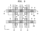
- FIG. 3 is a layout of the nonvolatile semiconductor memory device shown in FIG. 1.
- reference numeral 20A denotes an active region defined by the silicon island 20, 32 denotes a contact between the source 24 formed in the active region 20A and the source line 30, and 72 denotes a contact between the drain 26 formed in the active region 20A and a bit line 70.
- a portion B denotes a single memory cell corresponding to the portion A in FIG. 1.
- the nonvolatile semiconductor memory device of embodiments of the present invention comprises a plurality of island-shaped active regions 20A, which are formed on a BOX 10 disposed on a substrate and each of which includes two memory cells.
- the two memory cell have one source 24, i.e., one source line 30, in common inside one active region 20A.
- the word line 60 is connected to a series of memory cells, which respectively include a series of channel regions 22 disposed in the lengthwise direction of the word line 60, i.e., in the y direction, among channel regions 22 that are respectively formed in the plurality of active regions 20A. Also, a series of sources 24, which are formed inside a series of active regions 20A disposed in the lengthwise direction of the word line 60, i.e., in the y direction, are connected to each other via the source line 30.
- the first floating gate 42 and the second floating gate 44 each are formed of doped polysilicon or metal.
- the word line 60 and the source line 30 each are formed of doped polysilicon or metal and at least one of them may include a metal silicide layer.
- the metal silicide layer may be formed of, for example, cobalt silicide, nickel silicide, titanium silicide, hafnium silicide, platinum silicide, or tungsten silicide.
- the programming of memory cells is performed using a CHEI method.
- a CHEI method For example, when the memory cell is in an UV-erased initial state, if a high voltage is applied to the word line 60 of the memory cell and a high voltage is applied to the source 24 via the source line 30, two electron channels are formed on both sidewalls of the silicon island 20, which face the first and second floating gates 42 and 44, respectively, due to the threshold voltage Vth applied to the word line 60.
- Vth applied to the word line 60.
- channel hot carriers are generated to allow hot electrons to flow through the first and second coupling gate insulating layers 52 and 54 into the first and second floating gates 42 and 44.
- the first and second floating gates 42 and 44 are charged with negative charges.
- the first and second floating gates 42 and 44 each are charged to induce a negative voltage.
- the channels which are formed on the both sidewalls of the silicon island 20 that face the first and second floating gates 42 and 44, respectively, have an increased threshold voltage Vth, which differs from a voltage in the erased state.
- the erasing of the memory cell is performed using F-N tunneling, which involves the first and second interpoly tunneling insulating layers 56a and 56b between the first and second floating gates 42 and 44 and the control gate comprised of the word line 60.
- F-N tunneling involves the first and second interpoly tunneling insulating layers 56a and 56b between the first and second floating gates 42 and 44 and the control gate comprised of the word line 60.
- a high voltage is applied to the word line 60 and a low voltage is applied to the source 24.
- a strong electric field is induced in portions surrounding the overlap portions 42s and 44s of the first and second floating gates 42 and 44 of the word line 60, i.e., adjacent to the recessed surfaces 60a and 60b, due to the corners 42a, 42b, 42c, and 42d of the first floating gate 42 and the corners 44a, 44b, 44c, and 44d of the second floating gate 44.
- the strong electric field which concentrates in the corners 42a, 42b, 42c, 42d, 44a, 44b, 44c, and 44d of the first and second floating gates 42 and 44, is sufficiently capable of tunneling the electrons stored in the first and second floating gates 42 and 44 into the word line 60.
- the first and second floating gates 42 and 44 are placed in an initial state, i.e., an UV-erased state. Then, the channels formed on both sidewalls of the channel region 22 that face the first and second floating gates 42 and 44 have a lower threshold voltage than that when the programming is completed, thus allowing a relatively large current to flow during the reading operation.
- the nonvolatile semiconductor memory device of embodiments of the present invention is a non-planar split-gate-type device, which is formed on the SOI substrate, and each memory cell includes two floating gates 42 and 44 which are adjacent to both sidewalls of the active region, i.e., the silicon island 20.
- each of the floating gates 42 and 44 has at least three corners, into which the electric field can concentrate adjacent to the word line 60. That is, a total of six or more corners of the floating gates 42 and 44 are adjacent to the word line 60. Therefore, the number of F-N tunneling regions increases.
- both sidewalls of the active region 20 serve as the channels so as to increase the effective channel width for each cell in the layout. As a result, a large current can be held in the memory cell.
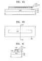
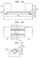
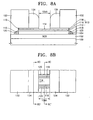
- FIGs. 4A, 4B, and 4C through 16A and 16B illustrate process steps of a method of manufacturing the nonvolatile semiconductor memory device shown in FIG. 1.
- FIGs. 4A through 16A are sectional views taken along line 4A-4A' of FIG. 3
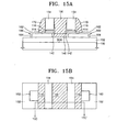
- FIGs. 4B through 15B are plan views of FIGs. 4A through 15A, respectively.
- FIGs. 4C through 15C are partial sectional views of FIGs. 4B through 15B, respectively
- FIGs. 8D through 14D and 14E are partial sectional views of FIGs. 8B through 14B, respectively.
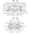
- FIG. 16B is a partial sectional view of FIG. 16A.
- an SOI substrate where a silicon substrate 100, a BOX 102, and an SOI layer are sequentially stacked is prepared.
- the SOI substrate may be formed by, for example, an SIMOX process.
- the BOX 102 has a thickness of about 1000 ⁇ to 1500 ⁇
- the SOI layer has a thickness of about 500 ⁇ .
- a mask pattern 110 is formed on the SOI layer to define an active region.
- the mask pattern 110 is formed of an oxide layer 112, a nitride layer 114, and another oxide layer 116, which are sequentially stacked.
- the oxide layer 112, the nitride layer 114, and the oxide layer 116 have a thickness of 200 ⁇ , 300 ⁇ , and 200 ⁇ , respectively.
- the SOI layer is anisotropically etched using the mask pattern 110 as an etch mask to form a silicon island 104.
- the silicon island 104 extends in a first direction, i.e., in the x direction shown in FIG. 1, in the shape of a substantially square sectional bar.
- the silicon island 104 has a top surface 104t, which extends parallel to a main surface of the BOX 102, and both sidewalls 104s extend from the BOX 102 perpendicular to the main surface of the BOX 102.
- FIGs. 5A, 5B, and 5C which is a sectional view taken along line 5C - 5C' of FIG. 5B, the exposed both sidewalls 104s of the silicon island 104 are covered with a first oxide layer 118 having a thickness of about 70 ⁇ . A portion of the first oxide layer 118 will constitute a coupling gate insulating layer later.
- the first oxide layer 118 may be formed using thermal oxidation, chemical vapor deposition (CVD), or a combination thereof.
- channel ion implantation is performed to dope the silicon island 104 with impurity ions of a first conductivity type, e.g., p-type impurity ions.
- a blanket conductive layer is formed to a thickness of about 400 ⁇ on the BOX 102 to cover the mask pattern 110 and the first oxide layer 118. Then, the blanket conductive layer is anisotropically etched using the mask pattern 110 and the BOX 102 as an etch stop layer to form a first conductive layer 120.
- the first conductive layer 120 faces the sidewalls 104s of the silicon island 104 on the first oxide layer 118, and surrounds the silicon island 104 in the shape of a spacer sidewall.
- the blanket conductive layer is anisotropically etched to form the first conductive layer 120, but the present invention is not limited thereto.
- the first conductive layer 120 may be formed using other methods, for example, by processing the blanket conductive layer using a photolithography process and chemical mechanical polishing (CMP).
- CMP chemical mechanical polishing
- the first conductive layer 120 is formed to have a square sectional shape having four corners instead of a shape having three corners (and a fourth rounded corner) as shown in FIG. 6A.
- the first conductive layer 120 may be formed of doped polysilicon or metal. To form the first conductive layer 120 using doped polysilicon, an undoped polysilicon may be deposited first and then doped with impurity ions, or an already doped polysilicon layer may be deposited.
- a silicon nitride layer having a thickness of about 1000 ⁇ is formed on the BOX 102 to cover the resultant structure where the first conductive layer 120 is formed. Thereafter, the silicon nitride layer is patterned using a photolithography process so as to expose the first conductive layer 120 in a central portion of the silicon island 104, i.e., a region where two floating gates and a source will be formed. Thus, a first protecting insulating pattern 132 is formed to protect a portion of the first conductive layer 120.
- a silicon oxide layer is formed to a thickness of about 1000 ⁇ on the entire surface of the resultant structure where the first protecting insulating pattern 132 is formed. Thereafter, the silicon oxide layer is anisotropically etched again to form a second protecting insulating pattern 134 on the sidewalls of the first protecting insulating pattern 132 in the shape of spacers. While the silicon oxide layer is being anisotropically etched to form the second protecting insulating pattern 134, the oxide layer 116 constituting an uppermost portion of the mask pattern 110 is also etched.
- the second protecting insulating pattern 134 covers and protects a portion of the first conductive layer 120, where floating gates will be formed. Also, the first conductive layer 120, which surrounds the silicon island 104, is exposed between the two adjacent second protecting insulating patterns 134.
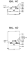
- FIGs. 8C and 8D are sectional views taken along lines 8C - 8C' and 8D - 8D', respectively, of FIG. 8B.
- first conductive layer 120 which covers the sidewalls of the silicon island 104 in the first region 104A, is selectively removed by using the first protecting insulating pattern 132 and the second protecting insulating pattern 134 as an etch mask.
- first exposed sidewalls 120a are formed adjacent to the first region 104A on the first conductive layer 120, and the first oxide layer 118 covering the sidewalls of the silicon island 104 is exposed in the first region 104A.
- the nitride layer 114 which is exposed on the silicon island 104, is removed in the first region 104A to expose the oxide layer 112 of the mask pattern 110 in the first region 104A.
- the first exposed sidewalls 120a disposed on the first conductive layer 120 are oxidized by thermal oxidation.
- a second oxide layer is formed by CVD on the resultant structure and then anisotropically etched again. This forms first insulating spacers 142 to cover the first exposed sidewalls 120a disposed on the first conductive layer 120.
- the thermal oxidation, for oxidizing the first exposed sidewalls 120a may be optionally omitted.
- spacers 144 are formed to cover the both sidewalls of the silicon island 104 in the first region 104A.
- the oxide layer 112 disposed on the silicon island 104 in the first region 104A is removed to expose the top surface of the silicon island 104.
- a source contact will be formed on the exposed top surface of the silicon island 104 later.
- the etching of the second oxide layer may be further performed to expose the both sidewalls of the silicon island 104, such that even the spacers 144 covering the both sidewalls of the silicon island 104 are removed in the first region 104A.
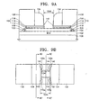
- FIGs. 9C and 9D are sectional views taken along lines 9C - 9C' and 9D - 9D', respectively, of FIG. 9B.
- impurity ions are implanted into the entire surface of the resultant structure to form a source 146 in the first region 104A of the silicon island 104.
- impurity ions of a second conductivity type which is opposite to the first conductivity type, e.g., n-type impurity ions, are implanted at a high concentration.
- the impurity ions for the source 146 are implanted at a higher concentration than that of the impurity ions for the channel ion implantation.
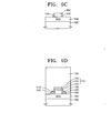
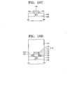
- FIGs. 10C and 10D are sectional views taken along lines 10C - 10C' and 10D - 10D', respectively, of FIG. 10B.
- a conductive material is deposited on the entire surface of the resultant structure where the source 146 is formed.
- a second conductive layer is formed to a thickness of about 3000 ⁇ to completely fill a space between the two adjacent second protecting insulating patterns 134 in the first region 104A.
- the second conductive layer is then planarized using CMP to form a source line 150 connected to the source 146.
- the source line 150 extends in a second direction, i.e., in the y direction, perpendicular to the first direction.
- the first protecting insulating pattern 132 and the second protecting insulating pattern 134 which are adjacent to the source line 150, have a slightly reduced height.
- the source line 150 forms an ohmic contact with the source 146.
- the second conductive layer which is used to form the source line 150, may be formed of doped polysilicon or metal.
- an undoped polysilicon layer may be deposited and then doped with impurity ions, or an already doped polysilicon layer may be deposited.
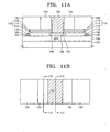
- FIGs. 11 C and 11D are sectional views taken along lines 11C - 11C' and 11 D - 11D', respectively, of FIG. 11B.
- the top surface of the source line 150 is thermally oxidized to form a thermal oxide layer 152 having a thickness of about 100 ⁇ .
- the first protecting insulating pattern 132 which is formed of the silicon nitride layer, is wet or dry etched and removed by using the thermal oxide layer 152 and the second protecting insulating pattern 134 as an etch mask.
- the oxide layer 116 of the mask pattern 110 which covers the top surface of the silicon island 104, is exposed in a second region 104B of the silicon island 104, and portions of the first conductive layer 120 and the BOX 102.
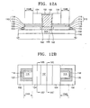
- FIGs. 12C and 12D are sectional views taken along lines 12C - 12C' and 12D - 12D', respectively, of FIG. 12B.
- a portion of the first conductive layer 120 which covers the second region 104B of the silicon island 104, is selectively removed by a dry or wet etching process using oxide layers exposed on the silicon substrate 100, i.e., the thermal oxide layer 152, the second protecting insulating pattern 134, the oxide layer 116, the first oxide layer 118, and the BOX 102 as a hard mask.
- a first floating gate 122 and a second floating gate 124 which are formed of the remaining portion of the first conductive layer 120, are formed under the second protecting insulating pattern 134.
- the first floating gate 122 and the second floating gate 124 face each other with the silicon island 104 disposed therebetween.
- second exposed sidewalls 120b are formed adjacent to the second region 104B on the remaining first conductive layer 120, i.e., the first and second floating gates 122 and 124.
- the second protecting insulating pattern 134 protects a portion of the first conductive layer 120, which remains adjacent the silicon island 104 excluding the first region 104A and the second region 104B.
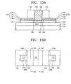
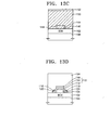
- FIGs. 13C and 13D are sectional views taken along lines 13C - 13C' and 13D - 13D', respectively, of FIG. 13B.
- the thermal oxide layer 152 and the oxide layer 116 of the mask pattern 110 are wet etched and removed to expose the nitride layer 114 of the mask pattern 110.
- the exposed nitride layer 114 is wet etched and removed to expose the oxide layer 112 of the mask pattern 110.
- the oxide layer 112 of the mask pattern 110 is wet etched and removed to expose the top surface of the silicon island 104 in the second region 104B.
- the second protecting insulating pattern 134 has reduced height and width.
- a portion of the top surfaces of the first and second floating gates 122 and 124, which is covered with the second protecting insulating pattern 134 is exposed by a predetermined width adjacent to the second protecting insulating pattern 134. That is, while the top surface of the silicon island 104 is being exposed in the second region 104B, the top surface 120c of the first and second floating gates 122 and 124 and the corners of the second exposed sidewalls 120b are exposed.
- a third oxide layer 160 is formed on the exposed top surface of the silicon island 104, the second exposed sidewalls 120b and the exposed top surface 120c of the first conductive layer 120 by using thermal oxidation or a CVD process.
- an insulating layer 162 is formed on the silicon island 104, and second insulating spacers 164a and 164b are formed on the second exposed sidewalls 120b and the exposed top surface 120c of the first conductive layer 120, which constitutes the first and second floating gates 122 and 124.
- the insulating layer 162 and the insulating spacers 164a and 164b are formed of the third oxide layer 160.
- the third oxide layer 160 may be formed to a thickness of about 160 ⁇ to 170 ⁇ , using thermal oxidation, a CVD process, or a combination thereof.
- the insulating layer 162 and the second insulating spacers 164a and 164b are concurrently formed.
- the second insulating spacers 164a and 164b are formed to cover the corners of the first floating gate 122 and the second floating gate 124, respectively.
- the second insulating spacers 164a and 164b function as a first interpoly tunneling insulating layer 164a and a second interpoly tunneling insulating layer 164b between the first floating gate 122 and a word line, which will be formed later, and between the second floating gate 124 and the word line.
- the same reference numerals are used to denote the second insulating spacers and the first and second interpoly tunneling insulating layers.
- the second insulating spacers 164a and 164b are formed on not only the second exposed sidewalls 120b of the first conductive layer 120 but also on the exposed surfaces 120c thereof, but the present invention is not limited thereto. That is, it is possible to control the areas of the exposed top surface 120c by varying the width of the second protecting insulating pattern 134, and it is also possible to form the second insulating spacers only on the second exposed sidewalls 120b without exposing the top surfaces of the first conductive layer 120.
- the width of the second protecting insulating pattern 134 is reduced so as to expose a portion of the top surface of the first conductive layer 120.
- FIGs. 14C and 14D are sectional views taken along lines 14C - 14C' and 14D - 14D', respectively, of FIG. 14B, and FIG. 14E is a sectional view taken along line 14E - 14E' of FIG. 14B.
- a blanket deposit of a conductive material is deposited to a thickness of about 2000 A using CVD to cover the sidewalls and the top surface of the second protecting insulating pattern 134.
- a third conductive layer is formed.
- the third conductive layer is anisotropically etched until the third oxide layer 160 disposed on the silicon island 104 is exposed, thereby forming a word line 170 on the sidewalls of the second protecting insulating pattern 134.
- the word line 170 extends parallel to the source line 150, i.e., in the y direction of FIG. 1.
- the third conductive layer may be formed of doped polysilicon or metal. To form the third conductive layer using doped polysilicon, an undoped polysilicon layer may be deposited and then doped, or an already doped polysilicon layer may be deposited.
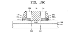
- FIG. 15C is a sectional view taken along line 15C -15C' of FIG. 15B.
- the three corners of the first floating gate 122 are surrounded by the word line 170 and separated from the word line 170 by the first interpoly tunneling insulating layer 164a
- the three corners of the second floating gate 124 are surrounded by the word line 170 and separated from the word line 170 by the second interpoly tunneling insulating layer 164b.
- the second floating gate 124 has the same structure as the first floating gate 122 shown in FIG. 15C.
- a silicon nitride layer is deposited on the entire surface of the resultant structure where the word line 170 is formed, and etched back to form nitride spacers 172 covering the word line 170.
- the third oxide layer 160 which covers the top surface of the silicon island 104, is removed due to over-etching.
- the top surface of the silicon island 104 is exposed adjacent to the nitride spacers 172.
- impurity ions are implanted into the exposed top surface of the silicon island 104 by a typical ion implantation process to form a drain 148 in the silicon island 104.
- impurity ions of the second conductivity type that is opposite to the first conductivity type e.g., n-type impurity ions are implanted at a high concentration.
- the impurity ions are implanted into the drain 148 at a higher concentration than that of the impurity ions for the channel ion implantation.
- Metal silicide layers 159, 179, and 149 are formed on the source line 150, the word line 170, and the drain 148 by using typical salicide process, CVD process, or PVD process.
- the metal silicide layers 159, 179, and 149 can reduce sheet resistance and contact resistance at each contact.
- the source line 150 and the word line 170 are formed of doped polysilicon
- a metal layer is deposited by sputtering on the entire surface of the resultant structure where the drain 148 is formed, and then a primary thermal treatment is performed to form a metal silicide layer of a first phase.
- the metal silicide layers 159, 179, and 149 may be formed of, for example, cobalt silicide, nickel silicide, titanium silicide, hafnium silicide, platinum silicide, or tungsten silicide.
- An insulating material is deposited on the entire surface of the resultant structure where the metal silicide layers 159, 179, and 149 are formed, to form an interlayer dielectric (ILD) 180.
- ILD interlayer dielectric
- a portion of the ILD 180 is etched by a photolithography process to form a contact hole, which exposes the drain 148 of each memory cell.
- a fourth conductive layer is formed on the ILD 180 to a sufficient thickness enough to fill the contact hole, and then patterned by a photolithography process to form a bit line 190.
- the fourth conductive layer may be formed of doped polysilicon or metal. To form the fourth conductive layer using doped polysilicon, an undoped polysilicon layer may be deposited first and then doped, or an already doped polysilicon layer may be deposited.
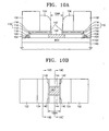
- FIG. 16B is a partial sectional view taken along line 16B - 16B' of FIG. 16A.
- a first floating gate and a second floating gate face each other with the silicon island 104 therebetween, and the first and second floating gates are electrically insulated from each other.
- the first coupling gate insulating layer and the second coupling gate insulating layer, each of which is formed of the second oxide layer 118, are interposed between the channel region of the silicon island 104 and the first floating gate 122 and between the channel region of the silicon island 104 and the second floating gate 124, respectively.
- the word line 170 extends adjacent to the first floating gate 122 and the second floating gate 124.
- the first interpoly tunneling insulating layer 164a is interposed between the first floating gate 122 and the word line 170
- the second interpoly tunneling insulating layer 164b is interposed between the second floating gate 124 and the word line 170.
- two channels 200 are formed along both sidewalls of the silicon island 104 perpendicular to a main surface of the SOI substrate and adjacent to the first coupling gate insulating layer and the second coupling gate insulating layer (each of which is formed of the first oxide layer 118). That is, a non-planar nonvolatile semiconductor memory device, in which the two channels 200 are formed perpendicular to the main surface of the SOI substrate, is provided.
- the nonvolatile semiconductor memory device of embodiments of the present invention is a non-planar split-gate-type device disposed on the SOI substrate.
- Each memory cell includes two floating gates, which face each other with the active region, i.e., the silicon island disposed therebetween . Accordingly, each floating gate has at least three corners, which are adjacent to a control gate and on which an electric field concentrates. In other words, since each memory cell includes a total of six or more corners of the floating gates adjacent to the control gate, the areas of the floating gates, where the electric field concentrates, increase.
- the device of embodiments of the present invention comprises a double-floating gate structure. Both sidewalls of the active region serve as channels such that the channels are formed perpendicular to the main surface of the substrate. This improves the integration density as compared with conventional devices. Also, since the effective channel width for each memory cell can increase in a given layout, a large current can be held in the memory cell.
- the device of embodiments of the present invention has a full depletion mode SOI structure, thus improving a sub-threshold characteristic.
- the non-planar structure including double floating gates, is provided such that a gate is easily controlled so as to suppress the SCE and improve drain induced barrier lowering (DIBL).
- DIBL drain induced barrier lowering
- the SOI structure allows complete isolation between devices and excellent radiation hardness, thus reducing soft errors.
Landscapes
- Non-Volatile Memory (AREA)
- Semiconductor Memories (AREA)
- Thin Film Transistor (AREA)
Applications Claiming Priority (2)
| Application Number | Priority Date | Filing Date | Title |
|---|---|---|---|
| KR2003054782 | 2003-08-07 | ||
| KR10-2003-0054782A KR100518588B1 (ko) | 2003-08-07 | 2003-08-07 | 더블 플로팅 게이트 구조를 가지는 스플릿 게이트형비휘발성 반도체 메모리 소자 및 그 제조 방법 |
Publications (2)
| Publication Number | Publication Date |
|---|---|
| EP1505658A2 true EP1505658A2 (fr) | 2005-02-09 |
| EP1505658A3 EP1505658A3 (fr) | 2005-05-25 |
Family
ID=33550332
Family Applications (1)
| Application Number | Title | Priority Date | Filing Date |
|---|---|---|---|
| EP04254761A Withdrawn EP1505658A3 (fr) | 2003-08-07 | 2004-08-06 | Dispositif semi-conducteur de mémoire rémanente ayant une structure à double grille flottante et procédé pour sa fabrication |
Country Status (6)
| Country | Link |
|---|---|
| US (2) | US7288810B2 (fr) |
| EP (1) | EP1505658A3 (fr) |
| JP (1) | JP2005057296A (fr) |
| KR (1) | KR100518588B1 (fr) |
| CN (1) | CN100470809C (fr) |
| TW (1) | TWI253718B (fr) |
Cited By (1)
| Publication number | Priority date | Publication date | Assignee | Title |
|---|---|---|---|---|
| EP1870941A1 (fr) * | 2006-06-23 | 2007-12-26 | Samsung Electronics Co., Ltd. | Dispositif de mémoire non volatile comportant quatre films de noeuds de stockage et ses procédés de fonctionnement et de fabrication |
Families Citing this family (19)
| Publication number | Priority date | Publication date | Assignee | Title |
|---|---|---|---|---|
| KR100585111B1 (ko) * | 2003-11-24 | 2006-06-01 | 삼성전자주식회사 | 게르마늄 채널 영역을 가지는 비평면 트랜지스터 및 그제조 방법 |
| US7087952B2 (en) * | 2004-11-01 | 2006-08-08 | International Business Machines Corporation | Dual function FinFET, finmemory and method of manufacture |
| JP4761946B2 (ja) * | 2005-11-22 | 2011-08-31 | 株式会社東芝 | 不揮発性半導体記憶素子及びその製造方法並びに不揮発性半導体記憶素子を含む半導体集積回路装置 |
| JP4791868B2 (ja) * | 2006-03-28 | 2011-10-12 | 株式会社東芝 | Fin−NAND型フラッシュメモリ |
| KR100719379B1 (ko) * | 2006-03-30 | 2007-05-17 | 삼성전자주식회사 | 비휘발성 메모리 장치 |
| US7829447B2 (en) * | 2006-05-19 | 2010-11-09 | Freescale Semiconductor, Inc. | Semiconductor structure pattern formation |
| JP4250649B2 (ja) * | 2006-09-26 | 2009-04-08 | 株式会社東芝 | 不揮発性半導体記憶素子及び不揮発性半導体記憶装置 |
| JP4760689B2 (ja) * | 2006-11-30 | 2011-08-31 | セイコーエプソン株式会社 | 半導体装置の製造方法 |
| JP2008205185A (ja) * | 2007-02-20 | 2008-09-04 | Oki Electric Ind Co Ltd | 半導体記憶装置の製造方法、及び半導体記憶装置 |
| CN101442075B (zh) * | 2007-11-21 | 2011-03-16 | 南亚科技股份有限公司 | 闪存 |
| JP2009164349A (ja) * | 2008-01-07 | 2009-07-23 | Toshiba Corp | 不揮発性半導体記憶装置及びその製造方法 |
| CN101901813B (zh) * | 2010-07-20 | 2012-08-01 | 复旦大学 | 一种垂直结构的半导体存储器及其制造方法 |
| US8513728B2 (en) * | 2011-11-17 | 2013-08-20 | Silicon Storage Technology, Inc. | Array of split gate non-volatile floating gate memory cells having improved strapping of the coupling gates |
| CN103426885A (zh) * | 2012-05-22 | 2013-12-04 | 亿而得微电子股份有限公司 | 非自我对准的非挥发性存储器结构 |
| CN104952715B (zh) * | 2014-03-25 | 2018-02-16 | 中芯国际集成电路制造(上海)有限公司 | 半导体结构的形成方法 |
| US9614088B2 (en) * | 2014-08-20 | 2017-04-04 | Taiwan Semiconductor Manufacturing Company Ltd. | Metal gate structure and manufacturing method thereof |
| US9634018B2 (en) * | 2015-03-17 | 2017-04-25 | Silicon Storage Technology, Inc. | Split gate non-volatile memory cell with 3D finFET structure, and method of making same |
| CN107305892B (zh) * | 2016-04-20 | 2020-10-02 | 硅存储技术公司 | 使用两个多晶硅沉积步骤来形成三栅极非易失性闪存单元对的方法 |
| US11476271B2 (en) * | 2020-11-04 | 2022-10-18 | Macronix International Co., Ltd. | Memory device and manufacturing method thereof |
Family Cites Families (17)
| Publication number | Priority date | Publication date | Assignee | Title |
|---|---|---|---|---|
| JPS5718769Y2 (fr) * | 1975-12-31 | 1982-04-20 | ||
| US4380057A (en) * | 1980-10-27 | 1983-04-12 | International Business Machines Corporation | Electrically alterable double dense memory |
| JPS60148168A (ja) * | 1984-01-13 | 1985-08-05 | Seiko Instr & Electronics Ltd | 半導体不揮発性メモリ |
| JPH03126266A (ja) * | 1989-10-12 | 1991-05-29 | Sony Corp | 半導体不揮発性メモリ |
| US5045488A (en) * | 1990-01-22 | 1991-09-03 | Silicon Storage Technology, Inc. | Method of manufacturing a single transistor non-volatile, electrically alterable semiconductor memory device |
| JP3219307B2 (ja) * | 1991-08-28 | 2001-10-15 | シャープ株式会社 | 半導体装置の構造および製造方法 |
| JPH0745797A (ja) * | 1993-07-30 | 1995-02-14 | Toshiba Corp | 半導体記憶装置 |
| JP2870478B2 (ja) * | 1996-04-25 | 1999-03-17 | 日本電気株式会社 | 不揮発性半導体記憶装置及びその動作方法 |
| JP2877103B2 (ja) * | 1996-10-21 | 1999-03-31 | 日本電気株式会社 | 不揮発性半導体記憶装置およびその製造方法 |
| JP4384739B2 (ja) * | 1997-04-04 | 2009-12-16 | 聯華電子股▲ふん▼有限公司 | 半導体装置及びその製造方法 |
| US5973356A (en) * | 1997-07-08 | 1999-10-26 | Micron Technology, Inc. | Ultra high density flash memory |
| JPH11220112A (ja) * | 1998-01-30 | 1999-08-10 | Mitsubishi Electric Corp | 半導体装置およびその製造方法 |
| US6329685B1 (en) * | 1999-09-22 | 2001-12-11 | Silicon Storage Technology, Inc. | Self aligned method of forming a semiconductor memory array of floating gate memory cells and a memory array made thereby |
| KR100368594B1 (ko) * | 2001-02-23 | 2003-01-24 | 삼성전자 주식회사 | 스플릿 게이트형 플래쉬 메모리소자 |
| US6744094B2 (en) * | 2001-08-24 | 2004-06-01 | Micron Technology Inc. | Floating gate transistor with horizontal gate layers stacked next to vertical body |
| KR100431489B1 (ko) * | 2001-09-04 | 2004-05-12 | 한국과학기술원 | 플래쉬 메모리 소자 및 제조방법 |
| US6657252B2 (en) * | 2002-03-19 | 2003-12-02 | International Business Machines Corporation | FinFET CMOS with NVRAM capability |
-
2003
- 2003-08-07 KR KR10-2003-0054782A patent/KR100518588B1/ko not_active Expired - Fee Related
-
2004
- 2004-08-03 TW TW093123182A patent/TWI253718B/zh not_active IP Right Cessation
- 2004-08-06 JP JP2004231612A patent/JP2005057296A/ja active Pending
- 2004-08-06 EP EP04254761A patent/EP1505658A3/fr not_active Withdrawn
- 2004-08-09 US US10/913,489 patent/US7288810B2/en not_active Expired - Lifetime
- 2004-08-09 CN CNB2004100951130A patent/CN100470809C/zh not_active Expired - Fee Related
-
2007
- 2007-09-14 US US11/898,705 patent/US20080006870A1/en not_active Abandoned
Cited By (1)
| Publication number | Priority date | Publication date | Assignee | Title |
|---|---|---|---|---|
| EP1870941A1 (fr) * | 2006-06-23 | 2007-12-26 | Samsung Electronics Co., Ltd. | Dispositif de mémoire non volatile comportant quatre films de noeuds de stockage et ses procédés de fonctionnement et de fabrication |
Also Published As
| Publication number | Publication date |
|---|---|
| JP2005057296A (ja) | 2005-03-03 |
| US20080006870A1 (en) | 2008-01-10 |
| TWI253718B (en) | 2006-04-21 |
| CN100470809C (zh) | 2009-03-18 |
| US7288810B2 (en) | 2007-10-30 |
| TW200527610A (en) | 2005-08-16 |
| EP1505658A3 (fr) | 2005-05-25 |
| KR100518588B1 (ko) | 2005-10-04 |
| KR20050015814A (ko) | 2005-02-21 |
| US20050063215A1 (en) | 2005-03-24 |
| CN1607669A (zh) | 2005-04-20 |
Similar Documents
| Publication | Publication Date | Title |
|---|---|---|
| US20080006870A1 (en) | Nonvolatile semiconductor memory device having double floating gate structure and method of manufacturing the same | |
| CN101051652B (zh) | 半导体器件及其制造方法 | |
| JP4116428B2 (ja) | マルチビットメモリセルを作製する方法 | |
| EP1227518B1 (fr) | Procédé de fabrication de dispositif de circuit intégré à semi-conducteur comprenant des dispositifs de mémoire à semi-conducteur non-volatiles | |
| US6750525B2 (en) | Non-volatile memory device having a metal-oxide-nitride-oxide-semiconductor gate structure | |
| US6809385B2 (en) | Semiconductor integrated circuit device including nonvolatile semiconductor memory devices having control gates connected to common contact section | |
| US20080111180A1 (en) | Split gate flash memory device having self-aligned control gate and method of manufacturing the same | |
| US20050184330A1 (en) | Nonvolatile memories and methods of fabrication | |
| US7799635B2 (en) | Methods of forming nonvolatile memory devices | |
| US7256448B2 (en) | Split gate type nonvolatile semiconductor memory device, and method of fabricating the same | |
| US6337245B1 (en) | Method for fabricating flash memory device and flash memory device fabricated thereby | |
| US7183157B2 (en) | Nonvolatile memory devices | |
| JP3544308B2 (ja) | 不揮発性半導体記憶装置の製造方法 | |
| US7408230B2 (en) | EEPROM device having first and second doped regions that increase an effective channel length | |
| US20070128799A1 (en) | Method of fabricating flash memory | |
| US20040185616A1 (en) | Nonvolatile memories and methods of fabrication | |
| KR100351051B1 (ko) | 이층 구조의 플로팅 게이트를 갖는 불휘발성 메모리 셀의 제조 방법 | |
| US7019354B2 (en) | Electrically erasable programmable read only memory (EEPROM) cells and methods of fabricating the same | |
| US20080157163A1 (en) | EEPROM device and method of forming the same | |
| KR100683389B1 (ko) | 플래시 메모리의 셀 트랜지스터 및 그 제조 방법 | |
| KR100703981B1 (ko) | 비휘발성 메모리 소자 및 그 제조 방법 | |
| CN121843124A (zh) | 用于制造半导体装置的方法 | |
| WO2006064394A1 (fr) | Empilement de couche sans bord (a gravure) pour applications a memoire non volatile |
Legal Events
| Date | Code | Title | Description |
|---|---|---|---|
| PUAI | Public reference made under article 153(3) epc to a published international application that has entered the european phase |
Free format text: ORIGINAL CODE: 0009012 |
|
| 17P | Request for examination filed |
Effective date: 20040818 |
|
| AK | Designated contracting states |
Kind code of ref document: A2 Designated state(s): AT BE BG CH CY CZ DE DK EE ES FI FR GB GR HU IE IT LI LU MC NL PL PT RO SE SI SK TR |
|
| AX | Request for extension of the european patent |
Extension state: AL HR LT LV MK |
|
| PUAL | Search report despatched |
Free format text: ORIGINAL CODE: 0009013 |
|
| AK | Designated contracting states |
Kind code of ref document: A3 Designated state(s): AT BE BG CH CY CZ DE DK EE ES FI FR GB GR HU IE IT LI LU MC NL PL PT RO SE SI SK TR |
|
| AX | Request for extension of the european patent |
Extension state: AL HR LT LV MK |
|
| AKX | Designation fees paid |
Designated state(s): DE FR GB NL |
|
| 17Q | First examination report despatched |
Effective date: 20060224 |
|
| GRAP | Despatch of communication of intention to grant a patent |
Free format text: ORIGINAL CODE: EPIDOSNIGR1 |
|
| RIC1 | Information provided on ipc code assigned before grant |
Ipc: H01L 21/336 20060101ALN20091006BHEP Ipc: H01L 21/8247 20060101ALN20091006BHEP Ipc: H01L 27/115 20060101ALI20091006BHEP Ipc: H01L 29/788 20060101AFI20091006BHEP |
|
| STAA | Information on the status of an ep patent application or granted ep patent |
Free format text: STATUS: THE APPLICATION IS DEEMED TO BE WITHDRAWN |
|
| 18D | Application deemed to be withdrawn |
Effective date: 20100303 |