EP1505659A1 - Leistungsquelleneinrichtung - Google Patents
Leistungsquelleneinrichtung Download PDFInfo
- Publication number
- EP1505659A1 EP1505659A1 EP03721100A EP03721100A EP1505659A1 EP 1505659 A1 EP1505659 A1 EP 1505659A1 EP 03721100 A EP03721100 A EP 03721100A EP 03721100 A EP03721100 A EP 03721100A EP 1505659 A1 EP1505659 A1 EP 1505659A1
- Authority
- EP
- European Patent Office
- Prior art keywords
- output
- cells
- light
- outputs
- voltage
- Prior art date
- Legal status (The legal status is an assumption and is not a legal conclusion. Google has not performed a legal analysis and makes no representation as to the accuracy of the status listed.)
- Withdrawn
Links
Images




Classifications
-
- H—ELECTRICITY
- H02—GENERATION; CONVERSION OR DISTRIBUTION OF ELECTRIC POWER
- H02S—GENERATION OF ELECTRIC POWER BY CONVERSION OF INFRARED RADIATION, VISIBLE LIGHT OR ULTRAVIOLET LIGHT, e.g. USING PHOTOVOLTAIC [PV] MODULES
- H02S10/00—PV power plants; Combinations of PV energy systems with other systems for the generation of electric power
-
- H—ELECTRICITY
- H02—GENERATION; CONVERSION OR DISTRIBUTION OF ELECTRIC POWER
- H02J—ELECTRIC POWER NETWORKS; CIRCUIT ARRANGEMENTS OR SYSTEMS FOR SUPPLYING OR DISTRIBUTING ELECTRIC POWER; SYSTEMS FOR STORING ELECTRIC ENERGY
- H02J7/00—Circuit arrangements for charging or discharging batteries or for supplying loads from batteries
- H02J7/34—Parallel operation in networks using both storage and other DC sources, e.g. providing buffering
- H02J7/35—Parallel operation in networks using both storage and other DC sources, e.g. providing buffering with light sensitive cells
-
- H—ELECTRICITY
- H01—ELECTRIC ELEMENTS
- H01G—CAPACITORS; CAPACITORS, RECTIFIERS, DETECTORS, SWITCHING DEVICES, LIGHT-SENSITIVE OR TEMPERATURE-SENSITIVE DEVICES OF THE ELECTROLYTIC TYPE
- H01G9/00—Electrolytic capacitors, rectifiers, detectors, switching devices, light-sensitive or temperature-sensitive devices; Processes of their manufacture
- H01G9/20—Light-sensitive devices
- H01G9/2027—Light-sensitive devices comprising an oxide semiconductor electrode
- H01G9/2031—Light-sensitive devices comprising an oxide semiconductor electrode comprising titanium oxide, e.g. TiO2
-
- H—ELECTRICITY
- H01—ELECTRIC ELEMENTS
- H01G—CAPACITORS; CAPACITORS, RECTIFIERS, DETECTORS, SWITCHING DEVICES, LIGHT-SENSITIVE OR TEMPERATURE-SENSITIVE DEVICES OF THE ELECTROLYTIC TYPE
- H01G9/00—Electrolytic capacitors, rectifiers, detectors, switching devices, light-sensitive or temperature-sensitive devices; Processes of their manufacture
- H01G9/20—Light-sensitive devices
- H01G9/2068—Panels or arrays of photoelectrochemical cells, e.g. photovoltaic modules based on photoelectrochemical cells
-
- H—ELECTRICITY
- H01—ELECTRIC ELEMENTS
- H01G—CAPACITORS; CAPACITORS, RECTIFIERS, DETECTORS, SWITCHING DEVICES, LIGHT-SENSITIVE OR TEMPERATURE-SENSITIVE DEVICES OF THE ELECTROLYTIC TYPE
- H01G9/00—Electrolytic capacitors, rectifiers, detectors, switching devices, light-sensitive or temperature-sensitive devices; Processes of their manufacture
- H01G9/20—Light-sensitive devices
- H01G9/2068—Panels or arrays of photoelectrochemical cells, e.g. photovoltaic modules based on photoelectrochemical cells
- H01G9/2072—Panels or arrays of photoelectrochemical cells, e.g. photovoltaic modules based on photoelectrochemical cells comprising two or more photoelectrodes sensible to different parts of the solar spectrum, e.g. tandem cells
-
- H—ELECTRICITY
- H01—ELECTRIC ELEMENTS
- H01G—CAPACITORS; CAPACITORS, RECTIFIERS, DETECTORS, SWITCHING DEVICES, LIGHT-SENSITIVE OR TEMPERATURE-SENSITIVE DEVICES OF THE ELECTROLYTIC TYPE
- H01G9/00—Electrolytic capacitors, rectifiers, detectors, switching devices, light-sensitive or temperature-sensitive devices; Processes of their manufacture
- H01G9/20—Light-sensitive devices
- H01G9/2059—Light-sensitive devices comprising an organic dye as the active light absorbing material, e.g. adsorbed on an electrode or dissolved in solution
- H01G9/2063—Light-sensitive devices comprising an organic dye as the active light absorbing material, e.g. adsorbed on an electrode or dissolved in solution comprising a mixture of two or more dyes
-
- Y—GENERAL TAGGING OF NEW TECHNOLOGICAL DEVELOPMENTS; GENERAL TAGGING OF CROSS-SECTIONAL TECHNOLOGIES SPANNING OVER SEVERAL SECTIONS OF THE IPC; TECHNICAL SUBJECTS COVERED BY FORMER USPC CROSS-REFERENCE ART COLLECTIONS [XRACs] AND DIGESTS
- Y02—TECHNOLOGIES OR APPLICATIONS FOR MITIGATION OR ADAPTATION AGAINST CLIMATE CHANGE
- Y02E—REDUCTION OF GREENHOUSE GAS [GHG] EMISSIONS, RELATED TO ENERGY GENERATION, TRANSMISSION OR DISTRIBUTION
- Y02E10/00—Energy generation through renewable energy sources
- Y02E10/50—Photovoltaic [PV] energy
- Y02E10/542—Dye sensitized solar cells
Definitions
- the present invention relates to power supply units including cells, for example, solar cells (photoelectric transducers) and chemical cells.
- a solar cell is a type of photoelectric transducer for converting light energy into electrical energy.
- a wet solar cell making use of photoinduced electron transfer is known as a solar cell based on a new principle.
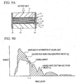
- Fig. 9A is a schematic sectional view of a typical wet solar cell.
- the wet solar cell mainly includes a transparent substrate 11 composed of, e.g., glass, a transparent electrode 12 of, e.g., indium tin oxide (ITO), a semiconductor layer 14 of, e.g., titanium dioxide (TiO 2 ), a counter electrode 17, an electrolyte layer 16 retained between the semiconductor layer 14 and the counter electrode 17, and a substrate 19.
- ITO indium tin oxide
- TiO 2 titanium dioxide
- a light-absorbing member 15 composed of, e.g., ruthenium complex photosensitizing dye is applied to a surface of the semiconductor layer 14 toward the electrolyte layer 16; the light-absorbing member 15 has an absorption spectrum in the visible-light region.
- the device When light enters the device shown in Fig. 9A, the device functions as a cell including the counter electrode 17 as a positive electrode and the transparent electrode 12 as a negative electrode.
- the principle of the cell will now be described.
- the light-absorbing member 15 When the light-absorbing member 15 absorbs photons entering the semiconductor layer 14, electrons in a ground state in the light-absorbing member 15 are excited into an excited state. Since electrical coupling by, for example, a carboxyl group occurs between the light-absorbing member 15 and the semiconductor layer 14, the electrons in an excited state move to the conduction band of the semiconductor layer 14 and reach the transparent electrode 12 through the semiconductor layer 14.
- positive ions generated by the loss of electrons in the light-absorbing member 15 gain electrons from negative ions in the electrolyte layer 16 and are electrically neutralized.
- the negative ions having lost the electrons diffuse into the counter electrode 17 and gain electrons from the counter electrode 17.
- Energy possessed by one photon is proportional to the frequency of light or is inversely proportional to the wavelength of light.
- Ordinary light, for example, solar light includes a wide range of light components having different wavelengths, and thus consists of photons having different energies.
- Electrons in a substance inevitably have only a few energy states inherent in the substance, which are quantum-mechanically determined.
- the energy difference between electrons in a ground state and those in an excited state i.e., the energy required for exciting the electrons in a ground state into an excited state, has a fixed value inherent in the substance.
- this energy is referred to as excitation energy Ex, and the wavelength of a photon having the same energy is denoted as ⁇ x.
- the energy difference between the valence band (ground state) and the conduction band (excited state), i.e., the band-gap energy, is the excitation energy Ex.
- the energy difference between a ground state and an excited state in a light-absorbing member is the excitation energy Ex.
- Fig. 8 is a graph illustrating the rate of light energy converted into electrical energy when light uniformly including all light components having wavelengths around visible light enters a solar cell.
- the light components having wavelengths that are longer than ⁇ x and having photon energies that are less than the excitation energy Ex cannot excite electrons and are not absorbed. Thus, the energies of these light components are not converted into electrical energy. That is, the energies of the light components having wavelengths longer than ⁇ x cannot be used and are thus wasted, as shown in a shaded area (I) of Fig. 8.
- Fig. 9B is a graph illustrating the rate of solar light energy converted into electrical energy by the wet solar cell shown in Fig. 9A.
- the light from the sun to the earth has a wavelength distribution shown in Fig. 9B.
- the maximum energy conversion efficiency does not exceed about 33 percent due to the above trade-off relationship.
- Tandem solar cells including a plurality of photoelectric transducers having different light-absorbing wavelength characteristics, i.e., different Ex values, have been proposed to overcome the above trade-off relationship for achieving a higher energy conversion efficiency.
- the photoelectric transducers are stacked along the transmission direction of light.
- tandem solar cells are disclosed in, for example, Japanese Unexamined Patent Application Publication Nos. 11-273753, 2000-90989, and 2000-100483.
- each of the photoelectric transducers stacked in a tandem solar cell is referred to as a tandem photoelectric transducer.
- tandem solar cell In the tandem solar cell, light components having certain wavelengths that cannot be absorbed by a tandem photoelectric transducer at the previous stage can be absorbed by a tandem photoelectric transducer at the next stage. Thus, light absorption efficiency can be improved, resulting in a higher energy conversion efficiency.
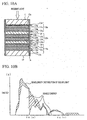
- Fig. 10A is a schematic sectional view of a typical tandem wet solar cell 10. Tandem photoelectric transducers 10a, 10b, and 10c are stacked in this order from the position closest to the incident light.
- Each tandem photoelectric transducer has substantially the same structure as the single-layered wet solar cell shown in Fig. 9A.
- the tandem photoelectric transducer 10a includes, for example, a glass substrate 11, a transparent electrode 12a, a semiconductor layer 14a, a light-absorbing member 15a, an electrolyte layer 16a, a counter electrode 17a, and a spacer 20 corresponding to the substrate 19.
- the counter electrode 17a, the spacer 20, and the like are composed of transparent materials and have structures that easily transmit light so that light components that are not absorbed by the light-absorbing member 15a can pass through to the next tandem photoelectric transducer.
- the absorption wavelengths of the light-absorbing members 15a to 15c are preferably different from each other.
- an anthraquinone yellow dye is used as the light-absorbing member 15a
- an anthraquinone magenta dye is used as the light-absorbing member 15b
- an anthraquinone cyan dye is used as the light-absorbing member 15c.
- the semiconductor layers 14a to 14c are preferably optimized according to the light-absorbing members 15a to 15c so that excitation energy absorbed by electrons in the light-absorbing members is effectively utilized as much as possible, and conserved as electron energy in conduction bands of the semiconductor layers, the conserved energy being output as an electromotive force of a cell. That is, each of the light-absorbing members 15a to 15c is matched with a semiconductor having a band-gap energy that is as close as possible to the excitation energy of each of the light-absorbing members.
- a light-absorbing member that absorbs light components having short wavelengths and has large excitation energy is matched with zirconium dioxide (ZrO 2 ) in place of titanium dioxide (TiO 2 ).
- ZrO 2 zirconium dioxide
- TiO 2 titanium dioxide
- a light-absorbing member that absorbs light components having long wavelengths and has small excitation energy is matched with tin dioxide (SnO 2 ).
- Fig. 10B is a graph illustrating the rate of solar light energy converted into electrical energy by the tandem solar cell having the above structure.
- Fig. 10B shows that a tandem solar cell utilizes long wavelength components of solar light, which are not utilized by a single-layered solar cell, and improves the energy conversion efficiency of short wavelength components.
- This arrangement is set up so that the output currents from the transducers are equal to each other for a standard wavelength distribution of solar light.
- the wavelength distribution of solar light deviates from the standard one in, for example, the summer and the winter seasons, and during the daytime, the morning, and the evening, the output currents from the stacked transducers are greatly different from each other.
- any transducers outputting a low current due to a low level of light increases the internal resistance of the overall cell.
- the output currents are disadvantageously restricted.
- Another problem is that the pattern used for assigning a wavelength range to each of the tandem photoelectric transducers for equalizing the output currents from the transducers does not generally agree with that used for assigning a wavelength range to each transducer for utilizing solar light at the maximum efficiency.
- the series connection restricts the assignment of light-absorbing wavelength characteristic to each transducer, and prevents the solar light from being used at its maximum efficiency, which is a problem.
- the present invention is intended to address the above problems. It is an object of the present invention to provide a power supply unit composed so that outputs from a plurality of cells having different output characteristic's are output from common terminals and so that a decrease in energy efficiency caused by connecting the cells is suppressed to the utmost.
- the present invention relates to a power supply unit including a plurality of cells having different output characteristics and being disposed in parallel. Outputs of the plurality of cells are adjusted to have the same voltage, and the outputs are output from common terminals.
- the outputs of the plurality of cells having different output voltages and output currents, are adjusted to have the same output voltage value, the outputs are then output to the common terminals so as to match the parallel connection.
- a plurality of cells are preferably connected in parallel to each other through respective voltage-regulating circuits.
- the outputs from a plurality of cells may be stored in respective capacitors, and the stored charge in each capacitor may be output by time-sharing as a uniform voltage through a single voltage-regulating circuit that can connect to each capacitor.
- each of a plurality of cells may include units and the number of units connected to each other in series in each of rows and the number of the rows connected to each other in parallel are adjustable.
- these cells may be photoelectric transducers, e.g., solar cells, which are stacked along the transmission direction of light and have different optical absorption properties.
- Fig. 1 is a schematic block diagram illustrating a power supply unit in which outputs of tandem photoelectric transducers 10a to 10c in a tandem wet solar cell 10 are connected in parallel to common output terminals 1 and 2 through voltage-regulating circuits 3a to 3c.
- Fig. 10A is a schematic sectional view of the tandem wet solar cell 10.
- the tandem photoelectric transducers 10a, 10b, and 10c are respectively retained in a first layer, a second layer; and a third layer, these layers being formed by a transparent substrate 11, two spacers 20, and another substrate 19.
- the spacers 20 are composed of a transparent material and have a shape allowing light to pass through.
- the spacers 20 may be, for example, transparent glass plates or transparent plastic plates composed of, e.g., polyethylene terephthalate or polycarbonate. Since the substrate 19 is not required to transmit light, a nontransparent glass plate, plastic plate, ceramic plate, or metal plate may be used as the substrate 19.
- the tandem photoelectric transducers 10a to 10c have the same structure. These transducers, respectively, include transparent electrodes 12a to 12c and counter electrodes 17a to 17c composed of, for example, indium tin oxide (ITO); semiconductor layers 14a to 14c composed of, for example, titanium dioxide (TiO 2 ); light-absorbing members 15a to 15c; electrolyte layers 16a to 16c; and the like.
- transparent electrodes 12a to 12c and counter electrodes 17a to 17c composed of, for example, indium tin oxide (ITO); semiconductor layers 14a to 14c composed of, for example, titanium dioxide (TiO 2 ); light-absorbing members 15a to 15c; electrolyte layers 16a to 16c; and the like.
- ITO indium tin oxide
- semiconductor layers 14a to 14c composed of, for example, titanium dioxide (TiO 2 )
- light-absorbing members 15a to 15c electrolyte layers 16a to 16c; and the like.
- the electrolyte layers 16a to 16c may be composed of an electrolyte solution, or a gelled or solid electrolyte.
- the electrolyte solution may be composed of, for example, a solution containing an iodide/triiodide (I-/I 3 -) oxidation-reduction system or redox couple. Specifically, a solution containing iodine and ammonium iodide dissolved in a solvent of, for example, acetonitrile is used. Side faces of the cell are sealed with encapsulants 18 of, for example, epoxy thermosetting resin, acrylic UV curable resin, or liquid glass.
- the absorption wavelengths of the light-absorbing members 15a to 15c are different from each other.
- an anthraquinone yellow dye is used as the light-absorbing member 15a
- an anthraquinone magenta dye is used as the light-absorbing member 15b
- an anthraquinone cyan dye is used as the light-absorbing member 15c.
- the voltage-regulating circuits 3a to 3c may be of a voltage step-up type, a voltage step-down type, or a voltage step-up/step-down type. A type exhibiting low power-consumption and high efficiency is preferable.
- the voltage-regulating circuits may be a known DC-DC converter.
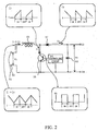
- Fig. 2 shows a typical step-ug chopper-type constant-voltage circuit.
- An output voltage V I from the tandem photoelectric transducers is input to an input terminal 51 and a grounding terminal 52, and an output voltage V 0 that is stepped up to have a desired voltage value is output across an output terminal 53 and a grounding terminal 54.
- a coil 55 and a switching transistor 56 are interposed in series between the input terminal 51 and the grounding terminal 52.
- a current I 1 flows and energy is stored in the coil 55.
- the coil 55, a diode 57, and a capacitor 58 are interposed in series between the input terminal 51 and the grounding terminal 52.
- a current I 2 that is stepped up by a back electromotive force of the coil 55 flows through the diode 57 to charge the capacitor 58.
- output energy from the tandem photoelectric transducers, which is stored in the coil 55 is output to an output side as energy charged in the capacitor 58.
- control pulses having a rectangular waveform are applied to the base terminal of the switching transistor 56 from a controlling circuit 59.
- the current I 1 starts to flow through the coil 55 and the transistor 56 from the tandem photoelectric transducers.
- the output voltage V I can be assumed to be constant for at least several cycles.
- I 1E I 1S + (V I /L)t ON
- I 2E I 2S - (V 0 - V I )t OFF /L
- I 2E e.g., the value of I 2 at the end of the period for which the transistor 56 is turned off is equal to the above-described I 1S
- I 2S e.g., the value of I 2 at the beginning of the period for which the transistor 56 is turned off is equal to the above-described I 1E .
- the equation V 0 (t ON + t OFF )V I /t OFF is obtained by re-arranging the above equations.
- the output voltage V 0 can be kept constant by adjusting t ON /t OFF .
- the controlling circuit 59 keeps the output voltage V 0 constant by monitoring the output voltage V 0 and by increasing or decreasing the duty ratio of pulses having a rectangular waveform according to deviation of the voltage from a predetermined value.
- tandem photoelectric transducers need be provided with the voltage-regulating circuits.
- One tandem photoelectric transducer may be designated as a reference transducer, and the other tandem photoelectric transducers may be provided with the voltage-regulating circuits.
- the output currents from the tandem photoelectric transducers are output so as to match the parallel connection, the output currents from the transducers are not required to be the same as each other, unlike the series connection.
- a light-absorbing wavelength characteristic can be assigned to each tandem photoelectric transducer so that solar light is utilized at the maximum efficiency.
- Fig. 3 is a schematic block diagram illustrating a power supply unit that stores energies generated by tandem photoelectric transducers 10a, 10b, and 10c, respectively, of a tandem wet solar cell 10 in capacitors 4a, 4b, and 4c as electric charge.
- the power supply unit then outputs the energies stored in the capacitors by time-sharing as currents at the same voltage across common output terminals 1 and 2 through a voltage-regulating circuit 3d that can connect to the capacitors.
- This output technique using switched capacitors is a modification of the output technique in the first embodiment, Since outputs of the tandem photoelectric transducers 10a to 10c are not simultaneously connected to the common output terminal 1 after the voltages are adjusted, these outputs are not connected to each other in parallel in the strict sense. However, this output technique matches the parallel connection in that all the tandem photoelectric transducers 10a to 10c are substantially connected in parallel to the common output terminal 1. Thus, this output technique can be regarded as a modification of the parallel connection.
- first and second embodiments are as follows:
- first embodiment as many voltage-regulating circuits 3a to 3c as the tandem photoelectric transducers are provided to constantly adjust the voltage of the output of each tandem photoelectric transducer, whereas, in the second embodiment, the functions of a plurality of voltage-regulating circuits are integrated into one voltage-regulating circuit 3d, which adjusts the voltage of the output of each tandem photoelectric transducer by time-sharing.
- the capacitors 4a, 4b, and 4c in the second embodiment are attached to temporarily store the outputs of the tandem photoelectric transducers 10a, 10b, and 10c, respectively, for a wait time required for processing.
- a voltage-regulating circuit similar to that used in the first embodiment can used as the voltage-regulating circuit 3d on condition that the circuit provides a quick response because processing is required to be completed in a limited time.
- a known multiplexer including a semiconductor switch is preferably used as a device for switching inputs of the voltage-regulating circuit 3d.
- applicable devices are not in principle limited to the multiplexer.
- a mechanical switch which switches contact points may be used.
- the second embodiment is identical to the first embodiment in that the outputs of the tandem photoelectric transducers are output to the common terminals so as to match the parallel connection.
- the outputs of the tandem photoelectric transducers are output to the common terminals so as to match the parallel connection.
- Fig. 4 is a schematic block diagram illustrating a power supply unit according to a third embodiment.
- the power supply unit includes tandem photoelectric transducers 10a to 10c in respective photoelectric layers, each transducer including many small cells having the same size.
- the power supply unit produces the same output voltages in all the layers only by setting connections among the small cells in each layer and outputs these voltages in parallel across the common output terminals 1 and 2.
- This embodiment does not need a voltage-regulating circuit such as a voltage step-up/step-down circuit, unlike the first and second embodiments.
- Double connecting lines in Fig. 4 indicate that the small cells are connected in a matrix by both the series and the parallel connections.
- a number of rows, each including a predetermined number of small cells connected in series are connected to each other in parallel.
- the small cells connected in a matrix are called a cell matrix as a whole.
- the output voltage of each matrix is the product of the electromotive force of each layer and the number of small cells connected in series in each layer. To equalize the output voltages of the cell matrixes in the layers, the number of small cells connected in series in a row and the total number of small cells that enables this series connection must be determined in consideration of the electromotive force of each layer.
- a first layer has an electromotive force of 0.6 V
- a second layer has an electromotive force of 0.4 V
- a third layer has an electromotive force of 0.3 V.
- the least common multiple of 6, 4, and 3 is 12.
- the common output voltage is fixed at 1.2 V or 1.2n V, where n is an integer.
- each of the tandem photoelectric transducers 10a to 10c in each photoelectric layer must include twelve small cells in advance, twelve being the least common multiple of two, three, and four.
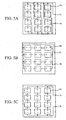
- Fig. 5A is a schematic plan view illustrating the cell matrix, in the first photoelectric layer, including twelve small cells 6a obtained by dividing the tandem photoelectric transducer 10a in the first layer.
- Fig. 5B is a schematic plan view illustrating the cell matrix, in the second photoelectric layer, including twelve small cells 6b obtained by dividing the tandem photoelectric transducer 10b in the second layer.
- Fig. 5C is a schematic plan view illustrating the' cell matrix, in the third photoelectric layer, including twelve small cells 6c obtained by dividing the tandem photoelectric transducer 10c in the third layer.
- Each cell matrix is wired so as to produce the same output voltage of 1.2 V. Outputs of the cell matrixes in the above layers are, respectively, output from paired output terminals 7a and 8a, 7b and 8b, and 7c and 8c.
- Figs. 6 and 7 illustrate examples of the second technique.
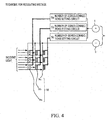
- Fig. 6 illustrates a circuit that changes the number of cells connected in series in a row with a sliding switch having multiple contact points.
- a sliding switch 62 is located at a position represented by the dotted lines, each output produced by three small cells 61 connected in series is output across output terminals 63 and 64.
- each output produced by four small cells connected in series is output across output terminals 65 and 66.
- Fig. 7 illustrates a typical circuit that changes the number of cells connected in series in a row using a gate circuit including transistors.
- the on-off operations of transistors 72 to 76 are respectively controlled by applying control signals to control terminals 72a to 76a.
- the electromotive force of a small cell 81 is output across output terminals 77 and 78.
- the transistors 73 and 75 are conductive, the voltage produced by a series connection of the small cell 81 and a small cell 82 is output across the output terminals 77 and 78.
- the transistors 74, 75, and 76 are conductive and the transistors 72 and 73 are cut off, the voltage produced by a series connection of the small-cells 81 and 82 and a small cell 83 is output across the output terminals 77 and 78.
- the third embodiment is the same as the first and the second embodiments in that the outputs are output to the common terminals so as to match the parallel connection.
- the first or the second embodiments and the third embodiment can be used in combination. That is, outputs adjusted in advance to have a voltage value near a target output voltage value by a plurality of small cells connected in series in a row using the technique of the third embodiment are used as inputs to voltage-regulating circuits according to the first and the second embodiments.
- the present invention can be efficiently applied to not only power supply units including solar cells but power supply units including other cells, such as chemical cells, for example, emergency power supply units including lead-acid cells, and power generating units including fuel cells, for the reasons described below.
- the outputs of a plurality of cells having different output voltages and output currents, are adjusted to have the same output voltage value, the outputs are then output to common terminals so as to match the parallel connection.
- a cell outputting a low current does not restrict the output currents of the overall power supply unit and does not decease the photoelectric energy conversion efficiency.
- a light-absorbing wavelength characteristic can be assigned to each tandem photoelectric transducer so that solar light is utilized at the maximum efficiency.
Landscapes
- Engineering & Computer Science (AREA)
- Power Engineering (AREA)
- Microelectronics & Electronic Packaging (AREA)
- Chemical & Material Sciences (AREA)
- Chemical Kinetics & Catalysis (AREA)
- Electrochemistry (AREA)
- Life Sciences & Earth Sciences (AREA)
- Sustainable Development (AREA)
- Photovoltaic Devices (AREA)
- Charge And Discharge Circuits For Batteries Or The Like (AREA)
- Hybrid Cells (AREA)
Applications Claiming Priority (3)
| Application Number | Priority Date | Filing Date | Title |
|---|---|---|---|
| JP2002138211 | 2002-05-14 | ||
| JP2002138211A JP2003333757A (ja) | 2002-05-14 | 2002-05-14 | 電源装置 |
| PCT/JP2003/005939 WO2003100867A1 (fr) | 2002-05-14 | 2003-05-13 | Bloc d'alimentation |
Publications (1)
| Publication Number | Publication Date |
|---|---|
| EP1505659A1 true EP1505659A1 (de) | 2005-02-09 |
Family
ID=29561170
Family Applications (1)
| Application Number | Title | Priority Date | Filing Date |
|---|---|---|---|
| EP03721100A Withdrawn EP1505659A1 (de) | 2002-05-14 | 2003-05-13 | Leistungsquelleneinrichtung |
Country Status (7)
| Country | Link |
|---|---|
| US (1) | US20050268957A1 (de) |
| EP (1) | EP1505659A1 (de) |
| JP (1) | JP2003333757A (de) |
| KR (1) | KR20050013992A (de) |
| CN (1) | CN1653623A (de) |
| AU (1) | AU2003235234A1 (de) |
| WO (1) | WO2003100867A1 (de) |
Cited By (1)
| Publication number | Priority date | Publication date | Assignee | Title |
|---|---|---|---|---|
| EP3144945A4 (de) * | 2014-05-12 | 2017-05-31 | Sharp Kabushiki Kaisha | Vorrichtung zur lichtenergieerzeugung |
Families Citing this family (51)
| Publication number | Priority date | Publication date | Assignee | Title |
|---|---|---|---|---|
| JP3717506B2 (ja) | 2004-01-20 | 2005-11-16 | シャープ株式会社 | 色素増感型太陽電池モジュール |
| US7812569B2 (en) * | 2004-12-17 | 2010-10-12 | Visteon Global Technologies, Inc. | Circuit to measure vehicle battery voltage |
| US20090242027A1 (en) * | 2006-07-05 | 2009-10-01 | Teruhisa Inoue | Dye-Sensitized Solar Cell |
| KR100842265B1 (ko) * | 2006-11-21 | 2008-06-30 | 한국전자통신연구원 | 수직 적층형 염료감응 태양전지 모듈의 제조 방법 |
| TW200827974A (en) * | 2006-12-18 | 2008-07-01 | Ming-Hsin Sun | Power tracking system of solar energy system and the method thereof |
| US20080216885A1 (en) * | 2007-03-06 | 2008-09-11 | Sergey Frolov | Spectrally adaptive multijunction photovoltaic thin film device and method of producing same |
| JP2008257895A (ja) * | 2007-03-31 | 2008-10-23 | Shinshu Univ | 色素増感太陽電池の製造方法、および色素増感太陽電池 |
| US20080257405A1 (en) * | 2007-04-18 | 2008-10-23 | Emcore Corp. | Multijunction solar cell with strained-balanced quantum well middle cell |
| KR100927721B1 (ko) * | 2007-09-17 | 2009-11-18 | 삼성에스디아이 주식회사 | 광전변환소자 및 이의 제조방법 |
| US9048353B2 (en) | 2008-07-01 | 2015-06-02 | Perfect Galaxy International Limited | Photovoltaic DC/DC micro-converter |
| WO2010002960A1 (en) * | 2008-07-01 | 2010-01-07 | Satcon Technology Corporation | Photovoltaic dc/dc micro-converter |
| MX2011000271A (es) * | 2008-07-09 | 2011-04-05 | Christopher Scott Eiman | Dispositivo de ensombrecimiento personalizado que incluye capacidades fotovoltaicas. |
| JP5376850B2 (ja) * | 2008-07-16 | 2013-12-25 | 国立大学法人京都大学 | 広帯域波長領域の光電変換を可能にする太陽電池 |
| CN102265453B (zh) | 2008-10-29 | 2014-10-01 | 富士胶片株式会社 | 色素、使用其的光电转换元件、光电化学电池、及色素的制造方法 |
| JP2010278405A (ja) * | 2009-06-01 | 2010-12-09 | Smart Solar International Inc | 太陽光発電システム及び太陽光発電装置 |
| JP5582744B2 (ja) * | 2009-08-20 | 2014-09-03 | 日立造船株式会社 | 太陽電池およびその製造方法並びに太陽電池装置 |
| JP5524557B2 (ja) | 2009-09-28 | 2014-06-18 | 富士フイルム株式会社 | 光電変換素子の製造方法、光電変換素子、および光電気化学電池 |
| JP5620081B2 (ja) | 2009-09-28 | 2014-11-05 | 富士フイルム株式会社 | 光電変換素子の製造方法 |
| JP5007772B2 (ja) * | 2010-06-23 | 2012-08-22 | 大日本印刷株式会社 | 有機系太陽電池モジュールおよび有機系太陽電池パネル |
| JP5912404B2 (ja) | 2010-10-29 | 2016-04-27 | 株式会社半導体エネルギー研究所 | 光電変換装置 |
| JP5663740B2 (ja) * | 2010-12-01 | 2015-02-04 | 日本電信電話株式会社 | 太陽光発電装置 |
| US9559235B2 (en) | 2010-12-17 | 2017-01-31 | Semiconductor Energy Laboratory Co., Ltd. | Photoelectric conversion device |
| US9389315B2 (en) | 2012-12-19 | 2016-07-12 | Basf Se | Detector comprising a transversal optical sensor for detecting a transversal position of a light beam from an object and a longitudinal optical sensor sensing a beam cross-section of the light beam in a sensor region |
| CN105210190A (zh) | 2013-06-13 | 2015-12-30 | 巴斯夫欧洲公司 | 光学检测器及其制造方法 |
| US10353049B2 (en) | 2013-06-13 | 2019-07-16 | Basf Se | Detector for optically detecting an orientation of at least one object |
| AU2014280332B2 (en) | 2013-06-13 | 2017-09-07 | Basf Se | Detector for optically detecting at least one object |
| AU2014310703B2 (en) | 2013-08-19 | 2018-09-27 | Basf Se | Optical detector |
| JP6483127B2 (ja) | 2013-08-19 | 2019-03-13 | ビーエーエスエフ ソシエタス・ヨーロピアBasf Se | 少なくとも1つの対象物の位置を求めるための検出器 |
| WO2016005893A1 (en) | 2014-07-08 | 2016-01-14 | Basf Se | Detector for determining a position of at least one object |
| KR102452393B1 (ko) | 2014-09-29 | 2022-10-11 | 바스프 에스이 | 적어도 하나의 물체의 포지션을 광학적으로 결정하기 위한 방법 및 검출기 및 이를 이용한 휴먼 머신 인터페이스, 엔터테인먼트 장치, 추적 시스템, 스캐닝 시스템, 입체 시스템 및 카메라 |
| US11125880B2 (en) | 2014-12-09 | 2021-09-21 | Basf Se | Optical detector |
| EP3251152B1 (de) | 2015-01-30 | 2023-08-16 | Trinamix GmbH | Detektor für die optische erfassung eines objektes |
| WO2017012986A1 (en) | 2015-07-17 | 2017-01-26 | Trinamix Gmbh | Detector for optically detecting at least one object |
| JP6755316B2 (ja) | 2015-09-14 | 2020-09-16 | トリナミクス ゲゼルシャフト ミット ベシュレンクテル ハフツング | 少なくとも1つの物体の少なくとも1つの画像を記録するカメラ |
| CN105350879A (zh) * | 2015-09-28 | 2016-02-24 | 陈杨珑 | 用于实现太阳能发电的建筑物窗户及其制作方法 |
| CN105135287A (zh) * | 2015-09-28 | 2015-12-09 | 刘荣花 | 基于电致变色器件以调节亮度的路灯及其制作方法 |
| CN105204260A (zh) * | 2015-09-28 | 2015-12-30 | 邱林新 | 基于电致变色器件的太阳能发电建筑及其制作方法 |
| CN105207080A (zh) * | 2015-09-28 | 2015-12-30 | 杨超坤 | 具有透明外箱的户外配电箱及其制作方法 |
| EP3687019B1 (de) * | 2016-05-25 | 2025-12-31 | Solaredge Technologies Ltd. | Photovoltaikstromvorrichtung und -verkabelung |
| KR102492134B1 (ko) | 2016-07-29 | 2023-01-27 | 트리나미엑스 게엠베하 | 광학 센서 및 광학적 검출용 검출기 |
| JP7094668B2 (ja) * | 2016-09-21 | 2022-07-04 | 株式会社東芝 | 太陽電池モジュール及び太陽光発電システム |
| JP6851916B2 (ja) * | 2016-09-23 | 2021-03-31 | 株式会社東芝 | 太陽電池モジュール及び太陽光発電システム |
| US11428787B2 (en) | 2016-10-25 | 2022-08-30 | Trinamix Gmbh | Detector for an optical detection of at least one object |
| JP2019532517A (ja) | 2016-10-25 | 2019-11-07 | トリナミクス ゲゼルシャフト ミット ベシュレンクテル ハフツング | 光学的に検出するための光検出器 |
| US11860292B2 (en) | 2016-11-17 | 2024-01-02 | Trinamix Gmbh | Detector and methods for authenticating at least one object |
| EP3542179B1 (de) | 2016-11-17 | 2021-03-24 | trinamiX GmbH | Detektor zur optischen detektion von mindestens einem objekt |
| JP7204667B2 (ja) | 2017-04-20 | 2023-01-16 | トリナミクス ゲゼルシャフト ミット ベシュレンクテル ハフツング | 光検出器 |
| JP7237024B2 (ja) | 2017-06-26 | 2023-03-10 | トリナミクス ゲゼルシャフト ミット ベシュレンクテル ハフツング | 少なくとも1つの物体の位置を決定するための検出器 |
| JP6829673B2 (ja) | 2017-09-19 | 2021-02-10 | 株式会社東芝 | 太陽電池システム及び太陽電池システムの制御方法 |
| US11088565B2 (en) * | 2018-09-11 | 2021-08-10 | Dell Products L.P. | Load-based management of multiple dc power sources |
| JP7816241B2 (ja) * | 2023-03-23 | 2026-02-18 | トヨタ自動車株式会社 | ソーラー充電システム |
Family Cites Families (9)
| Publication number | Priority date | Publication date | Assignee | Title |
|---|---|---|---|---|
| JPS5247693A (en) * | 1975-10-15 | 1977-04-15 | Nippon Telegr & Teleph Corp <Ntt> | Solar cell power supply device |
| JPH04115313A (ja) * | 1990-09-06 | 1992-04-16 | Mitsubishi Electric Corp | 太陽電池電力制御装置 |
| JPH06291341A (ja) * | 1993-02-08 | 1994-10-18 | Sony Corp | 太陽電池 |
| JPH06311651A (ja) * | 1993-04-19 | 1994-11-04 | Canon Inc | 太陽光発電システム |
| JPH0870533A (ja) * | 1994-08-26 | 1996-03-12 | Omron Corp | 太陽電池を用いた電源装置 |
| JPH11273753A (ja) * | 1998-03-25 | 1999-10-08 | Sekisui Chem Co Ltd | 色素増感型光電池 |
| JP4024942B2 (ja) * | 1998-09-16 | 2007-12-19 | 株式会社東芝 | 色素増感型光化学電池 |
| JP2000100483A (ja) * | 1998-09-22 | 2000-04-07 | Sharp Corp | 光電変換素子及びその製造方法及びこれを用いた太陽電池 |
| JP3726606B2 (ja) * | 1999-12-16 | 2005-12-14 | トヨタ自動車株式会社 | 太陽電池 |
-
2002
- 2002-05-14 JP JP2002138211A patent/JP2003333757A/ja active Pending
-
2003
- 2003-05-13 KR KR10-2004-7018268A patent/KR20050013992A/ko not_active Withdrawn
- 2003-05-13 WO PCT/JP2003/005939 patent/WO2003100867A1/ja not_active Ceased
- 2003-05-13 CN CNA03810881XA patent/CN1653623A/zh active Pending
- 2003-05-13 AU AU2003235234A patent/AU2003235234A1/en not_active Abandoned
- 2003-05-13 EP EP03721100A patent/EP1505659A1/de not_active Withdrawn
-
2004
- 2004-05-13 US US10/514,078 patent/US20050268957A1/en not_active Abandoned
Non-Patent Citations (1)
| Title |
|---|
| See references of WO03100867A1 * |
Cited By (1)
| Publication number | Priority date | Publication date | Assignee | Title |
|---|---|---|---|---|
| EP3144945A4 (de) * | 2014-05-12 | 2017-05-31 | Sharp Kabushiki Kaisha | Vorrichtung zur lichtenergieerzeugung |
Also Published As
| Publication number | Publication date |
|---|---|
| CN1653623A (zh) | 2005-08-10 |
| US20050268957A1 (en) | 2005-12-08 |
| AU2003235234A1 (en) | 2003-12-12 |
| KR20050013992A (ko) | 2005-02-05 |
| WO2003100867A1 (fr) | 2003-12-04 |
| JP2003333757A (ja) | 2003-11-21 |
Similar Documents
| Publication | Publication Date | Title |
|---|---|---|
| EP1505659A1 (de) | Leistungsquelleneinrichtung | |
| TWI230492B (en) | Power generation system | |
| JP2010087504A (ja) | 太陽エネルギー変換デバイス | |
| US11005267B2 (en) | Photovoltaic module | |
| US10170659B2 (en) | Monolithically integrated thin-film electronic conversion unit for lateral multijunction thin-film solar cells | |
| US20120101645A1 (en) | Power control method using orthogonal-perturbation, power generation system, and power converter | |
| US20160308570A1 (en) | Mobile electronic device casing | |
| JP2000089841A (ja) | 太陽光発電装置 | |
| US9595909B2 (en) | Storage type solar power generation device and storage type solar power generation system | |
| US9246330B2 (en) | Photovoltaic device | |
| US20100012186A1 (en) | Bulb-Type Light Concentrated Solar Cell Module | |
| US11329598B2 (en) | Power generating device and power generating module | |
| CN116094317A (zh) | 电荷泵、电压调节系统、电压调节方法 | |
| CN116093172A (zh) | 摩擦电场偏置的摩擦纳米发电机/晶硅太阳电池混合能量采集系统 | |
| US9812867B2 (en) | Capacitor enhanced multi-element photovoltaic cell | |
| KR20210019983A (ko) | 태양광 발전·축전 유닛 및 태양광 발전·축전 시스템 | |
| EP1803203B1 (de) | Vorrichtung und verfahren zum laden eines akkumulators | |
| KR102097516B1 (ko) | 유연소자 및 이를 이용하여 체결된 태양전지 | |
| JPS5898987A (ja) | 太陽光電池 | |
| EP0392676A2 (de) | Solarzellenbatterie | |
| KR20090067274A (ko) | 전력값 제어 모듈 및 이를 갖는 태양 전지판 장치, 태양전지판의 전력값 제어 방법 | |
| JP2583841Y2 (ja) | 太陽電池モジュール | |
| CN114977294A (zh) | 一种光储系统及控制方法 | |
| CN112054587A (zh) | 基于多端并联智能管理器的多种类叠层电池系统 | |
| JPS62249366A (ja) | 太陽光蓄電池 |
Legal Events
| Date | Code | Title | Description |
|---|---|---|---|
| PUAI | Public reference made under article 153(3) epc to a published international application that has entered the european phase |
Free format text: ORIGINAL CODE: 0009012 |
|
| 17P | Request for examination filed |
Effective date: 20041108 |
|
| AK | Designated contracting states |
Kind code of ref document: A1 Designated state(s): AT BE BG CH CY CZ DE DK EE ES FI FR GB GR HU IE IT LI LU MC NL PT RO SE SI SK TR |
|
| AX | Request for extension of the european patent |
Extension state: AL LT LV MK |
|
| DAX | Request for extension of the european patent (deleted) | ||
| RBV | Designated contracting states (corrected) |
Designated state(s): DE FR GB |
|
| STAA | Information on the status of an ep patent application or granted ep patent |
Free format text: STATUS: THE APPLICATION HAS BEEN WITHDRAWN |
|
| 18W | Application withdrawn |
Effective date: 20080121 |