EP1505823B1 - Reseau de detecteurs a pixels actifs - Google Patents
Reseau de detecteurs a pixels actifs Download PDFInfo
- Publication number
- EP1505823B1 EP1505823B1 EP04077767A EP04077767A EP1505823B1 EP 1505823 B1 EP1505823 B1 EP 1505823B1 EP 04077767 A EP04077767 A EP 04077767A EP 04077767 A EP04077767 A EP 04077767A EP 1505823 B1 EP1505823 B1 EP 1505823B1
- Authority
- EP
- European Patent Office
- Prior art keywords
- charge
- photogate
- storage area
- shutter
- area
- Prior art date
- Legal status (The legal status is an assumption and is not a legal conclusion. Google has not performed a legal analysis and makes no representation as to the accuracy of the status listed.)
- Expired - Lifetime
Links
Images


Classifications
-
- G—PHYSICS
- G11—INFORMATION STORAGE
- G11C—STATIC STORES
- G11C19/00—Digital stores in which the information is moved stepwise, e.g. shift registers
- G11C19/28—Digital stores in which the information is moved stepwise, e.g. shift registers using semiconductor elements
- G11C19/282—Digital stores in which the information is moved stepwise, e.g. shift registers using semiconductor elements with charge storage in a depletion layer, i.e. charge coupled devices [CCD]
-
- H—ELECTRICITY
- H04—ELECTRIC COMMUNICATION TECHNIQUE
- H04N—PICTORIAL COMMUNICATION, e.g. TELEVISION
- H04N25/00—Circuitry of solid-state image sensors [SSIS]; Control thereof
- H04N25/70—SSIS architectures; Circuits associated therewith
- H04N25/76—Addressed sensors, e.g. MOS or CMOS sensors
- H04N25/78—Readout circuits for addressed sensors, e.g. output amplifiers or A/D converters
-
- H—ELECTRICITY
- H04—ELECTRIC COMMUNICATION TECHNIQUE
- H04N—PICTORIAL COMMUNICATION, e.g. TELEVISION
- H04N25/00—Circuitry of solid-state image sensors [SSIS]; Control thereof
- H04N25/60—Noise processing, e.g. detecting, correcting, reducing or removing noise
- H04N25/616—Noise processing, e.g. detecting, correcting, reducing or removing noise involving a correlated sampling function, e.g. correlated double sampling [CDS] or triple sampling
-
- H—ELECTRICITY
- H04—ELECTRIC COMMUNICATION TECHNIQUE
- H04N—PICTORIAL COMMUNICATION, e.g. TELEVISION
- H04N25/00—Circuitry of solid-state image sensors [SSIS]; Control thereof
- H04N25/60—Noise processing, e.g. detecting, correcting, reducing or removing noise
- H04N25/62—Detection or reduction of noise due to excess charges produced by the exposure, e.g. smear, blooming, ghost image, crosstalk or leakage between pixels
- H04N25/621—Detection or reduction of noise due to excess charges produced by the exposure, e.g. smear, blooming, ghost image, crosstalk or leakage between pixels for the control of blooming
- H04N25/622—Detection or reduction of noise due to excess charges produced by the exposure, e.g. smear, blooming, ghost image, crosstalk or leakage between pixels for the control of blooming by controlling anti-blooming drains
-
- H—ELECTRICITY
- H04—ELECTRIC COMMUNICATION TECHNIQUE
- H04N—PICTORIAL COMMUNICATION, e.g. TELEVISION
- H04N25/00—Circuitry of solid-state image sensors [SSIS]; Control thereof
- H04N25/70—SSIS architectures; Circuits associated therewith
- H04N25/76—Addressed sensors, e.g. MOS or CMOS sensors
Definitions
- the invention is related to semiconductor imaging devices. More specifically, the present invention relates to a silicon imaging device which can be fabricated using a CMOS compatible process, and specific improved techniques that are used by such a system.
- CCDs Charge coupled devices
- photodiode arrays charge injection devices
- hybrid focal plane arrays are some of the more commonly used devices.
- CCDs are often used, since they represent a mature technology, are capable of large formats and very small pixel size and they facilitate noise-reduced charge domain processing techniques such as binning and time delay integration.
- CCD imagers suffer from a number of drawbacks.
- the signal fidelity of a CCD decreases as the charge transfer efficiency is raised to the power of the number of stages. Since CCDs use many stages, the CCD fabrication technique needs to be optimized for very efficient charge transfer efficiency.
- CCDs are also susceptible to radiation damage, require good light shielding to avoid smear and have high power dissipation for large arrays.
- the specialized CCD semiconductor fabrication process is intended to maximize the charge transfer efficiency of the CCD.
- This specialized CCD process has been incompatible with the complementary metal oxide semiconductor ("CMOS") processing which has been conventionally used.
- CMOS complementary metal oxide semiconductor
- the image signal processing electronics required for the imager are often fabricated in CMOS. Accordingly, it has been difficult to integrate on-chip signal processing electronics in a CCD imager, because of the incompatibility of the processing techniques. Because of this problem, the signal processing electronics has often been carried out off-chip.
- each column of CCD pixels is transferred to a corresponding cell of a serial output register, whose output is amplified by a single on-chip amplifier (e.g., a source follower transistor) before being processed in off-chip signal processing electronics.
- a single on-chip amplifier e.g., a source follower transistor
- This architecture limits the read-out frame rate which the on-chip amplifier can handle proportional to the number of charge packets divided by the number of pixels in the imager.
- Photodiode arrays exhibit high kTC noise.
- the KTC noise makes it impractical to reset a diode or capacitor node to the same initial voltage at the beginning of each integration period.
- Photodiode arrays also suffer from lag.
- Charge injection devices also have high noise.
- Hybrid focal plane arrays exhibit less noise but are prohibitively expensive for many applications and have relatively small array sizes.
- Control of the integration time is also advantageous in video imaging applications where it is desired that this period be less than the inverse of the frame rate.
- T the integration period
- f the frame rate
- Integration time has been controlled in the past with mechanical shutters.
- the mechanical nature of these devices made the shuttering imprecise. This caused the integration time to vary significantly.
- the mechanical-type shutters could not easily be adjusted, for example, to shutter a different portion of the array or to change adaptively.
- a controllable electronic shutter in each pixel cell would provide a more efficient, precise, and versatile way of setting the integration time of the array or a part of the array.
- the pixels be integrated simultaneously for the same absolute period of time.
- This simultaneous integration prevents motion skew in the image by providing a "stop-action" or "snap shot” image.
- the alternative to simultaneous integration is to accumulate charge in only a portion of the pixel cells being employed to image an observed scene.
- an imaging system might operate by scanning a row of the array at a time to produce an overall image.
- the resultant image has a series of lines, each of which represents a part of the observed scene at a different time. Obviously, if the scene is changing quickly enough, the image will be skewed as stated above. Therefore, this piecemeal method of creating an image would be inappropriate for certain quickly changing scenes.
- an imaging device formed as a monolithic complementary metal oxide semiconductor integrated circuit in an industry standard complementary metal oxide semiconductor process.
- the integrated circuit includes a focal plane array of pixel cells, each one of the cells including a photosensing element, e.g.,, a photogate, overlying the substrate for accumulating photo-generated charge in an underlying portion of the substrate and a charge coupled device section formed on the substrate adjacent the photogate having a sensing node and at least one charge coupled device stage for transferring charge from the underlying portion of the substrate to the sensing node.
- a photosensing element e.g., a photogate
- the sensing node of the charge coupled device section includes a floating element -- e.g., a diffusion
- the charge coupled device stage includes a transfer gate overlying the substrate between the floating diffusion and the photogate.
- This preferred embodiment can further include apparatus for periodically resetting a potential of the sensing node to a predetermined potential, including a drain diffusion connected to a drain bias voltage and a reset gate between the floating diffusion and the drain diffusion, the reset gate connected to a reset control signal.
- the imaging device also includes a readout circuit having at least an output transistor.
- the output transistor is a field effect source follower output transistor formed in each one of the pixel cells, the floating diffusion being connected to its gate.
- the readout circuit can further include a field effect load transistor connected to the source follower output transistor, and preferably a correlated double sampling circuit having an input node connected between the source follower output transistor and load transistor.
- the focal array of cells is also preferably organized by rows and columns, and the readout circuit has plural load transistors and plural correlated double sampling circuits. In this case, each cell in each column of cells is connected to a single common load transistor and a single common correlated double sampling circuit. These common load transistors and correlated double sampling circuits are disposed at the bottom of the respective columns of cells to which they are connected.
- charge is first accumulated under the photogate of a pixel cell.
- the correlated double sampling circuit samples the floating diffusion after it has been reset.
- the accumulated charge is then transferred to the floating diffusion and the sampling process is repeated with the result stored at another capacitor.
- the difference between the two stored values represents the signal output.
- this difference is corrected for fixed pattern noise by subtracting from it another difference sensed between the two values while they are temporarily shorted.
- the imaging device can also have a micro-lens layer overlying the substrate.
- This micro-lens layer includes a refractive layer and individual lenses formed in the layer which are in registration with individual ones of the cells.
- Each of the individual lenses has a curvature for focusing light toward a photosensitive portion of the respective cell.
- the imaging device can further include an electronic shutter formed on the substrate adjacent the photogate.
- This electronic shutter is capable of draining charge from the portion of the substrate underlying the photogate, thus preventing any accumulation thereof. Accordingly, when the electronic shutter is "closed” such that charge is being drained from the portion of the substrate under the photogate, the pixel cell is essentially deactivated. When the electronic shutter is in an "open” mode, charge is allowed to accumulate under the photogate and the cell operates as described above.
- the electronic shutter is preferably set in the "open" mode such that whenever charge accumulates under the photogate to a predetermined maximum level, any excess drains into a special sink in the electronic shutter, rather than into the floating diffusion. In this way, the electronic shutter provides a way to control the integration period of the cell, as well as lateral anti-blooming.
- an imaging device is formed as a monolithic CMOS integrated circuit.
- the integrated circuit includes a focal plane array of pixel cells, each one of the cells including a photogate overlying the substrate for accumulating photo-generated charge in an underlying portion of the substrate, a readout circuit and a charge coupled device section formed on the substrate adjacent the photogate having a sensing node and at least one charge coupled device stage for transferring charge from the underlying portion of the substrate to the sensing node.
- the sensing node includes a floating diffusion
- the charge coupled device stage includes a transfer gate overlying the substrate between the floating diffusion and the photogate.
- the pixels of the imaging device include an integrating gate over the light collection area of the pixel, in which light induced charges are stored within the light collection area of the integrating gate.
- the stored charge is transferred from the light collection area of the integrating gate to an adjacent floating gate by way of a channel gate, where it is then readout by way of the floating gate electrode connected to the reset transistors.
- the floating gate is the output node of the pixel, whereupon charged transferred from the light collection area of the integrating gate is readout.
- an imaging device in the form of a photodiode semiconductor substrate, comprises a dedicated storage area disposed adjacent to the photodiode for the storage of charge carriers created in the photodiode by incident radiation.
- the charge is readout of the storage area by a charged coupled device section.
- FIG. 1 is a simplified block diagram of one pixel cell 10 of a focal plane array of many such cells formed in an integrated circuit.
- Each cell 10 includes a photogate 12, a charge transfer section 14 adjacent the photogate 12 and a readout circuit 16 adjacent the charge transfer section 14.
- FIG. 1 shows these elements with the square area being labelled the pixel, but it should be understood that these elements can alternatively be physically located outside the area called the pixel.
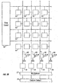
- FIG. 2 shows a focal plane array of many cells 10 formed on a silicon substrate 20.
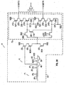
- FIG. 3A is a simplified schematic diagram of a pixel cell 10 and its associated processing.
- Each pixel cell 10 includes a photogate area and its associated circuitry (30 - 50) and row decoder elements 55,60.
- FIG. 3A shows the photogate 12 having a relatively large photogate electrode 30 overlying the substrate.
- the charge transfer section 14 has a transfer gate electrode 35 adjacent the photogate electrode 30, a floating diffusion 40, a reset electrode 45 and a drain diffusion 50.
- the readout circuit 16 has a source follower field effect transistor (FET) 55, a row select FET 60, a load FET 65 and a correlated double sampling circuit 70.
- FET source follower field effect transistor
- the surface potential diagram of FIG. 4 shows the photogate electrode 30 being held by a photogate signal PG at a positive voltage to form a potential well 80 in the substrate 20 in which photo-generated charge is accumulated during an integration period.
- the transfer gate electrode 35 is initially held at a less positive voltage by a transfer gate signal TX to form a potential barrier 85 adjacent the potential.well 80.
- the floating diffusion 40 is connected to the gate of the source follower FET 55 whose drain is connected to a drain supply voltage VDD.
- the reset electrode 45 is initially held by a reset signal RST at a voltage corresponding to the voltage on the transfer gate 30 to form a potential barrier 90 thereunder.
- the drain supply voltage VDD connected to the drain diffusion 50 creates a constant potential well 95 underneath the drain diffusion 50.
- the surface potential beneath the floating diffusion 40 is quickly reset to a potential level 100 slightly above the potential well 95. This is accomplished by the reset signal RST temporarily increasing to a higher positive voltage to temporarily remove the potential barrier 90 and provide a downward potential staircase from the transfer gate potential barrier 85 to the drain diffusion potential well 95, as indicated in the drawing of FIG. 4.
- the readout circuit 70 briefly samples the potential of the floating diffusion 40, and then the cell 10 is ready to transfer the photo-generated charge from beneath the photogate electrode 30.
- the photogate signal PG decreases to a less positive voltage to form a potential barrier 105 beneath the photogate electrode 30 and thereby provide a downward staircase surface potential from the photogate electrode 30 to the potential well 100 beneath the floating diffusion 40.
- This operation transfers the charge from beneath the photogate electrode 30 to the floating diffusion 40, changing the potential of the floating diffusion 40 from the level. (100) at which it was previously reset to.a new level 107 indicative of the amount of charge accumulated during the integration period.
- This new potential of the floating diffusion 40 is sensed at the source of the source follower FET 55.
- the photogate signal PG returns to its initial (more positive) voltage. The entire process is repeated for the next integration period.
- the readout circuit 70 has a signal sample and hold (S/H) circuit including an S/H FET 200 and a signal store capacitor 205 connected through the S/H FET 200 and through the row select FET 60 to the source of the source follower FET 55.
- the other side of the capacitor 205 is connected to a source bias voltage VSS.
- the one side of the capacitor 205 is also connected to the gate of an output FET 210.
- the drain of the output FET is a connected through a column select FET 220 to a signal sample output node VOUTS and through a load FET 215 to the drain voltage VDD.
- a signal called “signal sample and hold” (SHS) briefly turns on the S/H FET 200 after the charge accumulated beneath the photogate electrode 30 has been transferred to the floating diffusion 40, so that the capacitor 205 stores the source voltage of the source follower FET 55 indicating the amount of charge previously accumulated beneath the photogate electrode 30.
- SHS signal sample and hold
- the readout circuit 70 also has a reset sample and hold (S/H) circuit including an S/H FET 225 and a signal store capacitor 230 connected through the S/H FET 225 and through the row select FET 60 to the source of the source follower FET 55.
- the other side of the capacitor 230 is connected to the source bias voltage VSS.
- the one side of the capacitor 230 is also connected to the gate of an output FET 240.
- the drain of the output FET 240 is connected through a column select FET 245 to a reset sample output node VOUTR and through a load FET 235 to the drain voltage VDD..
- a signal called "reset sample and hold" (SHR) briefly turns on the S/H FET 225. immediately after the reset signal RST has caused the resetting of the potential of the floating diffusion 40, so that the capacitor 230 stores the voltage to which the floating diffusion has been reset.
- the readout circuit provides a special form of correlated double sampling of the potential of the floating diffusion, allowing the charge integrated beneath the photogate 12 during each integration period to be obtained at the end of each integration period from the difference between the voltages at the output nodes VOUTS and VOUTR of the readout circuit 70.
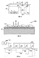
- FIG. 5 shows a transparent refractive microlens layer 110 which may be deposited over the top of the focal plane array of FIG. 2.
- the microlens layer 110 has spherical portions 115 centered over each of the cells 10 and contoured so as to focus light toward the center of each photogate 12. This has the advantage of using light that would otherwise fall outside of the optically active region of the photogate 12. For example, at least some of the light that is ordinarily incident on either the charge transfer section 14 or the readout circuit 16 (FIG. 1) would be sensed in the photogate area with the addition of the microlens layer 110. This has the effect of maximizing real estate - the portions of the substrate which include the non-photogate area are focused to another point.
- FIG.s 6A and 6B show an alternative embodiment which uses color filtering.
- Color filtering enables spatial separation of color in an imaging device.
- CCD devices for example, commonly use kind of color separation in this way.
- the preferred system allows a plurality of pixels to have different color filtering properties to provide a color filtering effect. Typically this is done by using the color filters in some array form: For example, alternate green filters interspersed with red and blue filters. An exemplary filter operation would use green/red/green/blue/green/red/green/blue with that pattern continuing for the length of the array.
- color filters are used to supplement the lens operation of FIG. 5.
- the preferred system embodies its operation in one of the two forms shown in FIG.s 6A and 6B.
- the first form shown in FIG. 6A uses a polymer color filter array.
- Layer 600 is preferably a red layer, and is first deposited over the entire chip. Subsequent to deposition, an et ching technique is used to remove the red filter area 600 from everywhere except over the desired pixel 10.
- a planarization layer 602 covers the removed areas to thereby planarize that surface, thereby flattening the surface.
- Blue filter 604 is next deposited over pixel 10A. Blue filter 604 is similarly etched such that it only covers the desired pixel 10A. The remaining area is planarized by a second planarization layer 606. Finally, a green filter 610 is formed over that planarized layer, covering pixel 10B. Planarization layer 612 flattens the resulting area so that green filter 610 only covers the pixel 10B.
- Each pixel, including the polymer layer, is covered by microlens 115A; 115B and 115C.
- the microlenses modify the incoming light in conjunction with the polymer layer. The light is therefore changed by both microlenses 115A-115C and CFA parts 610, 604, and 600.
- Each pixel therefore, preferably receives light that has been altered by the lens and altered by the color filter array.
- This polymer color filter array sacrifices a certain amount of resolution of the scene.
- Each pixel of the scene is imaged by three pixels, and hence some of the pixels are dedicated to a different color.
- FIG. 6B An alternative embodiment shown in FIG. 6B does not lose resolution, but instead requires multiple chips to form any image. This would form a 3-chip camera.
- One chip 650 has all its pixels covered by a red filter 620. Hence that chip images the red scene - either the red components or the complement to the red components. Analogously, the other chips include green filters and blue filters. The three chips together form the entire image.
- a wavelength-converting phosphor is typically tuned to accept radiation of a desired wavelength, e.g.,, ultra-violet or x-ray.
- a desired wavelength e.g., ultra-violet or x-ray.
- the silicon underlayer is not responsive to that same wavelength. Therefore, the phosphor emits a photon of the proper type to properly excite the underlying silicon 662, when receiving this radiation.
- the phosphor 660 is sensitive to x-ray, but emits a photon of green light that is detected by the circuitry 662 which can be a sensor of any of the kinds described herein.
- FIG. 6C embodiment contemplates using the wavelength-converting phosphor over an entire surface of the device, it is also possible to use a pixelation effect.
- a shadow mask is used to mask the phosphor. The phosphor is only deposited where allowed by the shadow mask.
- the focal plane array corresponding to FIG.s 1-4 is implemented in MOS silicon or CMOS, or any other technology which is compatible with an industry standard CMOS fabrication process.
- each of the FETs is a MOSFET, the FETs 55, 60, 65, 200 and 225 being n-channel devices and the FETs 210, 220, 215, 235, 240, 245 being p-channel devices.
- the n-channel MOSFETS and the CCD channel underlying the gate electrodes 30, 35, 45 and the diffusions 40 and 50 may be located in a p-well while the remaining (p-channel) devices are located outside of the p-well.
- the gate voltage VLP applied to the gates of the p-channel load FETs 215 and 235 is a constant voltage on the order of +2.5 volts.
- the gate voltage VLN applied to the n-channel load FET 65 is a constant voltage on the order of +1.5 volts.
- the charge transfer section 14 preferably uses only a single CCD stage between the photogate 12 and the floating diffusion 40 in the specific embodiment of FIG. 3A. This means that there is no loss due to charge transfer inefficiency and therefore there is no need to fabricate the device with a special CCD process.
- the readout circuit 70 as well as the output circuitry of the FETs 55, 60 and 65 can be readily implemented as standard CMOS circuits, making them relatively inexpensive.
- any suitable charge coupled device architecture may be employed to implement the charge transfer section 14, including a CCD having more than one stage. For example, two or three stages may be useful for buffering two or three integration periods.
- the floating diffusion 40 may instead be a floating gate electrode.
- the signal and reset sample and hold circuits of the readout circuit 70 may be any suitable sample and hold circuits.
- shielding of the type well-known in the art may be employed defining an aperture surrounding the photogate 12.
- the invention may be implemented as a buried channel, n-well, or p-channel device.
- Another feature of the invention which is useful for eliminating fixed pattern noise due to variations in FET threshold voltage across the substrate 20 is a shorting FET 116 across the sampling capacitors 205, 235.
- a shorting signal VM is temporarily applied to the gate of the shorting FET 116 and the VOUTS-to-VOUTR difference is measured again.
- This latter difference is a measure of the disparity between the threshold voltages of the output FETs 210, 240, and may be referred to as the fixed pattern difference.
- the fixed pattern difference is subtracted from the difference between VOUTS and VOUTR measured at the end of the integration period, to remove fixed pattern noise.
- a floating gate may be used instead of the floating diffusion 40.
- a floating gate is indicated schematically in FIG. 3A by a simplified dashed line floating gate electrode 41.
- the area of the photogate 12 i.e., the photogate electrode 30
- the photogate electrode 30 is preferably L-shaped as shown in FIG.
- the transfer gate electrode 35 and the reset gate electrode were each about 1.5 microns by about 6 microns;
- the photogate signal PG was varied between about +5 volts (its more positive voltage) and about 0 volts (its less positive voltage;
- the transfer gate signal TX was about +2.5 volts;
- the reset signal RST was varied between about +5 volts (its more positive voltage) and about +2.5 volts (its less positive voltage);
- the drain diffusion 50 was held at about +5 volts.
- the array structure of FIG.s 1-4 can be modified to incorporate a preferred column parallel approach.
- column parallel approach refers to a portion of the readout circuitry being connected to the bottom on the columns of the array. This allows an entire row of the array to be processed at one time.
- This column approach is in contrast to a spatially parallel processing approach where each pixel has its own processing circuitry (e.g., the embodiment of FIG.s 1-4), or a serial processing approach where the output of each pixel is sequentially feed to a single processor for processing.
- FIG. 3B shows a column parallel approach where the load FET 65 and correlated double sampling circuit 70 are deleted from the individual pixel cells 10. Instead, each cell 10 in a column of the array is connected to a common load FET 65 and sampling circuit 70. The common elements are preferably located at the bottom of each column of the array.
- This column parallel array structure has a significant advantage. Since the load FET 65 and sampling circuit 70 have been removed from the pixel cells 10, there is more photosensitive cell area available. Thus, the resolution of each cell 10 is improved.
- the column parallel array structure is read out by selecting an entire row using standard row and column select circuitry 18, 19. Selecting a row, among other things, results in the accumulated charge being transferred from the photogate potential well 80 of each cell 10 in the row to its associated floating diffusion 40. Thereafter, the sampling circuits 70 at the bottom of each column "read” the connected pixel cell 10 in the manner described previously..
- a standard multiplexer 21 is then employed to output the "read" pixel cell values, either in parallel or serially.
- the previous described pixel cell structure of FIG.s 3A or 3B and 4 can be further modified to include simultaneous integration of the array.
- charge accumulated in the photogate well 80 during the integration period was transferred directly to the floating diffusion 40.
- not all the cells in the array could be read out at the same time. The charge that was transferred to the floating diffusion 40 would degrade over time.
- One counter measure to this problem is to transfer only the accumulated charge for pixel cells that are currently being read out. For example, as described in connection with the embodiment of fig. 3B, only a row of the array is read out at one time. However, since only a portion of the array is read out, the resulting image from all the cells represents a series of lines, each corresponding to the observed scene at a different time. If the observed scene is changing, the resulting image may be motion-skewed, i.e., may have some portions that represent a different instant of time than others. At the same time, it is important that noise be minimized.
- FIG. 6 shows an embodiment that accomplishes these goals according to the technique of the present invention, by incorporating additional structure into the basic cell structure.
- a storage gate electrode 260 overlies a storage potential well 265 in the substrate.
- the storage well 265 is a supplemental charge storage area which stores charge from the main light collection area '-- photogate well 80.
- the size of storage well 265 depends on the necessary charge amount. In low light situations, for example, the area of the optical charge storage area may need to be large in order to collect as much light as possible. However, the charge storage area may never fill. In that case, storage well needs only enough area to store the intended amount of charge.
- storage well 265 preferably has a similar surface area as the photogate well 80 to ensure that all the charge accumulated in the photogate well 80 can be transferred to the storage well 265.
- the non-photosensitive portion of the pixel cell is preferably shielded from optical radiation by an opaque layer 270, e.g., a metal layer.
- the non-photosensitive portion of the cell includes.the area underlying the intermediate transfer gate 255 and storage gate 260, as well as the transfer gate 35, floating diffusion 40, reset gate 45, and V + drain 50.
- This optical shielding layer 270 minimizes the possibility that optically generated noise affects the charge stored in the storage well 265, or the other identified structures.
- a control system 700 supplies voltage.
- the charge accumulated in the photogate well 80 under the photogate electrode 30 during the integration period is then transferred across the intermediate transfer gate 255 and into the storage potential well 265.
- the charge remains in well 265 until readout.
- the voltage VPg on the photogate electrode 30 is initially greater than the voltage VTg of intermediate transfer gate 255.
- VPg is reduced to less than VTg. This forms potential barrier 105 beneath the photogate electrode 30, thereby providing a downward staircase surface potential from the photogate electrode 30 to the storage well 265 which is being held at a higher positive voltage than the intermediate transfer gate 255.
- the floating diffusion node 40 is reset and the reset voltage sampled, as discussed previously.
- the charge is transferred from the storage well 265 over the transfer gate potential 85 and into the floating diffusion node 40, where it is sampled, in the same way the charge was transferred from the photogate well 80 to the node 40 in the first-described embodiment of FIG.s 3A-B and 4.
- the techniques of the storage well 265 and transferring of the charge from the photogate well 80 to the storage well 265 after the integration period enables simultaneous integration.
- the accumulated charge in each cell is transferred.to its associated storage well 265 at the end of the integration period. Therefore, all the pixel cells, or a part as desired, can be used to image the observed scene for the duration of the prescribed integration period, regardless of when each individual cell is to be.read out. This allows a "snapshot" image to be stored.
- the storage well 265 provides a stable structure in which to store the transferred charge.
- an important part of the present invention is the ability to store shuttered information in a way that still allows correlated double sampling.
- the system of the present invention enables a more accurate detection than that which has been available previously.
- the accumulated and transferred charge can remain in the storage well 265, preferably substantially isolated from noise or leakage, until the time of readout for that cell.
- the charge is transferred to the floating diffusion 40.
- This simultaneous integration pixel cell structure trades off the ability to store a snapshot against the fill factor of the cell.
- the intermediate transfer gate 255 and storage gate 260 take up room on the substrate and are shielded from optical radiation. Therefore, the proportion of the cell that is actively photosensitive is reduced. This may have the effect of lowering the resolution of the cell for any particular cell size.
- FIG. 6A shows one particular pixel, including a photosensitive part, and a non-photosensitive part. As described in the preferred embodiment, the non-photosensitive part is covered by blocking layer 270. Planarization layer 602, 606, 612, preferably transparent layer which does not affect the optical radiation passing therethrough, covers the photosensitive portion. This forms a flat surface.
- a color filter 600, 604, 610 is optionally formed over the planarized layer including the optical blocking layer and the planarization layer.
- FIG. 6A shows the color filter formed over the entire pixel, but it should be understood that the color filter need not cover the entire pixel since part of this is blocked.
- lens 115a-115c which is formed to refract light incoming from over the non-photosensitive area 612 towards the photosensitive area 610.
- This lens can recapture some of the light which would otherwise fall on the shielded area and refract it to increase some of the resolution.
- Shutter gate 302 and a shutter drain diffusion 304 are positioned relative to the photogate 30 to bleed off charge away from the photogate.
- the shutter drain diffusion 304 may also act as the previously described V+ drain 50, either for the same pixel or of an adjacent pixel in the array, In either case, the shutter drain diffusion 304 is maintained at a positive voltage exceeding the potential of the other gates to form a potential well shown as 300 under drain diffusion 304.
- the shutter gate 302 and shutter drain diffusion 304 act together to selectively prevent charge accumulation in the associated pixel or allow the accumulation of an optically generated charge under the photogate 30 when desired. Accumulation of charge is prevented by biasing shutter gate 302 to a positive voltage which exceeds the bias on the photogate 30. This forms a potential barrier 306. At the same time the bias on the transfer gate 35 is made less than that on the photogate electrode 30 to form potential barrier 308. This creates a downward staircase in surface potential from the photogate electrode 30 via well 306 to the potential well 300 beneath the shutter drain diffusion 304. This downward staircase allows any optically generated charge in the photogate potential well 80 spills across the shutter gate 302 into potential well 300 and into shutter drain diffusion 304. In this mode, the electronic shutter is effectively "closed” since optically generated charge is not allowed to accumulate.
- the shutter gate bias is changed to a voltage lower than the photogate 30, but slightly higher than the transfer gate 35. This forms potential barrier 310.
- the inventors prefer making the shutter gate bias slightly higher than that of the transfer gate 35.
- the photogate potential well 80 fills until charge begins to flow over the shutter gate potential 310 into the shutter drain diffusion 304. Therefore, charge does not leak past the transfer gate potential 308 and into the floating diffusion node 40 where it could disrupt the readout process described earlier.
- This specific expedient allows a lateral anti-blooming control in the pixel cell and provides an.additional advantage to the electronic shutter structure.
- the charge accumulated under the photogate 30 is shifted to the floating diffusion node 40 (or storage well) by lowering the shutter gate bias to a voltage below the bias voltage of the transfer gate 35 to form potential barrier 312, and then pulsing the photogate bias to a similar lower voltage to form potential barrier 314.
- This causes the charge accumulated during the selected integration period to flow over the transfer gate potential 308 and into the floating diffusion node 40.
- the electronic shutter can be closed once again, or a new integration cycle can be initiated by adjusting the shutter gate and photogate biases as described above.
- the section of the pixel cell from the diffusion node 40 side edge of the photogate 30, through the transfer gate 35, floating diffusion node 40, reset gate 45, and V+ drain 50 is preferably covered with an opaque layer 316, such as one made of metal, to block optical radiation and reduce optically-generated noise in the underlying substrate.
- the shutter gate 302 is biased to the V+ drain potential (i.e., about 5 volts), the photogate 30 is biased to about 4 volts, and the transfer gate. 35 is biased to about 1.2 volts, in the "closed” mode.
- the shutter gate potential is changed to about 1.5 volts, while the other gate potentials remain the same.
- the accumulated charge is transferred to the floating diffusion node 40, by setting the shutter gate 302 at 0 volts and the photogate 30 is pulsed to this same potential.
- the electronic shutter makes it possible to set a desired integration time for all or some of the cells.
- the integration time for any one cell is set by simply "opening" the electronic shutter for a predetermined period of time.
- the pixel cell in FIG. 7 uses overlapping gates 318.
- the photogate 30 overlaps the shutter gate 302, and transfer gate 35, over the surface of the pixel cell substrate.
- This overlapping gate structure enhances the charge transfer efficiency discussed previously. This enhancement results from reducing the area of the substrate that would otherwise have to exist between adjacent gates. This area is placed under the influence of one of the gate potentials. Accordingly, the charge transfer is facilitated.
- the formation of overlapping gates 318 in a CMOS device requires a double poly process. Advanced CMOS fabrication processes which use only a single layer of poly can be used. Therefore, spaced gates with intervening gaps are a necessity in these single poly layer CMOS implementations. In such a structure, floating diffusions 320 are created in the substrate under the gaps 322 between the photogate 30, shutter gate 302, and the transfer gate 35, as shown in FIG. 8.
- Any overlap described herein can be replaced a floating diffusion with non-overlapping poly from a single poly layer.
Landscapes
- Engineering & Computer Science (AREA)
- Multimedia (AREA)
- Signal Processing (AREA)
- Solid State Image Pick-Up Elements (AREA)
Claims (11)
- Dispositif imageur comprenant :une pluralité de pixels imageurs (10) formés sur un substrat (20), chaque pixel imageur comprenant :une zone de collecte de lumière (12) pour recevoir un rayonnement, comprenant une électrode de grille photonique (30) et une zone de stockage de grille photonique (80) qui est commandée par ladite électrode de grille photonique (30) pour accumuler des charges produites par une radiation reçue ;une zone de stockage de charges supplémentaire (265) physiquement adjacente et séparée de ladite zone de collecte de lumière (12) pour recevoir et stocker des charges de ladite zone de collecte de lumière (12), dans laquelle ladite zone de stockage de charges supplémentaire (265) a une capacité de stockage permettant de recevoir toutes les charges accumulées dans ladite zone de collecte de lumière (12) ;un mécanisme à transfert de charges, couplé entre ladite zone de collecte de lumière (12) et ladite zone de stockage de charges supplémentaire (265), ledit mécanisme à transfert de charges comprenant un dispositif utilisable (255) qui est utilisable sélectivement pour transférer des charges dans ladite zone de collecte de lumière (12) vers ladite zone de stockage de charges supplémentaire (265) ;un noeud de sortie (40), connecté pour recevoir des charges de ladite zone de stockage de charges supplémentaire (265) pour produire une sortie représentant les charges reçues, et étant électriquement flottant lorsqu'il n'est pas connecté ; etun second mécanisme à transfert de charges (35) situé entre ladite zone de stockage de charges supplémentaire (265) et ledit noeud de sortie (40) et utilisable pour transférer des charges de ladite zone de stockage de charges supplémentaire (265) vers ledit noeud de sortie (40).
- Dispositif selon la revendication 1, comprenant en outre des moyens pour une intégration simultanée pour commander les électrodes de grille photonique (30) desdits pixels imageurs (10) pour commencer un nouveau cycle d'intégration pour collecter des charges dans chaque zone de stockage de grille photonique (80) après que les charges accumulées dans chaque zone de stockage de grille phonique (80) dans le précédent cycle d'intégration aient été transférées à leur zone de stockage de charges supplémentaire (265) pour une sortie vers le noeud de sortie (40).
- Dispositif selon la revendication 1, comprenant en outre un double élément d'échantillonnage corrélé (70) pour échantillonner une tension sur ledit noeud de sortie (40) avant le transfert des charges vers celui-ci, et pour échantillonner une tension sur ledit noeud de sortie (40) après le transfert des charges vers celui-ci pour produire une sortie pour chaque pixel imageur (10) sans bruit associé avec chaque pixel imageur (10).
- Dispositif selon la revendication 1, dans lequel ladite zone de collecte de lumière (12) a une zone qui est sensiblement la même qu'une zone de ladite zone de stockage de charges supplémentaire (265).
- Dispositif selon la revendication 1, comprenant en outre un écran optique (270) couvrant optiquement au moins une partie de ladite zone de stockage de charges supplémentaire (265).
- Dispositif selon la revendication 5 comprenant en outre une microlentille (110) recouvrant l'écran optique (270) et réfractant au moins une partie de la lumière empiétant sur une zone dudit écran optique (270) jusqu'à ladite zone de collecte de lumière (12).
- Dispositif selon la revendication 1, comprenant en outre un obturateur électronique pour chaque pixel imageur (10), ledit obturateur électronique comprenant :une diffusion d'obturateur (304) située de manière adjacente à ladite zone de stockage de grille photonique (80) ; etune grille d'obturateur (302) située entre ladite zone de stockage de grille photonique (80) et ladite diffusion d'obturateur (304) pour commander le transfert de charges de ladite zone de stockage de grille photonique (80) à ladite diffusion d'obturateur (304) ; etdes moyens pour commander un potentiel électrique sur ladite grille d'obturateur (302) à une première valeur (306) pour transférer n'importe quelle charge dans ladite zone de stockage de grille photonique (80) vers ladite diffusion d'obturateur (304) pour couper ledit pixel imageur (10), à une seconde valeur (310) pour permettre à des charges de s'accumuler dans ladite zone de stockage de grille photonique (80) et pour être transférées vers ladite zone de stockage de charges supplémentaire (265) pour leur lecture, et à une troisième valeur (312) pour limiter une quantité de charges accumulées dans ladite zone de stockage de grille photonique (80) comme mécanisme anti-éblouissement.
- Dispositif selon la revendication 7, dans lequel chacun des pixels imageurs (10) comprend en outre une diffusion de drain (50) située de manière adjacente audit noeud de sortie (40) pour drainer des charges depuis ledit noeud de sortie (40) après qu'un niveau de sortie au niveau dudit noeud de sortie (40) a été lu, dans lequel ladite diffusion de drain (50) est connectée à ladite diffusion d'obturateur (304) dans ledit pixel imageur (10).
- Dispositif selon la revendication 7, dans lequel chaque pixel imageur (10) comprend en outre une grille de réinitialisation (45) située entre ledit noeud de sortie (40) et une diffusion d'obturateur (304) d'un pixel imageur adjacent (10) et utilisable pour drainer des charges depuis ledit noeud de sortie (40) à ladite diffusion d'obturateur (304) dudit pixel imageur adjacent (10) après qu'un niveau de sortie au niveau dudit noeud de sortie (40) a été lu.
- Dispositif selon la revendication 1, comprenant en outre :un circuit de commande (700) pour indiquer aux électrodes de grille photonique (30) desdits pixels imageurs (10) d'accumuler simultanément des charges d'une scène d'entrée au cours d'une période d'intégration et d'initier une autre intégration dans chacun desdits pixels imageurs (10) après que les charges accumulées dans chaque zone de stockage de grille photonique (80) à la fin de ladite période d'intégration ont été transférées dans une zone de stockage de charges supplémentaire respective (265),dans lequel ledit circuit de commande (700) commande la lecture depuis les zones de stockage de charges supplémentaires (265) à différents moments pour former une image instantanée capturée simultanément par différents pixels imageurs (10) au cours de ladite période d'intégration.
- Dispositif selon la revendication 10, dans lequel chaque pixel imageur (10) comprend en outre :un piège à charges adjacent à ladite zone de stockage de grille photonique (80) et utilisable pour recevoir une certaine quantité de charges depuis ladite zone de stockage de grille photonique (80) de manière à empêcher ladite certaine quantité de charges d'être couplées à ladite zone de stockage de charges supplémentaire (265) ; etun élément de transfert disposé relativement audit piège à charges et à ladite zone de stockage de grille photonique (80), et configuré pour commander le transfert de charges depuis ladite zone de stockage de grille photonique (80) vers ledit piège à charges, ledit élément de transfert étant fixé à un potentiel pour empêcher les charges accumulées dans ladite zone de stockage de grille photonique (80) au-delà d'un niveau maximum d'être couplées dans ladite zone de stockage de charges supplémentaire (265).
Applications Claiming Priority (5)
| Application Number | Priority Date | Filing Date | Title |
|---|---|---|---|
| US1030596P | 1996-01-22 | 1996-01-22 | |
| US10305P | 1996-01-22 | ||
| US1370096P | 1996-03-20 | 1996-03-20 | |
| US13700P | 1996-03-20 | ||
| EP97903876A EP0878007B1 (fr) | 1996-01-22 | 1997-01-22 | Reseau de detecteurs a pixels actifs obturables electroniquement |
Related Parent Applications (1)
| Application Number | Title | Priority Date | Filing Date |
|---|---|---|---|
| EP97903876A Division EP0878007B1 (fr) | 1996-01-22 | 1997-01-22 | Reseau de detecteurs a pixels actifs obturables electroniquement |
Publications (3)
| Publication Number | Publication Date |
|---|---|
| EP1505823A2 EP1505823A2 (fr) | 2005-02-09 |
| EP1505823A3 EP1505823A3 (fr) | 2005-02-23 |
| EP1505823B1 true EP1505823B1 (fr) | 2007-05-02 |
Family
ID=33555971
Family Applications (1)
| Application Number | Title | Priority Date | Filing Date |
|---|---|---|---|
| EP04077767A Expired - Lifetime EP1505823B1 (fr) | 1996-01-22 | 1997-01-22 | Reseau de detecteurs a pixels actifs |
Country Status (1)
| Country | Link |
|---|---|
| EP (1) | EP1505823B1 (fr) |
Families Citing this family (1)
| Publication number | Priority date | Publication date | Assignee | Title |
|---|---|---|---|---|
| US20080106625A1 (en) * | 2006-11-07 | 2008-05-08 | Border John N | Multi image storage on sensor |
Family Cites Families (5)
| Publication number | Priority date | Publication date | Assignee | Title |
|---|---|---|---|---|
| US4873561A (en) * | 1988-04-19 | 1989-10-10 | Wen David D | High dynamic range charge-coupled device |
| JPH0766961B2 (ja) * | 1988-10-07 | 1995-07-19 | 三菱電機株式会社 | 固体撮像素子 |
| US5355165A (en) * | 1992-08-06 | 1994-10-11 | Princeton Scientific Instruments, Inc. | Very high frame rate CCD imager |
| US5471515A (en) * | 1994-01-28 | 1995-11-28 | California Institute Of Technology | Active pixel sensor with intra-pixel charge transfer |
| US5541402A (en) * | 1994-10-17 | 1996-07-30 | At&T Corp. | Imaging active pixel device having a non-destructive read-out gate |
-
1997
- 1997-01-22 EP EP04077767A patent/EP1505823B1/fr not_active Expired - Lifetime
Also Published As
| Publication number | Publication date |
|---|---|
| EP1505823A3 (fr) | 2005-02-23 |
| EP1505823A2 (fr) | 2005-02-09 |
Similar Documents
| Publication | Publication Date | Title |
|---|---|---|
| US6825059B2 (en) | Active pixel sensor array with electronic shuttering | |
| EP0878007B1 (fr) | Reseau de detecteurs a pixels actifs obturables electroniquement | |
| US6166768A (en) | Active pixel sensor array with simple floating gate pixels | |
| US5990506A (en) | Active pixel sensors with substantially planarized color filtering elements | |
| US7105371B2 (en) | Method of acquiring an image from an optical structure having pixels with dedicated readout circuits | |
| US5949483A (en) | Active pixel sensor array with multiresolution readout | |
| US6046466A (en) | Solid-state imaging device | |
| KR101776955B1 (ko) | 고체 촬상 장치와 그 제조 방법, 및 전자 기기 | |
| US9748298B2 (en) | Image sensors with backside trench structures | |
| EP2253016B1 (fr) | Pixel de référence noir pour un détecteur d'image rétroéclairé | |
| US20090201400A1 (en) | Backside illuminated image sensor with global shutter and storage capacitor | |
| CN111430388A (zh) | 成像像素 | |
| KR20110109873A (ko) | 고체 촬상 장치, 고체 촬상 장치의 제조 방법, 및 전자 기기 | |
| CN111491115A (zh) | 像素具有高动态范围、动态电荷溢流和全局快门扫描的背照式图像传感器 | |
| US10855939B1 (en) | Stacked image sensor with programmable edge detection for high frame rate imaging and an imaging method thereof | |
| US20150295007A1 (en) | Image sensor with dielectric charge trapping device | |
| CN110520993A (zh) | 摄像装置和电子设备 | |
| TWI413246B (zh) | 在一互補式金氧半導體像素中之半島形傳送閘 | |
| US9853080B2 (en) | Pixels with multiple charge storage regions | |
| US20100214464A1 (en) | Solid-state imaging apparatus | |
| CN101950752B (zh) | 固态成像装置和电子装置 | |
| US20060208159A1 (en) | Producing method for solid-state image pickup device | |
| EP1505823B1 (fr) | Reseau de detecteurs a pixels actifs | |
| CN210093338U (zh) | 图像传感器 | |
| CN121000984A (zh) | 用于光电二极管的复位栅极 |
Legal Events
| Date | Code | Title | Description |
|---|---|---|---|
| PUAI | Public reference made under article 153(3) epc to a published international application that has entered the european phase |
Free format text: ORIGINAL CODE: 0009012 |
|
| PUAL | Search report despatched |
Free format text: ORIGINAL CODE: 0009013 |
|
| 17P | Request for examination filed |
Effective date: 20041022 |
|
| AC | Divisional application: reference to earlier application |
Ref document number: 0878007 Country of ref document: EP Kind code of ref document: P |
|
| AK | Designated contracting states |
Kind code of ref document: A2 Designated state(s): DE FR GB IE IT NL SE |
|
| AK | Designated contracting states |
Kind code of ref document: A3 Designated state(s): DE FR GB IE IT NL SE |
|
| RIN1 | Information on inventor provided before grant (corrected) |
Inventor name: FOSSUM, ERIC R. |
|
| AKX | Designation fees paid |
Designated state(s): DE FR GB IE IT NL SE |
|
| GRAP | Despatch of communication of intention to grant a patent |
Free format text: ORIGINAL CODE: EPIDOSNIGR1 |
|
| RIN1 | Information on inventor provided before grant (corrected) |
Inventor name: FOSSUM, ERIC R. |
|
| GRAS | Grant fee paid |
Free format text: ORIGINAL CODE: EPIDOSNIGR3 |
|
| GRAA | (expected) grant |
Free format text: ORIGINAL CODE: 0009210 |
|
| AC | Divisional application: reference to earlier application |
Ref document number: 0878007 Country of ref document: EP Kind code of ref document: P |
|
| AK | Designated contracting states |
Kind code of ref document: B1 Designated state(s): DE FR GB IE IT NL SE |
|
| REG | Reference to a national code |
Ref country code: GB Ref legal event code: FG4D |
|
| REG | Reference to a national code |
Ref country code: IE Ref legal event code: FG4D |
|
| REF | Corresponds to: |
Ref document number: 69737705 Country of ref document: DE Date of ref document: 20070614 Kind code of ref document: P |
|
| PG25 | Lapsed in a contracting state [announced via postgrant information from national office to epo] |
Ref country code: SE Free format text: LAPSE BECAUSE OF FAILURE TO SUBMIT A TRANSLATION OF THE DESCRIPTION OR TO PAY THE FEE WITHIN THE PRESCRIBED TIME-LIMIT Effective date: 20070802 |
|
| ET | Fr: translation filed | ||
| PLBE | No opposition filed within time limit |
Free format text: ORIGINAL CODE: 0009261 |
|
| STAA | Information on the status of an ep patent application or granted ep patent |
Free format text: STATUS: NO OPPOSITION FILED WITHIN TIME LIMIT |
|
| 26N | No opposition filed |
Effective date: 20080205 |
|
| REG | Reference to a national code |
Ref country code: FR Ref legal event code: PLFP Year of fee payment: 20 |
|
| PGFP | Annual fee paid to national office [announced via postgrant information from national office to epo] |
Ref country code: GB Payment date: 20151215 Year of fee payment: 20 |
|
| PGFP | Annual fee paid to national office [announced via postgrant information from national office to epo] |
Ref country code: FR Payment date: 20151230 Year of fee payment: 20 |
|
| PGFP | Annual fee paid to national office [announced via postgrant information from national office to epo] |
Ref country code: NL Payment date: 20160118 Year of fee payment: 20 |
|
| PGFP | Annual fee paid to national office [announced via postgrant information from national office to epo] |
Ref country code: IE Payment date: 20160119 Year of fee payment: 20 Ref country code: IT Payment date: 20160128 Year of fee payment: 20 Ref country code: DE Payment date: 20160119 Year of fee payment: 20 |
|
| REG | Reference to a national code |
Ref country code: DE Ref legal event code: R071 Ref document number: 69737705 Country of ref document: DE |
|
| REG | Reference to a national code |
Ref country code: NL Ref legal event code: MK Effective date: 20170121 |
|
| REG | Reference to a national code |
Ref country code: GB Ref legal event code: PE20 Expiry date: 20170121 |
|
| REG | Reference to a national code |
Ref country code: IE Ref legal event code: MK9A |
|
| PG25 | Lapsed in a contracting state [announced via postgrant information from national office to epo] |
Ref country code: IE Free format text: LAPSE BECAUSE OF EXPIRATION OF PROTECTION Effective date: 20170122 Ref country code: GB Free format text: LAPSE BECAUSE OF EXPIRATION OF PROTECTION Effective date: 20170121 |