EP1507169A1 - Lichtempfindliche Dickschichtmaterialien in Pastenform zur Herstellung lichtdurchlässiger elektromagnetischer Abschirmungen, daraus hergestellte lichtdurchlässige elektromagnetische Abschirmungen und Verfahren zu deren Herstellung - Google Patents
Lichtempfindliche Dickschichtmaterialien in Pastenform zur Herstellung lichtdurchlässiger elektromagnetischer Abschirmungen, daraus hergestellte lichtdurchlässige elektromagnetische Abschirmungen und Verfahren zu deren Herstellung Download PDFInfo
- Publication number
- EP1507169A1 EP1507169A1 EP04018685A EP04018685A EP1507169A1 EP 1507169 A1 EP1507169 A1 EP 1507169A1 EP 04018685 A EP04018685 A EP 04018685A EP 04018685 A EP04018685 A EP 04018685A EP 1507169 A1 EP1507169 A1 EP 1507169A1
- Authority
- EP
- European Patent Office
- Prior art keywords
- nickel
- light
- regions
- film
- transmitting electromagnetic
- Prior art date
- Legal status (The legal status is an assumption and is not a legal conclusion. Google has not performed a legal analysis and makes no representation as to the accuracy of the status listed.)
- Withdrawn
Links
- 238000000034 method Methods 0.000 title claims description 47
- 239000000463 material Substances 0.000 title claims description 20
- 238000004519 manufacturing process Methods 0.000 title description 13
- 239000000203 mixture Substances 0.000 claims description 77
- PXHVJJICTQNCMI-UHFFFAOYSA-N Nickel Chemical compound [Ni] PXHVJJICTQNCMI-UHFFFAOYSA-N 0.000 claims description 72
- 239000011230 binding agent Substances 0.000 claims description 67
- 239000011521 glass Substances 0.000 claims description 57
- 239000000758 substrate Substances 0.000 claims description 53
- BQCADISMDOOEFD-UHFFFAOYSA-N Silver Chemical compound [Ag] BQCADISMDOOEFD-UHFFFAOYSA-N 0.000 claims description 52
- 229910052709 silver Inorganic materials 0.000 claims description 51
- 239000004332 silver Substances 0.000 claims description 51
- BASFCYQUMIYNBI-UHFFFAOYSA-N platinum Chemical compound [Pt] BASFCYQUMIYNBI-UHFFFAOYSA-N 0.000 claims description 46
- KDLHZDBZIXYQEI-UHFFFAOYSA-N Palladium Chemical compound [Pd] KDLHZDBZIXYQEI-UHFFFAOYSA-N 0.000 claims description 42
- RYGMFSIKBFXOCR-UHFFFAOYSA-N Copper Chemical compound [Cu] RYGMFSIKBFXOCR-UHFFFAOYSA-N 0.000 claims description 36
- 229910052759 nickel Inorganic materials 0.000 claims description 36
- 239000000178 monomer Substances 0.000 claims description 35
- 229910052802 copper Inorganic materials 0.000 claims description 34
- 239000010949 copper Substances 0.000 claims description 34
- 229910052751 metal Inorganic materials 0.000 claims description 34
- 239000002184 metal Substances 0.000 claims description 34
- 239000002245 particle Substances 0.000 claims description 30
- UQSXHKLRYXJYBZ-UHFFFAOYSA-N Iron oxide Chemical compound [Fe]=O UQSXHKLRYXJYBZ-UHFFFAOYSA-N 0.000 claims description 24
- 229910052697 platinum Inorganic materials 0.000 claims description 23
- 239000002904 solvent Substances 0.000 claims description 22
- PCHJSUWPFVWCPO-UHFFFAOYSA-N gold Chemical compound [Au] PCHJSUWPFVWCPO-UHFFFAOYSA-N 0.000 claims description 21
- 229910052737 gold Inorganic materials 0.000 claims description 21
- 239000010931 gold Substances 0.000 claims description 21
- 229910052763 palladium Inorganic materials 0.000 claims description 21
- KJTLSVCANCCWHF-UHFFFAOYSA-N Ruthenium Chemical compound [Ru] KJTLSVCANCCWHF-UHFFFAOYSA-N 0.000 claims description 19
- 229910052707 ruthenium Inorganic materials 0.000 claims description 19
- 239000000843 powder Substances 0.000 claims description 17
- 239000010970 precious metal Substances 0.000 claims description 16
- 229910001925 ruthenium oxide Inorganic materials 0.000 claims description 16
- VYZAMTAEIAYCRO-UHFFFAOYSA-N Chromium Chemical compound [Cr] VYZAMTAEIAYCRO-UHFFFAOYSA-N 0.000 claims description 15
- 229910052804 chromium Inorganic materials 0.000 claims description 15
- 239000011651 chromium Substances 0.000 claims description 15
- 238000011161 development Methods 0.000 claims description 15
- 238000010304 firing Methods 0.000 claims description 15
- GWEVSGVZZGPLCZ-UHFFFAOYSA-N Titan oxide Chemical compound O=[Ti]=O GWEVSGVZZGPLCZ-UHFFFAOYSA-N 0.000 claims description 14
- RTAQQCXQSZGOHL-UHFFFAOYSA-N Titanium Chemical compound [Ti] RTAQQCXQSZGOHL-UHFFFAOYSA-N 0.000 claims description 14
- 230000005855 radiation Effects 0.000 claims description 14
- 229910052719 titanium Inorganic materials 0.000 claims description 14
- 239000010936 titanium Substances 0.000 claims description 14
- 229910052782 aluminium Inorganic materials 0.000 claims description 13
- XAGFODPZIPBFFR-UHFFFAOYSA-N aluminium Chemical compound [Al] XAGFODPZIPBFFR-UHFFFAOYSA-N 0.000 claims description 13
- 239000000919 ceramic Substances 0.000 claims description 13
- 239000000049 pigment Substances 0.000 claims description 13
- 238000005245 sintering Methods 0.000 claims description 13
- ROZSPJBPUVWBHW-UHFFFAOYSA-N [Ru]=O Chemical class [Ru]=O ROZSPJBPUVWBHW-UHFFFAOYSA-N 0.000 claims description 12
- 239000006229 carbon black Substances 0.000 claims description 12
- UOUJSJZBMCDAEU-UHFFFAOYSA-N chromium(3+);oxygen(2-) Chemical class [O-2].[O-2].[O-2].[Cr+3].[Cr+3] UOUJSJZBMCDAEU-UHFFFAOYSA-N 0.000 claims description 12
- HKFZDVPCCOOGEV-UHFFFAOYSA-N nickel(3+);borate Chemical compound [Ni+3].[O-]B([O-])[O-] HKFZDVPCCOOGEV-UHFFFAOYSA-N 0.000 claims description 12
- OGIDPMRJRNCKJF-UHFFFAOYSA-N titanium oxide Inorganic materials [Ti]=O OGIDPMRJRNCKJF-UHFFFAOYSA-N 0.000 claims description 12
- WFKWXMTUELFFGS-UHFFFAOYSA-N tungsten Chemical compound [W] WFKWXMTUELFFGS-UHFFFAOYSA-N 0.000 claims description 12
- 229910052721 tungsten Inorganic materials 0.000 claims description 12
- 239000010937 tungsten Substances 0.000 claims description 12
- 238000005496 tempering Methods 0.000 claims description 9
- 238000010030 laminating Methods 0.000 claims description 7
- 238000003475 lamination Methods 0.000 claims description 6
- 150000001732 carboxylic acid derivatives Chemical class 0.000 claims description 2
- 238000002834 transmittance Methods 0.000 abstract description 9
- 239000010408 film Substances 0.000 description 56
- 239000010410 layer Substances 0.000 description 41
- NIXOWILDQLNWCW-UHFFFAOYSA-M Acrylate Chemical compound [O-]C(=O)C=C NIXOWILDQLNWCW-UHFFFAOYSA-M 0.000 description 25
- 230000002378 acidificating effect Effects 0.000 description 17
- -1 rare-earth compounds Chemical class 0.000 description 14
- PPBRXRYQALVLMV-UHFFFAOYSA-N Styrene Chemical compound C=CC1=CC=CC=C1 PPBRXRYQALVLMV-UHFFFAOYSA-N 0.000 description 11
- 229920000642 polymer Polymers 0.000 description 10
- 150000001875 compounds Chemical class 0.000 description 9
- 230000000694 effects Effects 0.000 description 9
- RTZKZFJDLAIYFH-UHFFFAOYSA-N Diethyl ether Chemical class CCOCC RTZKZFJDLAIYFH-UHFFFAOYSA-N 0.000 description 8
- WOCIAKWEIIZHES-UHFFFAOYSA-N ruthenium(iv) oxide Chemical compound O=[Ru]=O WOCIAKWEIIZHES-UHFFFAOYSA-N 0.000 description 8
- 239000000126 substance Substances 0.000 description 8
- LYCAIKOWRPUZTN-UHFFFAOYSA-N Ethylene glycol Chemical compound OCCO LYCAIKOWRPUZTN-UHFFFAOYSA-N 0.000 description 7
- PEDCQBHIVMGVHV-UHFFFAOYSA-N Glycerine Chemical compound OCC(O)CO PEDCQBHIVMGVHV-UHFFFAOYSA-N 0.000 description 6
- VYPSYNLAJGMNEJ-UHFFFAOYSA-N Silicium dioxide Chemical compound O=[Si]=O VYPSYNLAJGMNEJ-UHFFFAOYSA-N 0.000 description 6
- CDBYLPFSWZWCQE-UHFFFAOYSA-L Sodium Carbonate Chemical compound [Na+].[Na+].[O-]C([O-])=O CDBYLPFSWZWCQE-UHFFFAOYSA-L 0.000 description 6
- 239000007788 liquid Substances 0.000 description 6
- QPLDLSVMHZLSFG-UHFFFAOYSA-N Copper oxide Chemical compound [Cu]=O QPLDLSVMHZLSFG-UHFFFAOYSA-N 0.000 description 5
- 229920001577 copolymer Polymers 0.000 description 5
- 238000007650 screen-printing Methods 0.000 description 5
- 239000007787 solid Substances 0.000 description 5
- 239000010409 thin film Substances 0.000 description 5
- 239000005751 Copper oxide Substances 0.000 description 4
- 239000012298 atmosphere Substances 0.000 description 4
- ISAOCJYIOMOJEB-UHFFFAOYSA-N benzoin Chemical compound C=1C=CC=CC=1C(O)C(=O)C1=CC=CC=C1 ISAOCJYIOMOJEB-UHFFFAOYSA-N 0.000 description 4
- 230000000052 comparative effect Effects 0.000 description 4
- 239000004020 conductor Substances 0.000 description 4
- 229910000431 copper oxide Inorganic materials 0.000 description 4
- 239000006185 dispersion Substances 0.000 description 4
- 238000005530 etching Methods 0.000 description 4
- 238000006116 polymerization reaction Methods 0.000 description 4
- 238000007639 printing Methods 0.000 description 4
- 230000008569 process Effects 0.000 description 4
- 239000000243 solution Substances 0.000 description 4
- 150000003440 styrenes Chemical class 0.000 description 4
- VVBLNCFGVYUYGU-UHFFFAOYSA-N 4,4'-Bis(dimethylamino)benzophenone Chemical compound C1=CC(N(C)C)=CC=C1C(=O)C1=CC=C(N(C)C)C=C1 VVBLNCFGVYUYGU-UHFFFAOYSA-N 0.000 description 3
- ZJCCRDAZUWHFQH-UHFFFAOYSA-N Trimethylolpropane Chemical compound CCC(CO)(CO)CO ZJCCRDAZUWHFQH-UHFFFAOYSA-N 0.000 description 3
- 239000002253 acid Substances 0.000 description 3
- 239000012790 adhesive layer Substances 0.000 description 3
- 238000013459 approach Methods 0.000 description 3
- 239000007864 aqueous solution Substances 0.000 description 3
- IISBACLAFKSPIT-UHFFFAOYSA-N bisphenol A Chemical compound C=1C=C(O)C=CC=1C(C)(C)C1=CC=C(O)C=C1 IISBACLAFKSPIT-UHFFFAOYSA-N 0.000 description 3
- 238000009835 boiling Methods 0.000 description 3
- 229910052793 cadmium Inorganic materials 0.000 description 3
- BDOSMKKIYDKNTQ-UHFFFAOYSA-N cadmium atom Chemical compound [Cd] BDOSMKKIYDKNTQ-UHFFFAOYSA-N 0.000 description 3
- CXKCTMHTOKXKQT-UHFFFAOYSA-N cadmium oxide Inorganic materials [Cd]=O CXKCTMHTOKXKQT-UHFFFAOYSA-N 0.000 description 3
- 239000011248 coating agent Substances 0.000 description 3
- 238000002485 combustion reaction Methods 0.000 description 3
- JKWMSGQKBLHBQQ-UHFFFAOYSA-N diboron trioxide Chemical compound O=BOB=O JKWMSGQKBLHBQQ-UHFFFAOYSA-N 0.000 description 3
- MTHSVFCYNBDYFN-UHFFFAOYSA-N diethylene glycol Chemical compound OCCOCCO MTHSVFCYNBDYFN-UHFFFAOYSA-N 0.000 description 3
- 239000002270 dispersing agent Substances 0.000 description 3
- 239000003999 initiator Substances 0.000 description 3
- 239000011347 resin Substances 0.000 description 3
- 229920005989 resin Polymers 0.000 description 3
- 229910052703 rhodium Inorganic materials 0.000 description 3
- 239000010948 rhodium Substances 0.000 description 3
- MHOVAHRLVXNVSD-UHFFFAOYSA-N rhodium atom Chemical compound [Rh] MHOVAHRLVXNVSD-UHFFFAOYSA-N 0.000 description 3
- 239000000377 silicon dioxide Substances 0.000 description 3
- 239000005361 soda-lime glass Substances 0.000 description 3
- 229910000029 sodium carbonate Inorganic materials 0.000 description 3
- DAFHKNAQFPVRKR-UHFFFAOYSA-N (3-hydroxy-2,2,4-trimethylpentyl) 2-methylpropanoate Chemical compound CC(C)C(O)C(C)(C)COC(=O)C(C)C DAFHKNAQFPVRKR-UHFFFAOYSA-N 0.000 description 2
- RUJPNZNXGCHGID-UHFFFAOYSA-N (Z)-beta-Terpineol Natural products CC(=C)C1CCC(C)(O)CC1 RUJPNZNXGCHGID-UHFFFAOYSA-N 0.000 description 2
- FRASJONUBLZVQX-UHFFFAOYSA-N 1,4-naphthoquinone Chemical compound C1=CC=C2C(=O)C=CC(=O)C2=C1 FRASJONUBLZVQX-UHFFFAOYSA-N 0.000 description 2
- VXQBJTKSVGFQOL-UHFFFAOYSA-N 2-(2-butoxyethoxy)ethyl acetate Chemical compound CCCCOCCOCCOC(C)=O VXQBJTKSVGFQOL-UHFFFAOYSA-N 0.000 description 2
- INQDDHNZXOAFFD-UHFFFAOYSA-N 2-[2-(2-prop-2-enoyloxyethoxy)ethoxy]ethyl prop-2-enoate Chemical compound C=CC(=O)OCCOCCOCCOC(=O)C=C INQDDHNZXOAFFD-UHFFFAOYSA-N 0.000 description 2
- NJWGQARXZDRHCD-UHFFFAOYSA-N 2-methylanthraquinone Chemical compound C1=CC=C2C(=O)C3=CC(C)=CC=C3C(=O)C2=C1 NJWGQARXZDRHCD-UHFFFAOYSA-N 0.000 description 2
- IJGRMHOSHXDMSA-UHFFFAOYSA-N Atomic nitrogen Chemical compound N#N IJGRMHOSHXDMSA-UHFFFAOYSA-N 0.000 description 2
- VZCYOOQTPOCHFL-OWOJBTEDSA-N Fumaric acid Chemical compound OC(=O)\C=C\C(O)=O VZCYOOQTPOCHFL-OWOJBTEDSA-N 0.000 description 2
- XEEYBQQBJWHFJM-UHFFFAOYSA-N Iron Chemical compound [Fe] XEEYBQQBJWHFJM-UHFFFAOYSA-N 0.000 description 2
- MJVAVZPDRWSRRC-UHFFFAOYSA-N Menadione Chemical compound C1=CC=C2C(=O)C(C)=CC(=O)C2=C1 MJVAVZPDRWSRRC-UHFFFAOYSA-N 0.000 description 2
- 239000002202 Polyethylene glycol Substances 0.000 description 2
- ATUOYWHBWRKTHZ-UHFFFAOYSA-N Propane Chemical compound CCC ATUOYWHBWRKTHZ-UHFFFAOYSA-N 0.000 description 2
- 235000000126 Styrax benzoin Nutrition 0.000 description 2
- 244000028419 Styrax benzoin Species 0.000 description 2
- 235000008411 Sumatra benzointree Nutrition 0.000 description 2
- MCMNRKCIXSYSNV-UHFFFAOYSA-N Zirconium dioxide Chemical compound O=[Zr]=O MCMNRKCIXSYSNV-UHFFFAOYSA-N 0.000 description 2
- 230000002411 adverse Effects 0.000 description 2
- 150000001298 alcohols Chemical class 0.000 description 2
- 125000005250 alkyl acrylate group Chemical group 0.000 description 2
- 125000002947 alkylene group Chemical group 0.000 description 2
- 229910052787 antimony Inorganic materials 0.000 description 2
- WATWJIUSRGPENY-UHFFFAOYSA-N antimony atom Chemical compound [Sb] WATWJIUSRGPENY-UHFFFAOYSA-N 0.000 description 2
- 125000003118 aryl group Chemical class 0.000 description 2
- AYJRCSIUFZENHW-UHFFFAOYSA-L barium carbonate Chemical compound [Ba+2].[O-]C([O-])=O AYJRCSIUFZENHW-UHFFFAOYSA-L 0.000 description 2
- QVQLCTNNEUAWMS-UHFFFAOYSA-N barium oxide Chemical compound [Ba]=O QVQLCTNNEUAWMS-UHFFFAOYSA-N 0.000 description 2
- 239000002585 base Substances 0.000 description 2
- 229960002130 benzoin Drugs 0.000 description 2
- WERYXYBDKMZEQL-UHFFFAOYSA-N butane-1,4-diol Chemical compound OCCCCO WERYXYBDKMZEQL-UHFFFAOYSA-N 0.000 description 2
- 239000003795 chemical substances by application Substances 0.000 description 2
- 229910052681 coesite Inorganic materials 0.000 description 2
- 238000004891 communication Methods 0.000 description 2
- 239000011889 copper foil Substances 0.000 description 2
- BERDEBHAJNAUOM-UHFFFAOYSA-N copper(I) oxide Inorganic materials [Cu]O[Cu] BERDEBHAJNAUOM-UHFFFAOYSA-N 0.000 description 2
- 229910052906 cristobalite Inorganic materials 0.000 description 2
- KRFJLUBVMFXRPN-UHFFFAOYSA-N cuprous oxide Chemical compound [O-2].[Cu+].[Cu+] KRFJLUBVMFXRPN-UHFFFAOYSA-N 0.000 description 2
- 125000004386 diacrylate group Chemical group 0.000 description 2
- 238000010586 diagram Methods 0.000 description 2
- 239000000975 dye Substances 0.000 description 2
- 238000005516 engineering process Methods 0.000 description 2
- 150000002148 esters Chemical class 0.000 description 2
- 235000019382 gum benzoic Nutrition 0.000 description 2
- XXMIOPMDWAUFGU-UHFFFAOYSA-N hexane-1,6-diol Chemical compound OCCCCCCO XXMIOPMDWAUFGU-UHFFFAOYSA-N 0.000 description 2
- 238000007602 hot air drying Methods 0.000 description 2
- 239000000852 hydrogen donor Substances 0.000 description 2
- 238000002844 melting Methods 0.000 description 2
- 230000008018 melting Effects 0.000 description 2
- 239000002923 metal particle Substances 0.000 description 2
- 125000002496 methyl group Chemical group [H]C([H])([H])* 0.000 description 2
- 229920000058 polyacrylate Polymers 0.000 description 2
- 229920001515 polyalkylene glycol Polymers 0.000 description 2
- 229920000728 polyester Polymers 0.000 description 2
- 229920001223 polyethylene glycol Polymers 0.000 description 2
- 239000002243 precursor Substances 0.000 description 2
- 150000004053 quinones Chemical class 0.000 description 2
- 150000003254 radicals Chemical class 0.000 description 2
- 238000004064 recycling Methods 0.000 description 2
- 239000000523 sample Substances 0.000 description 2
- 239000003381 stabilizer Substances 0.000 description 2
- 229910052682 stishovite Inorganic materials 0.000 description 2
- QJVXKWHHAMZTBY-GCPOEHJPSA-N syringin Chemical compound COC1=CC(\C=C\CO)=CC(OC)=C1O[C@H]1[C@H](O)[C@@H](O)[C@H](O)[C@@H](CO)O1 QJVXKWHHAMZTBY-GCPOEHJPSA-N 0.000 description 2
- VZCYOOQTPOCHFL-UHFFFAOYSA-N trans-butenedioic acid Natural products OC(=O)C=CC(O)=O VZCYOOQTPOCHFL-UHFFFAOYSA-N 0.000 description 2
- 229910052905 tridymite Inorganic materials 0.000 description 2
- DNIAPMSPPWPWGF-VKHMYHEASA-N (+)-propylene glycol Chemical compound C[C@H](O)CO DNIAPMSPPWPWGF-VKHMYHEASA-N 0.000 description 1
- PUPZLCDOIYMWBV-UHFFFAOYSA-N (+/-)-1,3-Butanediol Chemical compound CC(O)CCO PUPZLCDOIYMWBV-UHFFFAOYSA-N 0.000 description 1
- 125000000008 (C1-C10) alkyl group Chemical group 0.000 description 1
- WUOACPNHFRMFPN-SECBINFHSA-N (S)-(-)-alpha-terpineol Chemical compound CC1=CC[C@@H](C(C)(C)O)CC1 WUOACPNHFRMFPN-SECBINFHSA-N 0.000 description 1
- XHXSXTIIDBZEKB-UHFFFAOYSA-N 1,2,3,4,5,6,7,8-octamethylanthracene-9,10-dione Chemical compound CC1=C(C)C(C)=C2C(=O)C3=C(C)C(C)=C(C)C(C)=C3C(=O)C2=C1C XHXSXTIIDBZEKB-UHFFFAOYSA-N 0.000 description 1
- AZESNEXPGASJRZ-UHFFFAOYSA-N 1,2,3,4-tetrahydrobenzo[a]anthracene-7,12-dione Chemical compound C1CCCC2=CC=C3C(=O)C4=CC=CC=C4C(=O)C3=C21 AZESNEXPGASJRZ-UHFFFAOYSA-N 0.000 description 1
- CWABICBDFJMISP-UHFFFAOYSA-N 1,3,5-tris(prop-1-en-2-yl)benzene Chemical compound CC(=C)C1=CC(C(C)=C)=CC(C(C)=C)=C1 CWABICBDFJMISP-UHFFFAOYSA-N 0.000 description 1
- YPFDHNVEDLHUCE-UHFFFAOYSA-N 1,3-propanediol Substances OCCCO YPFDHNVEDLHUCE-UHFFFAOYSA-N 0.000 description 1
- ZENYUPUKNXGVDY-UHFFFAOYSA-N 1,4-bis(prop-1-en-2-yl)benzene Chemical compound CC(=C)C1=CC=C(C(C)=C)C=C1 ZENYUPUKNXGVDY-UHFFFAOYSA-N 0.000 description 1
- DVFAVJDEPNXAME-UHFFFAOYSA-N 1,4-dimethylanthracene-9,10-dione Chemical compound O=C1C2=CC=CC=C2C(=O)C2=C1C(C)=CC=C2C DVFAVJDEPNXAME-UHFFFAOYSA-N 0.000 description 1
- WVOVXOXRXQFTAS-UHFFFAOYSA-N 1-methyl-7-propan-2-ylphenanthrene-9,10-dione Chemical compound C1=CC=C2C3=CC=C(C(C)C)C=C3C(=O)C(=O)C2=C1C WVOVXOXRXQFTAS-UHFFFAOYSA-N 0.000 description 1
- LRZPQLZONWIQOJ-UHFFFAOYSA-N 10-(2-methylprop-2-enoyloxy)decyl 2-methylprop-2-enoate Chemical compound CC(=C)C(=O)OCCCCCCCCCCOC(=O)C(C)=C LRZPQLZONWIQOJ-UHFFFAOYSA-N 0.000 description 1
- PDQRQJVPEFGVRK-UHFFFAOYSA-N 2,1,3-benzothiadiazole Chemical compound C1=CC=CC2=NSN=C21 PDQRQJVPEFGVRK-UHFFFAOYSA-N 0.000 description 1
- JCTXKRPTIMZBJT-UHFFFAOYSA-N 2,2,4-trimethylpentane-1,3-diol Chemical compound CC(C)C(O)C(C)(C)CO JCTXKRPTIMZBJT-UHFFFAOYSA-N 0.000 description 1
- KIJPZYXCIHZVGP-UHFFFAOYSA-N 2,3-dimethylanthracene-9,10-dione Chemical compound O=C1C2=CC=CC=C2C(=O)C2=C1C=C(C)C(C)=C2 KIJPZYXCIHZVGP-UHFFFAOYSA-N 0.000 description 1
- LZWVPGJPVCYAOC-UHFFFAOYSA-N 2,3-diphenylanthracene-9,10-dione Chemical compound C=1C=CC=CC=1C=1C=C2C(=O)C3=CC=CC=C3C(=O)C2=CC=1C1=CC=CC=C1 LZWVPGJPVCYAOC-UHFFFAOYSA-N 0.000 description 1
- OAYXUHPQHDHDDZ-UHFFFAOYSA-N 2-(2-butoxyethoxy)ethanol Chemical compound CCCCOCCOCCO OAYXUHPQHDHDDZ-UHFFFAOYSA-N 0.000 description 1
- FPZWZCWUIYYYBU-UHFFFAOYSA-N 2-(2-ethoxyethoxy)ethyl acetate Chemical compound CCOCCOCCOC(C)=O FPZWZCWUIYYYBU-UHFFFAOYSA-N 0.000 description 1
- SMZOUWXMTYCWNB-UHFFFAOYSA-N 2-(2-methoxy-5-methylphenyl)ethanamine Chemical compound COC1=CC=C(C)C=C1CCN SMZOUWXMTYCWNB-UHFFFAOYSA-N 0.000 description 1
- JAHNSTQSQJOJLO-UHFFFAOYSA-N 2-(3-fluorophenyl)-1h-imidazole Chemical compound FC1=CC=CC(C=2NC=CN=2)=C1 JAHNSTQSQJOJLO-UHFFFAOYSA-N 0.000 description 1
- NIXOWILDQLNWCW-UHFFFAOYSA-N 2-Propenoic acid Natural products OC(=O)C=C NIXOWILDQLNWCW-UHFFFAOYSA-N 0.000 description 1
- LCZVSXRMYJUNFX-UHFFFAOYSA-N 2-[2-(2-hydroxypropoxy)propoxy]propan-1-ol Chemical compound CC(O)COC(C)COC(C)CO LCZVSXRMYJUNFX-UHFFFAOYSA-N 0.000 description 1
- HWSSEYVMGDIFMH-UHFFFAOYSA-N 2-[2-[2-(2-methylprop-2-enoyloxy)ethoxy]ethoxy]ethyl 2-methylprop-2-enoate Chemical compound CC(=C)C(=O)OCCOCCOCCOC(=O)C(C)=C HWSSEYVMGDIFMH-UHFFFAOYSA-N 0.000 description 1
- POAOYUHQDCAZBD-UHFFFAOYSA-N 2-butoxyethanol Chemical compound CCCCOCCO POAOYUHQDCAZBD-UHFFFAOYSA-N 0.000 description 1
- NQBXSWAWVZHKBZ-UHFFFAOYSA-N 2-butoxyethyl acetate Chemical compound CCCCOCCOC(C)=O NQBXSWAWVZHKBZ-UHFFFAOYSA-N 0.000 description 1
- FJZNROVGLPJDEE-UHFFFAOYSA-N 2-ethenylbutanedioic acid Chemical compound OC(=O)CC(C=C)C(O)=O FJZNROVGLPJDEE-UHFFFAOYSA-N 0.000 description 1
- CKKQLOUBFINSIB-UHFFFAOYSA-N 2-hydroxy-1,2,2-triphenylethanone Chemical compound C=1C=CC=CC=1C(C=1C=CC=CC=1)(O)C(=O)C1=CC=CC=C1 CKKQLOUBFINSIB-UHFFFAOYSA-N 0.000 description 1
- RZCDMINQJLGWEP-UHFFFAOYSA-N 2-hydroxy-1,2-diphenylpent-4-en-1-one Chemical compound C=1C=CC=CC=1C(CC=C)(O)C(=O)C1=CC=CC=C1 RZCDMINQJLGWEP-UHFFFAOYSA-N 0.000 description 1
- DIVXVZXROTWKIH-UHFFFAOYSA-N 2-hydroxy-1,2-diphenylpropan-1-one Chemical compound C=1C=CC=CC=1C(O)(C)C(=O)C1=CC=CC=C1 DIVXVZXROTWKIH-UHFFFAOYSA-N 0.000 description 1
- NTZCFGZBDDCNHI-UHFFFAOYSA-N 2-phenylanthracene-9,10-dione Chemical compound C=1C=C2C(=O)C3=CC=CC=C3C(=O)C2=CC=1C1=CC=CC=C1 NTZCFGZBDDCNHI-UHFFFAOYSA-N 0.000 description 1
- YTPSFXZMJKMUJE-UHFFFAOYSA-N 2-tert-butylanthracene-9,10-dione Chemical compound C1=CC=C2C(=O)C3=CC(C(C)(C)C)=CC=C3C(=O)C2=C1 YTPSFXZMJKMUJE-UHFFFAOYSA-N 0.000 description 1
- YMRDPCUYKKPMFC-UHFFFAOYSA-N 4-hydroxy-2,2,5,5-tetramethylhexan-3-one Chemical compound CC(C)(C)C(O)C(=O)C(C)(C)C YMRDPCUYKKPMFC-UHFFFAOYSA-N 0.000 description 1
- XFOHBSLKSOSFBE-UHFFFAOYSA-N 7,8,9,10-tetrahydrotetracene-5,12-dione Chemical compound C1CCCC2=C1C=C1C(=O)C3=CC=CC=C3C(=O)C1=C2 XFOHBSLKSOSFBE-UHFFFAOYSA-N 0.000 description 1
- RZVHIXYEVGDQDX-UHFFFAOYSA-N 9,10-anthraquinone Chemical compound C1=CC=C2C(=O)C3=CC=CC=C3C(=O)C2=C1 RZVHIXYEVGDQDX-UHFFFAOYSA-N 0.000 description 1
- 229940076442 9,10-anthraquinone Drugs 0.000 description 1
- YYVYAPXYZVYDHN-UHFFFAOYSA-N 9,10-phenanthroquinone Chemical compound C1=CC=C2C(=O)C(=O)C3=CC=CC=C3C2=C1 YYVYAPXYZVYDHN-UHFFFAOYSA-N 0.000 description 1
- RSWGJHLUYNHPMX-UHFFFAOYSA-N Abietic-Saeure Natural products C12CCC(C(C)C)=CC2=CCC2C1(C)CCCC2(C)C(O)=O RSWGJHLUYNHPMX-UHFFFAOYSA-N 0.000 description 1
- HRPVXLWXLXDGHG-UHFFFAOYSA-N Acrylamide Chemical compound NC(=O)C=C HRPVXLWXLXDGHG-UHFFFAOYSA-N 0.000 description 1
- NLHHRLWOUZZQLW-UHFFFAOYSA-N Acrylonitrile Chemical compound C=CC#N NLHHRLWOUZZQLW-UHFFFAOYSA-N 0.000 description 1
- 229920002799 BoPET Polymers 0.000 description 1
- OYPRJOBELJOOCE-UHFFFAOYSA-N Calcium Chemical compound [Ca] OYPRJOBELJOOCE-UHFFFAOYSA-N 0.000 description 1
- OKTJSMMVPCPJKN-UHFFFAOYSA-N Carbon Chemical group [C] OKTJSMMVPCPJKN-UHFFFAOYSA-N 0.000 description 1
- JIGUQPWFLRLWPJ-UHFFFAOYSA-N Ethyl acrylate Chemical compound CCOC(=O)C=C JIGUQPWFLRLWPJ-UHFFFAOYSA-N 0.000 description 1
- 239000001856 Ethyl cellulose Substances 0.000 description 1
- ZZSNKZQZMQGXPY-UHFFFAOYSA-N Ethyl cellulose Chemical compound CCOCC1OC(OC)C(OCC)C(OCC)C1OC1C(O)C(O)C(OC)C(CO)O1 ZZSNKZQZMQGXPY-UHFFFAOYSA-N 0.000 description 1
- 239000005977 Ethylene Substances 0.000 description 1
- CERQOIWHTDAKMF-UHFFFAOYSA-M Methacrylate Chemical compound CC(=C)C([O-])=O CERQOIWHTDAKMF-UHFFFAOYSA-M 0.000 description 1
- CERQOIWHTDAKMF-UHFFFAOYSA-N Methacrylic acid Chemical compound CC(=C)C(O)=O CERQOIWHTDAKMF-UHFFFAOYSA-N 0.000 description 1
- VVQNEPGJFQJSBK-UHFFFAOYSA-N Methyl methacrylate Chemical compound COC(=O)C(C)=C VVQNEPGJFQJSBK-UHFFFAOYSA-N 0.000 description 1
- KKCBUQHMOMHUOY-UHFFFAOYSA-N Na2O Inorganic materials [O-2].[Na+].[Na+] KKCBUQHMOMHUOY-UHFFFAOYSA-N 0.000 description 1
- ALQSHHUCVQOPAS-UHFFFAOYSA-N Pentane-1,5-diol Chemical compound OCCCCCO ALQSHHUCVQOPAS-UHFFFAOYSA-N 0.000 description 1
- 229920003171 Poly (ethylene oxide) Polymers 0.000 description 1
- 239000004698 Polyethylene Substances 0.000 description 1
- 239000004743 Polypropylene Substances 0.000 description 1
- OFOBLEOULBTSOW-UHFFFAOYSA-N Propanedioic acid Natural products OC(=O)CC(O)=O OFOBLEOULBTSOW-UHFFFAOYSA-N 0.000 description 1
- KHPCPRHQVVSZAH-HUOMCSJISA-N Rosin Natural products O(C/C=C/c1ccccc1)[C@H]1[C@H](O)[C@@H](O)[C@@H](O)[C@@H](CO)O1 KHPCPRHQVVSZAH-HUOMCSJISA-N 0.000 description 1
- 238000003848 UV Light-Curing Methods 0.000 description 1
- XTXRWKRVRITETP-UHFFFAOYSA-N Vinyl acetate Chemical compound CC(=O)OC=C XTXRWKRVRITETP-UHFFFAOYSA-N 0.000 description 1
- HVVWZTWDBSEWIH-UHFFFAOYSA-N [2-(hydroxymethyl)-3-prop-2-enoyloxy-2-(prop-2-enoyloxymethyl)propyl] prop-2-enoate Chemical class C=CC(=O)OCC(CO)(COC(=O)C=C)COC(=O)C=C HVVWZTWDBSEWIH-UHFFFAOYSA-N 0.000 description 1
- INXWLSDYDXPENO-UHFFFAOYSA-N [2-(hydroxymethyl)-3-prop-2-enoyloxy-2-[[3-prop-2-enoyloxy-2,2-bis(prop-2-enoyloxymethyl)propoxy]methyl]propyl] prop-2-enoate Chemical compound C=CC(=O)OCC(COC(=O)C=C)(CO)COCC(COC(=O)C=C)(COC(=O)C=C)COC(=O)C=C INXWLSDYDXPENO-UHFFFAOYSA-N 0.000 description 1
- MDMKOESKPAVFJF-UHFFFAOYSA-N [4-(2-methylprop-2-enoyloxy)phenyl] 2-methylprop-2-enoate Chemical compound CC(=C)C(=O)OC1=CC=C(OC(=O)C(C)=C)C=C1 MDMKOESKPAVFJF-UHFFFAOYSA-N 0.000 description 1
- 150000008065 acid anhydrides Chemical class 0.000 description 1
- 230000001154 acute effect Effects 0.000 description 1
- 238000012644 addition polymerization Methods 0.000 description 1
- 239000000654 additive Substances 0.000 description 1
- 230000001070 adhesive effect Effects 0.000 description 1
- 239000002313 adhesive film Substances 0.000 description 1
- 239000003513 alkali Substances 0.000 description 1
- 229910052784 alkaline earth metal Inorganic materials 0.000 description 1
- 150000001342 alkaline earth metals Chemical class 0.000 description 1
- XYLMUPLGERFSHI-UHFFFAOYSA-N alpha-Methylstyrene Chemical group CC(=C)C1=CC=CC=C1 XYLMUPLGERFSHI-UHFFFAOYSA-N 0.000 description 1
- OVKDFILSBMEKLT-UHFFFAOYSA-N alpha-Terpineol Natural products CC(=C)C1(O)CCC(C)=CC1 OVKDFILSBMEKLT-UHFFFAOYSA-N 0.000 description 1
- 150000008064 anhydrides Chemical class 0.000 description 1
- PYKYMHQGRFAEBM-UHFFFAOYSA-N anthraquinone Natural products CCC(=O)c1c(O)c2C(=O)C3C(C=CC=C3O)C(=O)c2cc1CC(=O)OC PYKYMHQGRFAEBM-UHFFFAOYSA-N 0.000 description 1
- 239000002518 antifoaming agent Substances 0.000 description 1
- QVGXLLKOCUKJST-UHFFFAOYSA-N atomic oxygen Chemical compound [O] QVGXLLKOCUKJST-UHFFFAOYSA-N 0.000 description 1
- 229910052788 barium Inorganic materials 0.000 description 1
- DSAJWYNOEDNPEQ-UHFFFAOYSA-N barium atom Chemical compound [Ba] DSAJWYNOEDNPEQ-UHFFFAOYSA-N 0.000 description 1
- RWCCWEUUXYIKHB-UHFFFAOYSA-N benzophenone Chemical compound C=1C=CC=CC=1C(=O)C1=CC=CC=C1 RWCCWEUUXYIKHB-UHFFFAOYSA-N 0.000 description 1
- 239000012965 benzophenone Substances 0.000 description 1
- 230000015572 biosynthetic process Effects 0.000 description 1
- ZPOLOEWJWXZUSP-AATRIKPKSA-N bis(prop-2-enyl) (e)-but-2-enedioate Chemical compound C=CCOC(=O)\C=C\C(=O)OCC=C ZPOLOEWJWXZUSP-AATRIKPKSA-N 0.000 description 1
- 229910052797 bismuth Inorganic materials 0.000 description 1
- JCXGWMGPZLAOME-UHFFFAOYSA-N bismuth atom Chemical compound [Bi] JCXGWMGPZLAOME-UHFFFAOYSA-N 0.000 description 1
- KGBXLFKZBHKPEV-UHFFFAOYSA-N boric acid Chemical compound OB(O)O KGBXLFKZBHKPEV-UHFFFAOYSA-N 0.000 description 1
- 239000004327 boric acid Substances 0.000 description 1
- 229910052810 boron oxide Inorganic materials 0.000 description 1
- CFEAAQFZALKQPA-UHFFFAOYSA-N cadmium(2+);oxygen(2-) Chemical compound [O-2].[Cd+2] CFEAAQFZALKQPA-UHFFFAOYSA-N 0.000 description 1
- 229910052791 calcium Inorganic materials 0.000 description 1
- 239000011575 calcium Substances 0.000 description 1
- 238000006243 chemical reaction Methods 0.000 description 1
- 239000003638 chemical reducing agent Substances 0.000 description 1
- PMMYEEVYMWASQN-IMJSIDKUSA-N cis-4-Hydroxy-L-proline Chemical compound O[C@@H]1CN[C@H](C(O)=O)C1 PMMYEEVYMWASQN-IMJSIDKUSA-N 0.000 description 1
- HNEGQIOMVPPMNR-IHWYPQMZSA-N citraconic acid Chemical compound OC(=O)C(/C)=C\C(O)=O HNEGQIOMVPPMNR-IHWYPQMZSA-N 0.000 description 1
- 229940018557 citraconic acid Drugs 0.000 description 1
- 238000000576 coating method Methods 0.000 description 1
- 229910000428 cobalt oxide Inorganic materials 0.000 description 1
- IVMYJDGYRUAWML-UHFFFAOYSA-N cobalt(ii) oxide Chemical compound [Co]=O IVMYJDGYRUAWML-UHFFFAOYSA-N 0.000 description 1
- 238000007796 conventional method Methods 0.000 description 1
- 238000001816 cooling Methods 0.000 description 1
- LDHQCZJRKDOVOX-NSCUHMNNSA-N crotonic acid Chemical compound C\C=C\C(O)=O LDHQCZJRKDOVOX-NSCUHMNNSA-N 0.000 description 1
- 230000007547 defect Effects 0.000 description 1
- 150000001991 dicarboxylic acids Chemical class 0.000 description 1
- 239000000539 dimer Substances 0.000 description 1
- 238000004090 dissolution Methods 0.000 description 1
- 238000001035 drying Methods 0.000 description 1
- 238000007772 electroless plating Methods 0.000 description 1
- 230000005670 electromagnetic radiation Effects 0.000 description 1
- 230000003028 elevating effect Effects 0.000 description 1
- 150000002168 ethanoic acid esters Chemical class 0.000 description 1
- 229920001249 ethyl cellulose Polymers 0.000 description 1
- 235000019325 ethyl cellulose Nutrition 0.000 description 1
- STVZJERGLQHEKB-UHFFFAOYSA-N ethylene glycol dimethacrylate Chemical compound CC(=C)C(=O)OCCOC(=O)C(C)=C STVZJERGLQHEKB-UHFFFAOYSA-N 0.000 description 1
- 125000000816 ethylene group Chemical group [H]C([H])([*:1])C([H])([H])[*:2] 0.000 description 1
- 239000001530 fumaric acid Substances 0.000 description 1
- 125000000524 functional group Chemical group 0.000 description 1
- 229910001938 gadolinium oxide Inorganic materials 0.000 description 1
- 229940075613 gadolinium oxide Drugs 0.000 description 1
- CMIHHWBVHJVIGI-UHFFFAOYSA-N gadolinium(iii) oxide Chemical compound [O-2].[O-2].[O-2].[Gd+3].[Gd+3] CMIHHWBVHJVIGI-UHFFFAOYSA-N 0.000 description 1
- 230000009477 glass transition Effects 0.000 description 1
- 230000036541 health Effects 0.000 description 1
- 229910052738 indium Inorganic materials 0.000 description 1
- APFVFJFRJDLVQX-UHFFFAOYSA-N indium atom Chemical compound [In] APFVFJFRJDLVQX-UHFFFAOYSA-N 0.000 description 1
- 239000010954 inorganic particle Substances 0.000 description 1
- 229910052741 iridium Inorganic materials 0.000 description 1
- GKOZUEZYRPOHIO-UHFFFAOYSA-N iridium atom Chemical compound [Ir] GKOZUEZYRPOHIO-UHFFFAOYSA-N 0.000 description 1
- 229910052742 iron Inorganic materials 0.000 description 1
- 239000005355 lead glass Substances 0.000 description 1
- VZCYOOQTPOCHFL-UPHRSURJSA-N maleic acid Chemical compound OC(=O)\C=C/C(O)=O VZCYOOQTPOCHFL-UPHRSURJSA-N 0.000 description 1
- 239000011976 maleic acid Substances 0.000 description 1
- FPYJFEHAWHCUMM-UHFFFAOYSA-N maleic anhydride Chemical compound O=C1OC(=O)C=C1 FPYJFEHAWHCUMM-UHFFFAOYSA-N 0.000 description 1
- 229910044991 metal oxide Inorganic materials 0.000 description 1
- 150000004706 metal oxides Chemical class 0.000 description 1
- 150000002739 metals Chemical class 0.000 description 1
- 125000005395 methacrylic acid group Chemical group 0.000 description 1
- LVHBHZANLOWSRM-UHFFFAOYSA-N methylenebutanedioic acid Natural products OC(=O)CC(=C)C(O)=O LVHBHZANLOWSRM-UHFFFAOYSA-N 0.000 description 1
- 238000002156 mixing Methods 0.000 description 1
- 238000012986 modification Methods 0.000 description 1
- 230000004048 modification Effects 0.000 description 1
- 150000002763 monocarboxylic acids Chemical class 0.000 description 1
- SLCVBVWXLSEKPL-UHFFFAOYSA-N neopentyl glycol Chemical compound OCC(C)(C)CO SLCVBVWXLSEKPL-UHFFFAOYSA-N 0.000 description 1
- 229910052757 nitrogen Inorganic materials 0.000 description 1
- 230000003287 optical effect Effects 0.000 description 1
- 238000000643 oven drying Methods 0.000 description 1
- 150000004893 oxazines Chemical class 0.000 description 1
- TWNQGVIAIRXVLR-UHFFFAOYSA-N oxo(oxoalumanyloxy)alumane Chemical compound O=[Al]O[Al]=O TWNQGVIAIRXVLR-UHFFFAOYSA-N 0.000 description 1
- SVRRMEJIJVIXAM-UHFFFAOYSA-N oxobismuth;ruthenium Chemical compound [Ru].[Bi]=O SVRRMEJIJVIXAM-UHFFFAOYSA-N 0.000 description 1
- XTPKTNNUHXBQNB-UHFFFAOYSA-N oxolead;ruthenium Chemical compound [Ru].[Pb]=O XTPKTNNUHXBQNB-UHFFFAOYSA-N 0.000 description 1
- 239000001301 oxygen Substances 0.000 description 1
- 229910052760 oxygen Inorganic materials 0.000 description 1
- RVTZCBVAJQQJTK-UHFFFAOYSA-N oxygen(2-);zirconium(4+) Chemical compound [O-2].[O-2].[Zr+4] RVTZCBVAJQQJTK-UHFFFAOYSA-N 0.000 description 1
- WXZMFSXDPGVJKK-UHFFFAOYSA-N pentaerythritol Chemical compound OCC(CO)(CO)CO WXZMFSXDPGVJKK-UHFFFAOYSA-N 0.000 description 1
- PNJWIWWMYCMZRO-UHFFFAOYSA-N pent‐4‐en‐2‐one Natural products CC(=O)CC=C PNJWIWWMYCMZRO-UHFFFAOYSA-N 0.000 description 1
- 150000002988 phenazines Chemical class 0.000 description 1
- 238000000206 photolithography Methods 0.000 description 1
- 239000004014 plasticizer Substances 0.000 description 1
- 238000007747 plating Methods 0.000 description 1
- 229920001748 polybutylene Polymers 0.000 description 1
- 229920000570 polyether Polymers 0.000 description 1
- 229920000573 polyethylene Polymers 0.000 description 1
- 229920001195 polyisoprene Polymers 0.000 description 1
- 229920005596 polymer binder Polymers 0.000 description 1
- 239000002491 polymer binding agent Substances 0.000 description 1
- 239000002685 polymerization catalyst Substances 0.000 description 1
- 229920000193 polymethacrylate Polymers 0.000 description 1
- 229920000098 polyolefin Polymers 0.000 description 1
- 229920001155 polypropylene Polymers 0.000 description 1
- 229920000166 polytrimethylene carbonate Polymers 0.000 description 1
- 238000002360 preparation method Methods 0.000 description 1
- 238000012545 processing Methods 0.000 description 1
- 239000001294 propane Substances 0.000 description 1
- 150000003151 propanoic acid esters Chemical class 0.000 description 1
- 229910052761 rare earth metal Inorganic materials 0.000 description 1
- 238000010992 reflux Methods 0.000 description 1
- 238000009877 rendering Methods 0.000 description 1
- 230000000630 rising effect Effects 0.000 description 1
- 150000003839 salts Chemical class 0.000 description 1
- 235000012239 silicon dioxide Nutrition 0.000 description 1
- 239000008247 solid mixture Substances 0.000 description 1
- 239000011877 solvent mixture Substances 0.000 description 1
- 239000012798 spherical particle Substances 0.000 description 1
- 125000003011 styrenyl group Chemical group [H]\C(*)=C(/[H])C1=C([H])C([H])=C([H])C([H])=C1[H] 0.000 description 1
- 150000003505 terpenes Chemical class 0.000 description 1
- 235000007586 terpenes Nutrition 0.000 description 1
- 125000000999 tert-butyl group Chemical group [H]C([H])([H])C(*)(C([H])([H])[H])C([H])([H])[H] 0.000 description 1
- 229910052716 thallium Inorganic materials 0.000 description 1
- BKVIYDNLLOSFOA-UHFFFAOYSA-N thallium Chemical compound [Tl] BKVIYDNLLOSFOA-UHFFFAOYSA-N 0.000 description 1
- YRHRIQCWCFGUEQ-UHFFFAOYSA-N thioxanthen-9-one Chemical compound C1=CC=C2C(=O)C3=CC=CC=C3SC2=C1 YRHRIQCWCFGUEQ-UHFFFAOYSA-N 0.000 description 1
- 239000005341 toughened glass Substances 0.000 description 1
- KHPCPRHQVVSZAH-UHFFFAOYSA-N trans-cinnamyl beta-D-glucopyranoside Natural products OC1C(O)C(O)C(CO)OC1OCC=CC1=CC=CC=C1 KHPCPRHQVVSZAH-UHFFFAOYSA-N 0.000 description 1
- LDHQCZJRKDOVOX-UHFFFAOYSA-N trans-crotonic acid Natural products CC=CC(O)=O LDHQCZJRKDOVOX-UHFFFAOYSA-N 0.000 description 1
- 125000000391 vinyl group Chemical group [H]C([*])=C([H])[H] 0.000 description 1
- 229920002554 vinyl polymer Polymers 0.000 description 1
- 239000002351 wastewater Substances 0.000 description 1
- 238000004065 wastewater treatment Methods 0.000 description 1
- XLYOFNOQVPJJNP-UHFFFAOYSA-N water Substances O XLYOFNOQVPJJNP-UHFFFAOYSA-N 0.000 description 1
- 239000000080 wetting agent Substances 0.000 description 1
- 229910052727 yttrium Inorganic materials 0.000 description 1
- VWQVUPCCIRVNHF-UHFFFAOYSA-N yttrium atom Chemical compound [Y] VWQVUPCCIRVNHF-UHFFFAOYSA-N 0.000 description 1
- 229910001928 zirconium oxide Inorganic materials 0.000 description 1
Images
Classifications
-
- H—ELECTRICITY
- H05—ELECTRIC TECHNIQUES NOT OTHERWISE PROVIDED FOR
- H05K—PRINTED CIRCUITS; CASINGS OR CONSTRUCTIONAL DETAILS OF ELECTRIC APPARATUS; MANUFACTURE OF ASSEMBLAGES OF ELECTRICAL COMPONENTS
- H05K9/00—Screening of apparatus or components against electric or magnetic fields
- H05K9/0073—Shielding materials
- H05K9/0094—Shielding materials being light-transmitting, e.g. transparent, translucent
- H05K9/0096—Shielding materials being light-transmitting, e.g. transparent, translucent for television displays, e.g. plasma display panel
-
- H—ELECTRICITY
- H01—ELECTRIC ELEMENTS
- H01B—CABLES; CONDUCTORS; INSULATORS; SELECTION OF MATERIALS FOR THEIR CONDUCTIVE, INSULATING OR DIELECTRIC PROPERTIES
- H01B1/00—Conductors or conductive bodies characterised by the conductive materials; Selection of materials as conductors
- H01B1/20—Conductive material dispersed in non-conductive organic material
-
- C—CHEMISTRY; METALLURGY
- C03—GLASS; MINERAL OR SLAG WOOL
- C03C—CHEMICAL COMPOSITION OF GLASSES, GLAZES OR VITREOUS ENAMELS; SURFACE TREATMENT OF GLASS; SURFACE TREATMENT OF FIBRES OR FILAMENTS MADE FROM GLASS, MINERALS OR SLAGS; JOINING GLASS TO GLASS OR OTHER MATERIALS
- C03C17/00—Surface treatment of glass, not in the form of fibres or filaments, by coating
- C03C17/34—Surface treatment of glass, not in the form of fibres or filaments, by coating with at least two coatings having different compositions
- C03C17/36—Surface treatment of glass, not in the form of fibres or filaments, by coating with at least two coatings having different compositions at least one coating being a metal
-
- C—CHEMISTRY; METALLURGY
- C03—GLASS; MINERAL OR SLAG WOOL
- C03C—CHEMICAL COMPOSITION OF GLASSES, GLAZES OR VITREOUS ENAMELS; SURFACE TREATMENT OF GLASS; SURFACE TREATMENT OF FIBRES OR FILAMENTS MADE FROM GLASS, MINERALS OR SLAGS; JOINING GLASS TO GLASS OR OTHER MATERIALS
- C03C17/00—Surface treatment of glass, not in the form of fibres or filaments, by coating
- C03C17/34—Surface treatment of glass, not in the form of fibres or filaments, by coating with at least two coatings having different compositions
- C03C17/36—Surface treatment of glass, not in the form of fibres or filaments, by coating with at least two coatings having different compositions at least one coating being a metal
- C03C17/3602—Surface treatment of glass, not in the form of fibres or filaments, by coating with at least two coatings having different compositions at least one coating being a metal the metal being present as a layer
- C03C17/3607—Coatings of the type glass/inorganic compound/metal
-
- C—CHEMISTRY; METALLURGY
- C03—GLASS; MINERAL OR SLAG WOOL
- C03C—CHEMICAL COMPOSITION OF GLASSES, GLAZES OR VITREOUS ENAMELS; SURFACE TREATMENT OF GLASS; SURFACE TREATMENT OF FIBRES OR FILAMENTS MADE FROM GLASS, MINERALS OR SLAGS; JOINING GLASS TO GLASS OR OTHER MATERIALS
- C03C17/00—Surface treatment of glass, not in the form of fibres or filaments, by coating
- C03C17/34—Surface treatment of glass, not in the form of fibres or filaments, by coating with at least two coatings having different compositions
- C03C17/36—Surface treatment of glass, not in the form of fibres or filaments, by coating with at least two coatings having different compositions at least one coating being a metal
- C03C17/3602—Surface treatment of glass, not in the form of fibres or filaments, by coating with at least two coatings having different compositions at least one coating being a metal the metal being present as a layer
- C03C17/3634—Surface treatment of glass, not in the form of fibres or filaments, by coating with at least two coatings having different compositions at least one coating being a metal the metal being present as a layer one layer at least containing carbon, a carbide or oxycarbide
-
- C—CHEMISTRY; METALLURGY
- C03—GLASS; MINERAL OR SLAG WOOL
- C03C—CHEMICAL COMPOSITION OF GLASSES, GLAZES OR VITREOUS ENAMELS; SURFACE TREATMENT OF GLASS; SURFACE TREATMENT OF FIBRES OR FILAMENTS MADE FROM GLASS, MINERALS OR SLAGS; JOINING GLASS TO GLASS OR OTHER MATERIALS
- C03C17/00—Surface treatment of glass, not in the form of fibres or filaments, by coating
- C03C17/34—Surface treatment of glass, not in the form of fibres or filaments, by coating with at least two coatings having different compositions
- C03C17/36—Surface treatment of glass, not in the form of fibres or filaments, by coating with at least two coatings having different compositions at least one coating being a metal
- C03C17/3602—Surface treatment of glass, not in the form of fibres or filaments, by coating with at least two coatings having different compositions at least one coating being a metal the metal being present as a layer
- C03C17/3644—Surface treatment of glass, not in the form of fibres or filaments, by coating with at least two coatings having different compositions at least one coating being a metal the metal being present as a layer the metal being silver
-
- C—CHEMISTRY; METALLURGY
- C03—GLASS; MINERAL OR SLAG WOOL
- C03C—CHEMICAL COMPOSITION OF GLASSES, GLAZES OR VITREOUS ENAMELS; SURFACE TREATMENT OF GLASS; SURFACE TREATMENT OF FIBRES OR FILAMENTS MADE FROM GLASS, MINERALS OR SLAGS; JOINING GLASS TO GLASS OR OTHER MATERIALS
- C03C17/00—Surface treatment of glass, not in the form of fibres or filaments, by coating
- C03C17/34—Surface treatment of glass, not in the form of fibres or filaments, by coating with at least two coatings having different compositions
- C03C17/36—Surface treatment of glass, not in the form of fibres or filaments, by coating with at least two coatings having different compositions at least one coating being a metal
- C03C17/3602—Surface treatment of glass, not in the form of fibres or filaments, by coating with at least two coatings having different compositions at least one coating being a metal the metal being present as a layer
- C03C17/3655—Surface treatment of glass, not in the form of fibres or filaments, by coating with at least two coatings having different compositions at least one coating being a metal the metal being present as a layer the multilayer coating containing at least one conducting layer
-
- C—CHEMISTRY; METALLURGY
- C03—GLASS; MINERAL OR SLAG WOOL
- C03C—CHEMICAL COMPOSITION OF GLASSES, GLAZES OR VITREOUS ENAMELS; SURFACE TREATMENT OF GLASS; SURFACE TREATMENT OF FIBRES OR FILAMENTS MADE FROM GLASS, MINERALS OR SLAGS; JOINING GLASS TO GLASS OR OTHER MATERIALS
- C03C17/00—Surface treatment of glass, not in the form of fibres or filaments, by coating
- C03C17/34—Surface treatment of glass, not in the form of fibres or filaments, by coating with at least two coatings having different compositions
- C03C17/36—Surface treatment of glass, not in the form of fibres or filaments, by coating with at least two coatings having different compositions at least one coating being a metal
- C03C17/3602—Surface treatment of glass, not in the form of fibres or filaments, by coating with at least two coatings having different compositions at least one coating being a metal the metal being present as a layer
- C03C17/3668—Surface treatment of glass, not in the form of fibres or filaments, by coating with at least two coatings having different compositions at least one coating being a metal the metal being present as a layer the multilayer coating having electrical properties
- C03C17/3676—Surface treatment of glass, not in the form of fibres or filaments, by coating with at least two coatings having different compositions at least one coating being a metal the metal being present as a layer the multilayer coating having electrical properties specially adapted for use as electromagnetic shield
-
- C—CHEMISTRY; METALLURGY
- C03—GLASS; MINERAL OR SLAG WOOL
- C03C—CHEMICAL COMPOSITION OF GLASSES, GLAZES OR VITREOUS ENAMELS; SURFACE TREATMENT OF GLASS; SURFACE TREATMENT OF FIBRES OR FILAMENTS MADE FROM GLASS, MINERALS OR SLAGS; JOINING GLASS TO GLASS OR OTHER MATERIALS
- C03C17/00—Surface treatment of glass, not in the form of fibres or filaments, by coating
- C03C17/34—Surface treatment of glass, not in the form of fibres or filaments, by coating with at least two coatings having different compositions
- C03C17/36—Surface treatment of glass, not in the form of fibres or filaments, by coating with at least two coatings having different compositions at least one coating being a metal
- C03C17/40—Surface treatment of glass, not in the form of fibres or filaments, by coating with at least two coatings having different compositions at least one coating being a metal all coatings being metal coatings
-
- G—PHYSICS
- G03—PHOTOGRAPHY; CINEMATOGRAPHY; ANALOGOUS TECHNIQUES USING WAVES OTHER THAN OPTICAL WAVES; ELECTROGRAPHY; HOLOGRAPHY
- G03F—PHOTOMECHANICAL PRODUCTION OF TEXTURED OR PATTERNED SURFACES, e.g. FOR PRINTING, FOR PROCESSING OF SEMICONDUCTOR DEVICES; MATERIALS THEREFOR; ORIGINALS THEREFOR; APPARATUS SPECIALLY ADAPTED THEREFOR
- G03F7/00—Photomechanical, e.g. photolithographic, production of textured or patterned surfaces, e.g. printing surfaces; Materials therefor, e.g. comprising photoresists; Apparatus specially adapted therefor
- G03F7/0005—Production of optical devices or components in so far as characterised by the lithographic processes or materials used therefor
- G03F7/0007—Filters, e.g. additive colour filters; Components for display devices
-
- G—PHYSICS
- G03—PHOTOGRAPHY; CINEMATOGRAPHY; ANALOGOUS TECHNIQUES USING WAVES OTHER THAN OPTICAL WAVES; ELECTROGRAPHY; HOLOGRAPHY
- G03F—PHOTOMECHANICAL PRODUCTION OF TEXTURED OR PATTERNED SURFACES, e.g. FOR PRINTING, FOR PROCESSING OF SEMICONDUCTOR DEVICES; MATERIALS THEREFOR; ORIGINALS THEREFOR; APPARATUS SPECIALLY ADAPTED THEREFOR
- G03F7/00—Photomechanical, e.g. photolithographic, production of textured or patterned surfaces, e.g. printing surfaces; Materials therefor, e.g. comprising photoresists; Apparatus specially adapted therefor
- G03F7/004—Photosensitive materials
- G03F7/0047—Photosensitive materials characterised by additives for obtaining a metallic or ceramic pattern, e.g. by firing
-
- H—ELECTRICITY
- H01—ELECTRIC ELEMENTS
- H01J—ELECTRIC DISCHARGE TUBES OR DISCHARGE LAMPS
- H01J9/00—Apparatus or processes specially adapted for the manufacture, installation, removal, maintenance of electric discharge tubes, discharge lamps, or parts thereof; Recovery of material from discharge tubes or lamps
- H01J9/20—Manufacture of screens on or from which an image or pattern is formed, picked up, converted or stored; Applying coatings to the vessel
- H01J9/205—Applying optical coatings or shielding coatings to the vessel of flat panel displays, e.g. applying filter layers, electromagnetic interference shielding layers, anti-reflection coatings or anti-glare coatings
-
- C—CHEMISTRY; METALLURGY
- C03—GLASS; MINERAL OR SLAG WOOL
- C03C—CHEMICAL COMPOSITION OF GLASSES, GLAZES OR VITREOUS ENAMELS; SURFACE TREATMENT OF GLASS; SURFACE TREATMENT OF FIBRES OR FILAMENTS MADE FROM GLASS, MINERALS OR SLAGS; JOINING GLASS TO GLASS OR OTHER MATERIALS
- C03C2217/00—Coatings on glass
- C03C2217/40—Coatings comprising at least one inhomogeneous layer
- C03C2217/43—Coatings comprising at least one inhomogeneous layer consisting of a dispersed phase in a continuous phase
- C03C2217/44—Coatings comprising at least one inhomogeneous layer consisting of a dispersed phase in a continuous phase characterized by the composition of the continuous phase
-
- C—CHEMISTRY; METALLURGY
- C03—GLASS; MINERAL OR SLAG WOOL
- C03C—CHEMICAL COMPOSITION OF GLASSES, GLAZES OR VITREOUS ENAMELS; SURFACE TREATMENT OF GLASS; SURFACE TREATMENT OF FIBRES OR FILAMENTS MADE FROM GLASS, MINERALS OR SLAGS; JOINING GLASS TO GLASS OR OTHER MATERIALS
- C03C2217/00—Coatings on glass
- C03C2217/40—Coatings comprising at least one inhomogeneous layer
- C03C2217/43—Coatings comprising at least one inhomogeneous layer consisting of a dispersed phase in a continuous phase
- C03C2217/46—Coatings comprising at least one inhomogeneous layer consisting of a dispersed phase in a continuous phase characterized by the dispersed phase
- C03C2217/47—Coatings comprising at least one inhomogeneous layer consisting of a dispersed phase in a continuous phase characterized by the dispersed phase consisting of a specific material
- C03C2217/475—Inorganic materials
-
- C—CHEMISTRY; METALLURGY
- C03—GLASS; MINERAL OR SLAG WOOL
- C03C—CHEMICAL COMPOSITION OF GLASSES, GLAZES OR VITREOUS ENAMELS; SURFACE TREATMENT OF GLASS; SURFACE TREATMENT OF FIBRES OR FILAMENTS MADE FROM GLASS, MINERALS OR SLAGS; JOINING GLASS TO GLASS OR OTHER MATERIALS
- C03C2217/00—Coatings on glass
- C03C2217/40—Coatings comprising at least one inhomogeneous layer
- C03C2217/43—Coatings comprising at least one inhomogeneous layer consisting of a dispersed phase in a continuous phase
- C03C2217/46—Coatings comprising at least one inhomogeneous layer consisting of a dispersed phase in a continuous phase characterized by the dispersed phase
- C03C2217/47—Coatings comprising at least one inhomogeneous layer consisting of a dispersed phase in a continuous phase characterized by the dispersed phase consisting of a specific material
- C03C2217/475—Inorganic materials
- C03C2217/479—Metals
-
- C—CHEMISTRY; METALLURGY
- C03—GLASS; MINERAL OR SLAG WOOL
- C03C—CHEMICAL COMPOSITION OF GLASSES, GLAZES OR VITREOUS ENAMELS; SURFACE TREATMENT OF GLASS; SURFACE TREATMENT OF FIBRES OR FILAMENTS MADE FROM GLASS, MINERALS OR SLAGS; JOINING GLASS TO GLASS OR OTHER MATERIALS
- C03C2217/00—Coatings on glass
- C03C2217/40—Coatings comprising at least one inhomogeneous layer
- C03C2217/43—Coatings comprising at least one inhomogeneous layer consisting of a dispersed phase in a continuous phase
- C03C2217/46—Coatings comprising at least one inhomogeneous layer consisting of a dispersed phase in a continuous phase characterized by the dispersed phase
- C03C2217/48—Coatings comprising at least one inhomogeneous layer consisting of a dispersed phase in a continuous phase characterized by the dispersed phase having a specific function
- C03C2217/485—Pigments
-
- C—CHEMISTRY; METALLURGY
- C03—GLASS; MINERAL OR SLAG WOOL
- C03C—CHEMICAL COMPOSITION OF GLASSES, GLAZES OR VITREOUS ENAMELS; SURFACE TREATMENT OF GLASS; SURFACE TREATMENT OF FIBRES OR FILAMENTS MADE FROM GLASS, MINERALS OR SLAGS; JOINING GLASS TO GLASS OR OTHER MATERIALS
- C03C2218/00—Methods for coating glass
- C03C2218/10—Deposition methods
- C03C2218/11—Deposition methods from solutions or suspensions
- C03C2218/119—Deposition methods from solutions or suspensions by printing
-
- H—ELECTRICITY
- H01—ELECTRIC ELEMENTS
- H01J—ELECTRIC DISCHARGE TUBES OR DISCHARGE LAMPS
- H01J2211/00—Plasma display panels with alternate current induction of the discharge, e.g. AC-PDPs
- H01J2211/20—Constructional details
- H01J2211/34—Vessels, containers or parts thereof, e.g. substrates
- H01J2211/44—Optical arrangements or shielding arrangements, e.g. filters or lenses
- H01J2211/446—Electromagnetic shielding means; Antistatic means
-
- H—ELECTRICITY
- H01—ELECTRIC ELEMENTS
- H01J—ELECTRIC DISCHARGE TUBES OR DISCHARGE LAMPS
- H01J2329/00—Electron emission display panels, e.g. field emission display panels
- H01J2329/86—Vessels
- H01J2329/868—Passive shielding means of vessels
- H01J2329/869—Electromagnetic shielding
-
- H—ELECTRICITY
- H05—ELECTRIC TECHNIQUES NOT OTHERWISE PROVIDED FOR
- H05K—PRINTED CIRCUITS; CASINGS OR CONSTRUCTIONAL DETAILS OF ELECTRIC APPARATUS; MANUFACTURE OF ASSEMBLAGES OF ELECTRICAL COMPONENTS
- H05K1/00—Printed circuits
- H05K1/02—Details
- H05K1/09—Use of materials for the conductive, e.g. metallic pattern
- H05K1/092—Dispersed materials, e.g. conductive pastes or inks
-
- H—ELECTRICITY
- H05—ELECTRIC TECHNIQUES NOT OTHERWISE PROVIDED FOR
- H05K—PRINTED CIRCUITS; CASINGS OR CONSTRUCTIONAL DETAILS OF ELECTRIC APPARATUS; MANUFACTURE OF ASSEMBLAGES OF ELECTRICAL COMPONENTS
- H05K3/00—Apparatus or processes for manufacturing printed circuits
- H05K3/02—Apparatus or processes for manufacturing printed circuits in which the conductive material is applied to the surface of the insulating support and is thereafter removed from such areas of the surface which are not intended for current conducting or shielding
Definitions
- the present invention relates to light-transmitting electromagnetic shields which, when installed at the front of displays such as plasma display panels (PDP), cathode-ray tubes (CRT) or electroluminescent (EL) displays, have electromagnetic shielding properties that cut down on the emission of electromagnetic waves, have a high visible light transmittance, lower the reflectance to outside light, and have a good durability.
- displays such as plasma display panels (PDP), cathode-ray tubes (CRT) or electroluminescent (EL) displays, have electromagnetic shielding properties that cut down on the emission of electromagnetic waves, have a high visible light transmittance, lower the reflectance to outside light, and have a good durability.
- light-transmitting electromagnetic shields for plasma displays.
- One is light-transmitting electromagnet shields obtained by methods that involve forming a metal thin film on a light-transmitting substrate (a supporting substrate such as a glass plate or a transparent film).
- the other is light-transmitting shields obtained by methods that involve plating or laminating a metal thin-film of copper or the like onto a light-transmitting substrate, then etching the metal thin-film to form a mesh-like pattern.
- Advantages of the former method include the ability to produce shields at a relatively low cost and the ease of obtaining visible light transmittance. However, it is difficult in this way to achieve the surface resistivity needed to provide sufficient electromagnetic shielding effects. In the marketplace, this approach is suitable for types of equipment that conform to the FCC's Class A standards.
- JP-A 10-163673 and JP-A 5-16281 disclose methods for efficiently creating very fine patterns by using electroless plating to form a copper thin film on the surface of a transparent substrate, forming a resist pattern thereon by photolithography, then creating a pattern by an etching process.
- a light-transmitting electromagnetic shield composed of a metal mesh such as copper foil that has been formed beforehand on a transparent substrate must be laminated or otherwise stacked, with an intervening adhesive film or the like, on half-tempered glass to assure safety.
- the yield of the above steps, material costs for the laminated film and other factors are part of the reason why, ultimately, production costs for plasma display front filters are not coming down.
- the very existence of an intervening supporting substrate or adhesive layer results in some degree of loss in the transmittance of visible light.
- JP-B 2-48159 discloses an electromagnetic radiation-blocking shield made of an electrically conductive paste that contains a metal powder and a resin and is formed by pattern printing on a transparent substrate.
- the object of the invention is to provide photosensitive thick-film paste materials for forming light-transmitting electromagnetic shields, light-transmitting electromagnetic shields formed from such materials, and methods of manufacturing such electromagnetic shields, which shields have a surface resistivity suitable for obtaining a sufficient electromagnetic shielding effect, excellent light transmittance, non-visibility and broad viewing angle, maintain an outside light reflection-suppressing effect, have a good durability, require fewer production steps than in the prior art and, by making effective use of precious metals such as silver by recycling, are capable of holding down production costs and are environmentally friendly.
- the photosensitive thick-film paste for forming light-transmitting electromagnetic shields is a thick-film paste material obtained by application of a thick-film black paste onto a transparent glass substrate followed by application thereon of a thick-film electrically conductive paste or by lamination of the respective pastes in the form of sheets, exposure of the layers to actinic radiation in a desired geometric pattern, development of the patterned regions of the layer with a solvent, removal of the unexposed regions, firing of the remaining exposed regions that have been patterned in a grid-like manner, removal of the organic components, and sintering of the inorganic components; wherein the thick-film conductive paste or the same paste in the form of a sheet includes a mixture of electrically conductive particles composed of at least one type of metal selected from among silver, copper, nickel, palladium, gold, aluminum, tungsten, chromium, titanium, platinum and copper, nickel or ceramic powder coated on the surface with silver, or a combination thereof, at least one type of inorganic binder,
- the light-transmitting electromagnetic shield of Claim 2 is formed by applying onto a transparent glass substrate, or laminating in sheet form, a thick-film black paste composed of a mixture of a black pigment made of at least one from among ruthenium oxides, ruthenium polynary oxides, chromium oxides, iron oxide, titanium oxide, carbon black, nickel, nickel borate or a mixture thereof, at least one type of inorganic binder, an organic polymeric binder, a photoinitiator and a photocurable monomer; applying on top thereof, or laminating in sheet form, a thick-film electrically conductive paste composed of at least one type of metal selected from among silver, copper, nickel, palladium, gold, aluminum, tungsten, chromium, titanium, platinum and copper, nickel or ceramic powder coated on the surface with silver, or a combination thereof, at least one type of inorganic binder, an organic polymeric binder, a photoinitiator and a photocurable monomer, pattern exposing the layers to act
- the light-transmitting electromagnetic shield of Claim 3 is characterized in that the ratio St/Ss between the total surface area St of the above unexposed regions and the total surface area Ss of the regions where the light-transmitting electromagnetic shield has been formed is at least 1 but not more than 99, the linewidth Ws is from 1 to 50 ⁇ m, the film thickness T is from 0.1 to 50 ⁇ m, and the shield is integrally formed with the substrate glass.
- the method of forming a light-transmitting electromagnetic shield of Claim 4 is a method of forming a light-transmitting electromagnetic shield on a transparent glass substrate, which method is characterized by including:
- the method of forming a light-transmitting electromagnetic shield of claim 5 is the method according to Claim 4 in which precious metals such as silver, palladium, gold and platinum within the thick-film conductive paste in the unexposed regions that have been removed in development step (4) are refined so as to recycle the precious metal materials.
- the method of forming a light-transmitting electromagnetic shield of Claim 6 is the method [according to Claim 4] wherein, in firing step (5), the glass substrate is fired in a tempering furnace or a half-tempering furnace so as to strengthen it, and the photosensitive thick-film layer is sintered at the same time.
- the method of forming a light-transmitting electromagnetic shield of Claim 7 is the method according to Claim 4 or 5 which is characterized in that, in the step in which the photosensitive conductive layer is exposed in a grid pattern so as to define a specific pattern, the ratio St/Ss between the total surface area St of the unexposed regions and the total surface area Ss of the regions where the shield pattern has been formed is at least 1 but not more than 99, the linewidth Ws is from 1 to 50 ⁇ m, the film thickness T is from 0.1 to 50 ⁇ m, and the shield is integrally formed with the substrate glass.
- the thick-film black electrically conductive paste material of Claim 8 is a thick-film black conductive paste material for forming a light-transmitting electromagnet shield by application of a thick-film black paste, or lamination of the paste in the form of a sheet, onto a transparent glass substrate, exposure of the layer to actinic radiation in a desired grid-like pattern, development of the patterned regions of the layer with a solvent, removal of the unexposed regions, firing of the remaining exposed regions that have been patterned in a grid-like manner, removal of the organic components, and sintering of the inorganic components; wherein the thick-film black conductive paste, or the same paste in the form of a sheet, is a mixture of a black pigment made of at least one from among ruthenium oxides, ruthenium polynary oxides, chromium oxides, iron oxide, titanium oxide, carbon black, nickel, nickel borate or a mixture thereof, optional conductive particles composed of at least one type of metal selected from among silver, copper, nickel, pal
- the light-transmitting electromagnetic shield of Claim 9 is formed by applying onto a transparent glass substrate, or laminating in sheet form, a black electrically conductive paste composed of a mixture of a black pigment made of at least one from among ruthenium oxides, ruthenium polynary oxides, chromium oxides, iron oxide, titanium oxide, carbon black, nickel, nickel borate or a mixture thereof, optional conductive particles composed of at least one type of metal selected from among silver, copper, nickel, palladium, gold, aluminum, tungsten, chromium, titanium, platinum and copper, nickel or ceramic powder coated on the surface with silver, or a combination thereof, at least one type of inorganic binder, an organic polymeric binder, a photoinitiator and a photocurable monomer, exposing the layer to actinic radiation in a desired grid pattern, developing the patterned regions of the layer with a solvent, removing the unexposed regions, firing the remaining exposed regions that have been patterned in a grid-like manner, removing the organic
- the light-transmitting electromagnetic shield of Claim 10 is characterized in that the ratio St/Ss between the total surface area St of the above unexposed regions and the total surface area Ss of the regions where the light-transmitting electromagnetic shield has been formed is at least 1 but not more than 99, the linewidth Ws is from 1 to 50 ⁇ m, the film thickness T is from 0.1 to 50 ⁇ m, and the shield is integrally formed with the substrate glass.
- the method of forming a light-transmitting electromagnetic shield of Claim 11 is a method of forming a light-transmitting electromagnetic shield on a transparent glass substrate, which method is characterized by including:
- the method of forming a light-transmitting electromagnetic shield of Claim 12 is characterized in that precious metals such as silver, palladium, gold and platinum within the thick-film conductive paste in the unexposed regions that have been removed in above development step (c) are refined so as to recycle the precious metal materials.
- the method of forming a light-transmitting electromagnetic shield of claim 13 which is characterized in that, in the firing step (d), the glass substrate is fired in a tempering furnace or a half-tempering furnace so as to strengthen the glass substrate, and the photosensitive thick-film layer is sintered at the same time.
- the method of forming a light-transmitting electromagnetic shield of Claim 14 is characterized in that, in the step in which the photosensitive conductive layer is exposed in a grid pattern so as to define a specific pattern, the ratio St/Ss between the total surface area St of the unexposed regions and the total surface area Ss of the regions where the light-transmitting electromagnetic shield has been formed is at least 1 but not more than 99, the linewidth Ws is from 1 to 50 ⁇ m, the film thickness T is from 0.1 to 50 ⁇ m, and the shield is integrally formed with the substrate glass.
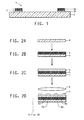
- FIG. 1 is a schematic diagram showing a light-transmitting electromagnetic shield member 1 fabricated in accordance with this invention.
- a photosensitive thick-film electrically conductive paste which contains a conductive powder and a photosensitive resin and a photosensitive thick-film black paste which contains a black pigment and a photosensitive resin are applied by screen printing onto the surface of a glass substrate 2.
- the places where an electromagnetic shield pattern having a predetermined geometric pattern are to remain are exposed to UV light through a photomask and developed, following which they are fired in a horizontal profile furnace or a horizontal half-tempering furnace to form an electromagnetic shield pattern 3 having a black layer 3a and 3b [sic].
- the ratio St/Ss between the total surface area St of the unexposed regions and the total surface area Ss of the regions where the light-transmitting electromagnetic shield has been formed is at least 1 but not more than 99, the linewidth Ws is from 1 to 50 ⁇ m, the film thickness T is from 0.1 to 50 ⁇ m, and the shield is integrally formed with the substrate glass.
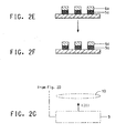
- the method of forming a light-transmitting electromagnetic shield according to one embodiment of the invention is described below while referring to FIG. 2. This method includes the following sequence of steps.
- the black composition used in the invention contains RuO 2 and/or ruthenium polynary oxides. These conductive particles may optionally contain precious metals which include gold, silver, platinum, palladium, copper or combinations thereof which are described below in section (B).
- Ruthenium polynary oxides are one type of pyrochlore, which is a polynary compound of Ru +4 , Ir +4 or mixtures (M") thereof having the following general formula: (M x Bi 2-x )(M' y M" 2-y )O 7-z
- M is selected from the group consisting of yttrium, thallium, indium, cadmium, lead, copper and rare-earth compounds
- M' is selected from the group consisting of platinum, titanium, chromium, rhodium and antimony
- M" is selected from the group consisting of ruthenium, iridium and mixtures thereof; the letter x is from 0 to 2, but is less than or equal to 1 ( ⁇ 1 ) for mono
- ruthenium-based pyrochlore oxides are described in detail in U.S. Patent No. 3,583,931.
- Preferred ruthenium polynary oxides include ruthenium bismuth oxide Bi 2 Ru 2 O 7 , ruthenium lead oxide Pb 2 Ru 2 O 6 , Pb 1.5 -BiO 0.5 -Ru 2 O 6.5 and GdBiRu 2 O 6 . These substances are readily available in purified form, are not adversely affected by glass binders, are stable even when heated in air to about 1,000°C, and are relatively stable even in a reducing atmosphere.
- the ruthenium oxide and/or ruthenium-based pyrochlore oxides are used in a proportion, based on the weight of the overall composition, including organic medium, of 4 to 50 wt %, preferably 6 to 30 wt %, more preferably 5 to 15 wt %, and most preferably 9 to 12 wt %.
- An electrically conductive metal may, if necessary, be added to the black composition.
- Metal powder of substantially any form, including spherical particles and flakes (of rod-like, conical or tabular shape), may be used to work the invention.
- Preferred metal powders include gold, silver, palladium, platinum, copper and combinations thereof.
- the powder is preferably spherical.
- the metal particle-dispersing liquid must not contain a significant amount of solids having a particle size of less than 0.2 ⁇ m. In cases where the film or layer of organic medium is fired to remove the organic medium and carry out sintering of the inorganic binder and the metal solids, the presence of such tiny particles makes complete combustion of the organic medium difficult.
- the maximum particle size should not exceed the screen thickness. It is preferable for at least 80 wt % of the electrically conductive solids to fall within a range of 0.5 to 10 ⁇ m.
- the surface area/weight ratio of the conductive particles it is preferable for the surface area/weight ratio of the conductive particles to not exceed 20 m 2 /g, preferably 10 m 2 /g, and most preferably 5 m 2 /g. If metal particles having a surface area/weight ratio that exceeds 20 m 2 /g are employed, this adversely affects the sintering properties of both inorganic binders used. Thorough combustion of the organic medium is difficult, and blisters appear.
- Copper oxide is often added to the conductive particles to improve adhesion.
- the copper oxide should be used in the form of finely milled particles, preferably having a size of about 0.5 to 5 microns.
- the copper oxide is used in an amount, based on the overall composition, of about 0.1 to 3 wt %, and preferably about 0.1 to 1.0 wt %. Some or all of the Cu 2 O may be substituted with equimolar CuO.
- the inorganic binders such as glass or frit used in the invention serve to promote sintering of the conductive component particles.
- Use may be made of inorganic binders of any composition known to the art to which the invention relates that have a softening point lower than the melting point of the conductive component.
- the softening point of the inorganic binder exerts a large influence on the sintering temperature.
- the electrically conductive composition in the present invention have a glass softening point of about 325 to 700°C, preferably about 350 to 650°C, and most preferably about 375 to 600°C.
- the most preferred glass frit is a borosilicate frit in combination with salts of lead, bismuth, cadmium, barium, calcium or other alkaline earth metals.
- Methods of preparing such glass flits are well-known in the field to which the invention relates.
- the glass components are melted together as the oxides of the respective components, and the molten composition is poured into water to obtain the frit.
- the components used in the batch may be any compounds which form the desired oxides under ordinary frit production conditions.
- the boron oxide can be obtained from boric acid
- silicon dioxide can be obtained from flint
- barium oxide can be obtained from barium carbonate.
- the solid composition must not agglomerate, and so the frit is passed through a fine screen to remove large particles.
- the inorganic binder must be set to a surface area/weight ratio of 10 m 2 /g or less. It is preferable for at least 90 wt % of the particles to have a particle size of from 0.4 to 10 ⁇ m.
- the inorganic binder it is preferable for the inorganic binder to account for 0.01 to 25 wt % of the conductive or dielectric particles. Too large a proportion of inorganic binder may weaken the ability to bond to the substrate.
- the polymeric binder is important to the composition of the invention.
- the polymeric binder should be selected after taking into account the aqueous developability; a polymeric binder having a high resolution must be selected.
- the following binders are known to satisfy these conditions. These binders are copolymers or interpolymers prepared from (1) non-acidic comonomers containing C 1-10 alkyl acrylates, C 1-10 alkyl methacrylate, styrene, substituted styrene or combinations thereof, and (2) acidic comonomers having ethylenically unsaturated carboxylic acid-containing portions which represent at least 15 wt % of the total polymer weight.
- the presence of acidic comonomer components in the composition is important to the present art.
- the acidic functional groups enable the composition to be developed in an aqueous base such as a 0.8% aqueous solution of sodium carbonate. If the acidic comonomer is present in a concentration of less than 15%, the composition cannot be completely washed away with an aqueous base. When the acidic comonomer is present in a concentration that exceeds 30%, the composition has a low stability under the development conditions, so that only partial development occurs in the pattern-forming areas.
- Suitable acidic comonomers include ethylenically unsaturated monocarboxylic acids such as acrylic acid, methacrylic acid and crotonic acid; ethylenically unsaturated dicarboxylic acids such as fumaric acid, itaconic acid, citraconic acid, vinylsuccinic acid and maleic acid, as well as hemiesters thereof and also, in some cases, anhydrides thereof, and mixtures of any of the above. Because they can be burned more cleanly in a low oxygen atmosphere, methacrylic polymers are preferable to acrylic polymers.
- non-acidic comonomers are the above-described alkyl acrylates or alkyl methacrylates, it is advantageous for these non-acidic comonomers to make up preferably at least 50 wt %, and most preferably 70 to 75 wt %, of the polymeric binder.
- the non-acidic comonomer is styrene or a substituted styrene
- the non-acidic comonomer is preferably 50 wt % composed of polymeric binder, with the remaining 50 wt % being acid anhydrides such as the hemiester of maleic anhydride.
- An example of a preferred substituted styrene is ⁇ -methylstyrene.
- the non-acidic portion of the polymeric binder can include up to about 50 wt % of other non-acidic comonomers in place of the alkyl acrylate, alkyl methacrylate, styrene and substituted styrene portions of the polymer.
- Illustrative examples include acrylonitrile, vinyl acetate and acrylamide.
- such monomers are preferably used in an amount of less than about 25 wt % of the overall polymeric binder.
- the use of a single copolymer or a combination of copolymers as the binder is acceptable so long as each of the above conditions is satisfied.
- polystyrene resin a small amount of other polymeric binders can also be used.
- examples include polyolefins such as polyethylene, polypropylene, polybutylene, polyisoprene and ethylene-propylene copolymers, as well as polyethers which are lower alkylene oxide polymers such as polyethylene oxide.
- These polymers can be prepared by liquid polymerization techniques that are commonly used in the field of acrylate polymerization.
- an acidic acrylate polymer such as that described above is prepared by mixing an ⁇ - or ⁇ -ethylenically unsaturated acid (acidic comonomer) in a relatively low-boiling (75 to 150°C) organic medium together with one or more type of copolymerizable vinyl monomer (non-acidic comonomer) to form a 10 to 60% monomer mixture solution. Polymerization is then carried out by adding a polymerization catalyst to the resulting monomer. The resulting mixture is subsequently heated to the refluxing temperature of the solvent at the ambient pressure. Once the polymerization reaction is substantially complete, the acidic polymer solution that has formed is cooled to room temperature, a sample is collected, and the viscosity, molecular weight and acid equivalence of the polymer are measured.
- the above-described acid-containing polymeric binder must be held to a molecular weight of less than 50,000, preferably less than 25,000, and most preferably less than 15,000.
- the glass transition temperature (Tg) of the polymeric binder In cases where the above composition is applied by screen printing, it is advantageous for the glass transition temperature (Tg) of the polymeric binder to exceed 90°C.
- the above paste is generally dried at a temperature of up to 90°C. If the Tg value of the polymer binder is lower than this temperature, the composition generally has a very high adhesive properties. Substances having a lower Tg value can be employed when the composition is applied by a means other than screen printing.
- the organic polymeric binder generally is present in an amount of 5 to 45 wt %, based on the overall amount of the dried photopolymerizable layer.
- Preferred photoinitiators are those which, when exposed to actinic radiation at a temperature of up to 185°C, are thermally inert but generate free radicals.
- These photoinitiators include substituted or unsubstituted polynuclear quinones, which are compounds having two intramolecular rings within a covalent carbon ring system.
- Illustrative examples include 9,10-anthraquinone, 2-methylanthraquinone, 2-t-butylanthraquinone, octamethylanthraquinone, 1,4-naphthoquinone, 9,10-phenanthrenequinone, benzo[1]anthracen-7,12-dione, 2,3-naphthacen-5,12-dione, 2-methyl-1,4-naphthoquinone, 1,4-dimethylanthraquinone, 2,3-dimethylanthraquinone, 2-phenylanthraquinone, 2,3-diphenylanthraquinone, retenequinone, 7,8,9,10-tetrahydronaphthacen-5,12-dione and 1,2,3,4-tetrahydrobenzo[a]anthracen-7,12-dione.
- photoinitiators include those mentioned in U.S. Patent No. 2,760,863 (of which several are thermally active even at a low temperature such as 85°C, vicinal ketoaldonyl alcohols such as benzoin and pivaloin; acyloin ethers such as the methyl and ethyl ethers of benzoin; and hydrocarbon-substituted aromatic acyloins such as ⁇ -methylbenzoin, ⁇ -allylbenzoin, ⁇ -phenylbenzoin, thioxanthone and its derivatives, and hydrogen donor-containing hydrocarbon-substituted aromatic acyloins.
- Initiators that may be used include photoreducible dyes and reducing agents. These include initiators mentioned in U.S. Patent Nos. 2,850,445, 2,875,047, 3,097,96 [sic], 3,074,974, 3,097,097 and 3,145,104; phenazines, oxazines and quinones, such as Michler's ketone, ethyl Michler's ketone and benzophenone, dimers of leuco dye-containing hydrogen donors with 2,4,5-triphenylimidazolyl compounds, and mixtures of the above (mentioned in U.S. Patent Nos. 3,427,161, 3,479,185 and 3,549,367.
- the sensitizers mentioned in U.S. patent No. 4,162,162 are useful together with photoinitiators and photoinhibitors.
- the photoinitiator or photoinitiator system is included in an amount of 0.05 to 10 wt %, based on the total weight of the dried photopolymerizable layer.
- the photocurable monomer components used in this invention include at least one type of addition polymerizable ethylenically unsaturated compound having at least one polymerizable ethylene group.
- This type of compound can initiate polymer formation by the presence of free radicals, enabling chain extension addition polymerization.
- This monomer compound is non-gaseous, has a boiling point higher than 100°C, and has the effect of imparting plasticity to the organic polymeric binder.
- Monomers which can be used alone or in combination with other monomers include t-butyl (meth)acrylate, 1,5-pentanediol di(meth)acrylate, N,N-dimethylaminoethyl (meth)acrylate, ethylene glycol di(meth)acrylate, 1,4-butanediol di(meth)acrylate, diethylene glycol di(meth)acrylate, hexamethylene glycol di(meth)acrylate, 1,3-propanediol di(meth)acrylate, hexamethylene glycol di(meth)acrylate, 1,4-cyclohexanediol di(meth)acrylate, 2,2-dimethylolpropane di(meth)acrylate, glycerol di(meth)acrylate, tripropylene glycol di(meth)acrylate, glycerol tri(meth)acrylate, trimethylol propane tri(meth)acrylate, the compounds mentioned in U
- Patent No. 3,380,381 2,2-di(p-hydroxyphenyl)propane di(meth)acrylate, pentaerythritol tetra(meth)acrylate, triethylene glycol diacrylate, polyoxethyl-1,2-di-(p-hydroxyethyl)propane dimethacrylate, bisphenyl A di-[3-(meth)acryloxy-2-hydroxypropyl) ether, bisphenol A di-[2-(meth)acryloxyethyl)ether, 1,4-butanedioldi-(3-methacryloxy-2-hydroxypropyl) ether, triethylene glycol dimethacrylate, polyoxypropyltrimethylolpropane triacrylate, butylene glycol di(meth)acrylate, 1,2,4-butanediol tri(meth)acrylate, 2,2,4-trimethyl-1,3-pentanediol di(meth)acrylate, 1-phenylethylene-1
- Useful examples include ethylenically unsaturated compounds having a molecular weight of at least 300, such as alkylene glycols or polyalkylene glycols which are C 2-15 alkylene glycols having 1 to 10 ether bonds; and alkylene or polyalkylene glycol diacrylates mentioned in U.S. Patent No. 2,927,022, such as those which, particularly when present as the end group, are prepared from addition polymerizable ethylene bond-bearing compounds.
- Preferred monomers are polyoxyethylated trimethylolpropane tri(meth)acrylate, ethylated pentaerythritol triacrylate, trimethylolpropane tri(meth)acrylate, dipentaerythritol monohydroxypentaacrylate and 1,10-decanediol dimethacrylate.
- Other preferred monomers include monohydroxypolycaprolactone monoacrylate, polyethylene glycol diacrylate (molecular weight, about 200) and polyethylene glycol dimethacrylate (molecular weight, about 400).
- the unsaturated monomer component is included in an amount of 1 to 20 wt %, based on the total weight of the dried photopolymerizable layer.
- the main purpose for using an organic medium is to have it function as a medium which is capable of rendering a liquid dispersion of finely milled solids of the above-described composition into a form that can easily be applied onto a ceramic or other type of substrate. Accordingly, the organic medium must first be a substance capable of dispersing the solids while maintaining a suitable degree of stability. Secondly, the rheological properties of the organic medium must confer good coating properties to the liquid dispersion.
- the solvent component (which may be a solvent mixture) selected is one in which the polymer and other organic components completely dissolve.
- a solvent which is inert to (non-reactive with) the paste composition and other components must be selected.
- the solvent selected must be one which has a sufficiently high volatility and which can evaporate from a liquid dispersion even when applied at atmospheric pressure and a relatively low temperature. However, it must not have such a degree of volatility that the paste on the screen dries rapidly at normal room temperature during the printing step.
- Solvents preferable for use in the paste composition are those which have a boiling point at ambient pressure of less than 300°C, and preferably less than 250°C.
- solvents include aliphatic alcohols; esters of such alcohols, such as the acetic acid ester or propionic acid ester; terpenes such as rosin, ⁇ - or ⁇ -terpineol, and mixtures thereof; ethylene glycol esters such as ethylene glycol, ethylene glycol monobutyl ether and butyl cellosolve acetate; carbitol esters such as butyl carbitol, butyl carbitol acetate and carbitol acetate; and other suitable solvents such as Texanol (2,2,4-trimethyl-1 ,3-pentanediol monoisobutyrate).
- Such additional components known in the art to which the invention relates as dispersants, stabilizers, plasticizers, release agents, dispersants [sic], stripping agents, anti-foaming agents and wetting agents may also be included in the composition.
- dispersants such as dispersants, stabilizers, plasticizers, release agents, dispersants [sic], stripping agents, anti-foaming agents and wetting agents.
- the metal electrically conductive composition (in paste or sheet form) used in this invention is a commercial photosensitive thick-film conductor composition.
- Preferred compositions for use in this invention include silver powder, UV-polymerizable carrier and glass frit.
- the conductor phase is a main component of the composition. It is composed of silver particles having a particle size within a range of 0.05 to 20 ⁇ m and having a shape which may be random or in the form of flakes. In cases where a UV-polymerizable medium is used together with the composition, it is preferable for the silver particles to have a size within a range of 0.3 to 10 ⁇ m. Preferred compositions contain the silver particles in a proportion of 66 wt %, based on the combined amount of all the components in the thick-film paste. In this case, the surface area of the silver particles is 0.34 m 2 /g.
- the metal conductive composition contains, as finely milled inorganic particles, from 1 to 10 wt % of a refractory substance that does not form a glass, or a precursor thereof.
- a refractory substance that does not form a glass, or a precursor thereof.
- Illustrative examples include aluminum oxide, copper oxide, cadmium oxide, gadolinium oxide, zirconium oxide, cobalt oxide/iron/chromium, aluminum and copper.
- These oxides or oxide precursors have a particle size within a range of 0.05 to 44 ⁇ m, and at least 80 wt % of the particles have a size within a range of 0.1 to 5 ⁇ m.
- This composition contains 5 to 20 wt % of glass frit having a softening point within a range of 325 to 600°C.
- Preferred glass frits are borosilicate-lead glasses.
- the following composition is especially preferred: PbO (53.1), B 2 O 3 (2.9), SiO 2 (29.0), TiO 2 (3.0), ZrO 2 (3.0), ZnO (2.0), Na 2 O (3.0) and CdO (4.0).
- Such a glass frit and suitable additives are formulated so that, when fine lines of fired metal oxides are immersed for one hour in a molten coating agent at 600°C, neither reaction nor dissolution will occur, failure will not take place and adhesion to the underlying black electrode will remain intact.
- the metal conductive composition may additionally include 10 to 30 wt % of a photosensitive medium in which the above-described granular substances are dispersed.
- a photosensitive medium is a solution of methyl polymethacrylate and a polyfunctional monomer. This monomer should be one having a low volatility in order to minimize volatilization during preparation of the silver conductor composition paste and during the printing/drying steps prior to carrying out UV curing.
- the photosensitive medium includes also a solvent and a UV-sensitive initiator.
- Preferred UV-polymerizable media include polymers based on methyl methacrylate/ethyl acrylate in a weight ratio of 95:5.
- the above-described silver conductor composition is formulated as a free-flowing paste having a viscosity of 50 to 200 Pa ⁇ s.
- Non-limiting examples of suitable solvents for the above-described medium include butyl carbitol acetate and ⁇ -terpineol. These solvents can additionally include, for example, dispersants and stabilizers.
- This metal conductive composition may have applied thereon a coating agent composition containing 85 parts of glass frit (composition (mol %): PbO, 68.2; SiO 2 , 12.0; B 2 O 3 , 14.1; CdO, 5.7; softening point, 480) and 14 parts of ethyl cellulose carrier.
- the resulting coated electrode assembly is useful for the fabrication of AC plasma display panels.
- FODEL® silver paste made by DuPont was used as the photosensitive thick-film electrically conductive paste
- FODEL® ruthenium oxide paste made by DuPont was used as the photosensitive thick-film black paste
- soda lime glass having a thickness of 2.5 to 3 mm was used as the glass substrate. To achieve a good visibility, the glass substrate was required to be one of good quality, without defects such as internal air bubbles and surface scratches.
- the FODEL® ruthenium oxide paste (made by DuPont) used as the photosensitive thick-film black paste was screen-printed onto a 2x3 inch glass substrate (high-yield point glass PD200, made by Asahi Glass Co., Ltd.) using a 380 mesh polyester screen and dried in a batch-type hot air drying furnace at a peak temperature of 80°C and a total 20-minute profile to form a dry film of the photosensitive thick-film black paste FODEL® DC246 (DuPont).
- the photosensitive thick-film silver paste FODEL® silver paste (made by DuPont) was lamination coated by a screen printing process using a 350 calender mesh polyester screen onto the dry film of photosensitive thick-film black paste that had been formed on the glass substrate, then fired in a batch hot-air drying furnace at a peak temperature of 80°C and a total 20-minute profile, thereby forming a dry film composed of two layers: the dried photosensitive thick-film black paste FODEL® ruthenium oxide (made by DuPont) and the photosensitive thick-film silver paste FODEL® silver paste (made by DuPont).
- the high yield point glass PD200 made by Asahi Glass was used as the glass substrate in this case, any soda lime glass generally available on the market may be used.
- the dry film composed of two layers was exposed, through a photomask bearing a geometric pattern corresponding to a shield pattern, in regions where the shield pattern was to be formed, thereby defined the irradiated region as a shield pattern.
- the exposed substrate was subsequently shower developed with 0.4% aqueous sodium carbonate using a planar developing machine and the unexposed areas of the two-layer dry film were removed, thereby giving a dry film composed of the above-described two layers in a shield pattern.
- the glass substrate on which the above two-layer dry film was formed in the above-described shield pattern was then air-dried in a horizontal near-infrared firing furnace at a peak temperature of 700°C for a total of 7 minutes so as to sinter the two layers and fix them to the glass substrate, thereby yielding the desired light-transmitting electromagnetic shield member.
- Table 1 shows the results obtained from examining the appearance after firing in each of Examples 1 to 4 according to the invention, as well as the resolution (linewidth and line pitch), exposure energy and conditions during development in each case.
- the development time is defined here as the "time to clear” (TTC); that is, the time required for development of all the unexposed dry material.
- TTC time to clear
- the development time in Table 1 is given as a ratio with respect to the TTC.
- Example 4 the surface resistivity (measured with a four-probe resistivity meter), aperture ratio (measured using a contact-type measuring instrument manufactured by Tokyo Seimitsu Co., Ltd.) and the visible light transmittance were measured.
- the visible light transmittance the value for just the electromagnetic shield without the glass substrate was used for the sake of comparison.
- the numerical value for the visible light transmittance coincides with the aperture ratio.
- Table 2 The results are shown in Table 2 together with the results obtained in the comparative examples.
- a commercially available electromagnetic shield mesh for use as a front filter in plasma display panels (made by Nippon Filcon Co., Ltd.) was used as a control for the sake of comparison.
- the numerical values were taken from the company's product catalog. This company has a market share in the PDP front filter market of at least two-thirds, and was judged to be the most suitable as a control for comparison with the present invention.
- the surface resistivity required to conform to the U.S. Federal Communication Commission's Class B standards (i.e., 1.5 ⁇ / ⁇ or less) was shown as a comparative value. Yet, as is apparent from the catalog value for the electromagnetic shield mesh made by Nippon Filcon Co., Ltd., in the market, a value of 0.1 ⁇ / ⁇ or less is in fact required. The latter was thus regarded as the value actually demanded for practical purposes.
- the present invention provides photosensitive electrically conductive paste materials for forming light-transmitting electromagnet shields which have a sufficient electromagnetic shielding effect, excellent light-transmitting properties, non-visibility and viewing angle; possess sufficient durability while maintaining outside light reflection-suppressing effects; are able to reduce the number of steps compared with the prior art; allow the effective reuse of precious metals such as silver by recycling, thereby helping to hold down production costs; and at the same time are very environmentally friendly.
- This invention also provides light-transmitting electromagnetic shields formed from such paste materials, and a method of fabricating such shields.
Landscapes
- Chemical & Material Sciences (AREA)
- Engineering & Computer Science (AREA)
- Life Sciences & Earth Sciences (AREA)
- Chemical Kinetics & Catalysis (AREA)
- General Chemical & Material Sciences (AREA)
- Geochemistry & Mineralogy (AREA)
- Materials Engineering (AREA)
- Organic Chemistry (AREA)
- Physics & Mathematics (AREA)
- General Physics & Mathematics (AREA)
- Microelectronics & Electronic Packaging (AREA)
- Manufacturing & Machinery (AREA)
- Ceramic Engineering (AREA)
- Electromagnetism (AREA)
- Plasma & Fusion (AREA)
- Inorganic Chemistry (AREA)
- Dispersion Chemistry (AREA)
- Spectroscopy & Molecular Physics (AREA)
- Shielding Devices Or Components To Electric Or Magnetic Fields (AREA)
- Laminated Bodies (AREA)
- Devices For Indicating Variable Information By Combining Individual Elements (AREA)
- Materials For Photolithography (AREA)
- Paints Or Removers (AREA)
Applications Claiming Priority (4)
| Application Number | Priority Date | Filing Date | Title |
|---|---|---|---|
| US49565703P | 2003-08-15 | 2003-08-15 | |
| US495657P | 2003-08-15 | ||
| US891925 | 2004-07-15 | ||
| US10/891,925 US20050037278A1 (en) | 2003-08-15 | 2004-07-15 | Photosensitive thick-film paste materials for forming light-transmitting electromagnetic shields, light-transmitting electromagnetic shields formed using the same, and method of manufacture thereof |
Publications (1)
| Publication Number | Publication Date |
|---|---|
| EP1507169A1 true EP1507169A1 (de) | 2005-02-16 |
Family
ID=33567985
Family Applications (1)
| Application Number | Title | Priority Date | Filing Date |
|---|---|---|---|
| EP04018685A Withdrawn EP1507169A1 (de) | 2003-08-15 | 2004-08-06 | Lichtempfindliche Dickschichtmaterialien in Pastenform zur Herstellung lichtdurchlässiger elektromagnetischer Abschirmungen, daraus hergestellte lichtdurchlässige elektromagnetische Abschirmungen und Verfahren zu deren Herstellung |
Country Status (6)
| Country | Link |
|---|---|
| US (1) | US20050037278A1 (de) |
| EP (1) | EP1507169A1 (de) |
| JP (1) | JP2005173551A (de) |
| KR (1) | KR100719016B1 (de) |
| CN (1) | CN1620245A (de) |
| TW (1) | TW200532370A (de) |
Cited By (1)
| Publication number | Priority date | Publication date | Assignee | Title |
|---|---|---|---|---|
| CN101030038B (zh) * | 2006-03-03 | 2012-07-04 | E.I.内穆尔杜邦公司 | 聚合物溶液、可水性显影的厚膜组合物、其制法及由其形成的电极 |
Families Citing this family (25)
| Publication number | Priority date | Publication date | Assignee | Title |
|---|---|---|---|---|
| US7153620B2 (en) * | 2003-09-23 | 2006-12-26 | Eastman Kodak Company | Transparent invisible conductive grid |
| JP4760709B2 (ja) * | 2004-07-22 | 2011-08-31 | 東レ株式会社 | 感光性ペーストおよびディスプレイパネル用部材の製造方法 |
| JP4837297B2 (ja) * | 2005-03-09 | 2011-12-14 | 富士フイルム株式会社 | 遮光画像付き基板及び遮光画像の形成方法、転写材料、カラーフィルター、並びに表示装置 |
| US20060223690A1 (en) * | 2005-04-01 | 2006-10-05 | Tsutomu Mutoh | Photosensitive thick-film dielectric paste composition and method for making an insulating layer using same |
| US20070001566A1 (en) * | 2005-06-30 | 2007-01-04 | D Haene Pol | Impact resistant, direct contact plasma display panel filters |
| US20110083874A1 (en) * | 2009-10-09 | 2011-04-14 | E. I. Du Pont De Nemours And Company | Electrode and method for manufacturing the same |
| US20070212510A1 (en) * | 2006-03-13 | 2007-09-13 | Henry Hieslmair | Thin silicon or germanium sheets and photovoltaics formed from thin sheets |
| KR100787450B1 (ko) * | 2006-06-20 | 2007-12-26 | 삼성에스디아이 주식회사 | 감광성 페이스트 조성물 이를 이용하여 제조된 플라즈마디스플레이 패널의 격벽 및 이를 포함하는 플라즈마디스플레이 패널 |
| US7608784B2 (en) * | 2006-07-13 | 2009-10-27 | E. I. Du Pont De Nemours And Company | Photosensitive conductive paste for electrode formation and electrode |
| KR100852706B1 (ko) * | 2007-03-02 | 2008-08-19 | 삼성에스디아이 주식회사 | 격벽 형성용 조성물, 및 이를 이용하여 제조된 플라즈마디스플레이 패널 |
| KR100894062B1 (ko) * | 2007-03-26 | 2009-04-21 | 삼성에스디아이 주식회사 | 감광성 페이스트 조성물, 이를 이용하여 제조된 플라즈마디스플레이 패널의 격벽 및 이를 포함하는 플라즈마디스플레이 패널 |
| US7648655B2 (en) * | 2007-10-30 | 2010-01-19 | E. I. Du Pont De Nemours And Company | Conductive composition for black bus electrode, and front panel of plasma display panel |
| JP2011018636A (ja) * | 2009-06-09 | 2011-01-27 | Fujifilm Corp | 導電性組成物、並びに透明導電膜、表示素子及び集積型太陽電池 |
| WO2011114335A1 (en) * | 2010-03-17 | 2011-09-22 | Hanita Coatings R.C.A. Ltd | Polymeric substrate with laminated glass layer |
| US9434644B2 (en) | 2010-09-30 | 2016-09-06 | Avanstrate Inc. | Cover glass and method for producing cover glass |
| SG190520A1 (en) * | 2011-11-09 | 2013-06-28 | Heraeus Precious Metals Gmbh | Thick film conductive composition and use thereof |
| KR101321368B1 (ko) * | 2011-12-20 | 2013-10-28 | 금호석유화학 주식회사 | 도전성 복합 미립자 및 이를 포함하는 도전성 페이스트 조성물 |
| CN103646672A (zh) * | 2013-12-02 | 2014-03-19 | 朱嵘飞 | 一种集材料与结构吸波功能于一体的新型吸波功能设计 |
| CN105960683A (zh) * | 2014-02-12 | 2016-09-21 | 东丽株式会社 | 导电糊剂、图案的制造方法、导电图案的制造方法和传感器 |
| JP6777486B2 (ja) * | 2015-09-25 | 2020-10-28 | 三星電子株式会社Samsung Electronics Co.,Ltd. | 導電体、その製造方法、およびこれを含む素子 |
| CN105537581B (zh) * | 2016-01-11 | 2018-06-26 | 横店集团东磁股份有限公司 | 一种噪音抑制片及其制备方法 |
| CN106292102A (zh) * | 2016-08-12 | 2017-01-04 | 京东方科技集团股份有限公司 | 一种显示面板及显示器 |
| KR101828822B1 (ko) * | 2017-01-19 | 2018-02-13 | 주식회사 지앤아이솔루션 | 광학 렌즈 제조 장치 |
| KR101810815B1 (ko) * | 2017-04-07 | 2017-12-20 | 김병삼 | 마이크로 크랙 및 레이저 타공홀을 포함하는 전파투과성 센서 커버의 제조 방법 및 이를 이용하여 제조된 전파투과성 센서 커버 |
| TWI836264B (zh) * | 2020-09-04 | 2024-03-21 | 日商旭化成股份有限公司 | 金屬配線的製造方法及套組 |
Citations (6)
| Publication number | Priority date | Publication date | Assignee | Title |
|---|---|---|---|---|
| EP0863534A2 (de) * | 1997-03-06 | 1998-09-09 | E.I. Du Pont De Nemours And Company | Plasma Anzeigetafel und Herstellungsverfahren derselben |
| US6120975A (en) * | 1997-11-04 | 2000-09-19 | Taiyo Ink Manufacturing Co., Ltd. | Methods for production of a plasma display panel |
| US6156433A (en) * | 1996-01-26 | 2000-12-05 | Dai Nippon Printing Co., Ltd. | Electrode for plasma display panel and process for producing the same |
| EP1239717A2 (de) * | 2001-03-08 | 2002-09-11 | Sumitomo Chemical Company Limited | Platte zur elektromagnetischen Abschirmung und deren Herstellungsverfahren |
| US20030013048A1 (en) * | 2001-07-13 | 2003-01-16 | Shielding Express, Inc. | Electromagnetic filter for display screens |
| US20030044582A1 (en) * | 2001-08-28 | 2003-03-06 | Sakoske George Emil | Screen printing process |
Family Cites Families (18)
| Publication number | Priority date | Publication date | Assignee | Title |
|---|---|---|---|---|
| NL87862C (de) * | 1951-08-20 | |||
| US2850445A (en) * | 1955-01-19 | 1958-09-02 | Oster Gerald | Photopolymerization |
| US2875047A (en) * | 1955-01-19 | 1959-02-24 | Oster Gerald | Photopolymerization with the formation of coherent plastic masses |
| NL218803A (de) * | 1956-07-09 | |||
| US3074974A (en) * | 1957-12-06 | 1963-01-22 | Monsanto Chemicals | Method for the preparation of diglycidyl ether of tetrachlorobisphenol-a |
| US3097097A (en) * | 1959-02-12 | 1963-07-09 | Gisela K Oster | Photo degrading of gel systems and photographic production of reliefs therewith |
| US3154104A (en) * | 1962-12-17 | 1964-10-27 | Honeywell Inc | Rolling gate valve |
| GB1090142A (en) * | 1965-02-26 | 1967-11-08 | Agfa Gevaert Nv | Photochemical insolubilisation of polymers |
| US3479185A (en) * | 1965-06-03 | 1969-11-18 | Du Pont | Photopolymerizable compositions and layers containing 2,4,5-triphenylimidazoyl dimers |
| US3380381A (en) * | 1965-08-06 | 1968-04-30 | Western Printing Mach Co | Rotary press printing cylinder for clamping flexible plates |
| US3549367A (en) * | 1968-05-24 | 1970-12-22 | Du Pont | Photopolymerizable compositions containing triarylimidazolyl dimers and p-aminophenyl ketones |
| US3583931A (en) * | 1969-11-26 | 1971-06-08 | Du Pont | Oxides of cubic crystal structure containing bismuth and at least one of ruthenium and iridium |
| US4162162A (en) * | 1978-05-08 | 1979-07-24 | E. I. Du Pont De Nemours And Company | Derivatives of aryl ketones and p-dialkyl-aminoarylaldehydes as visible sensitizers of photopolymerizable compositions |
| US5032490A (en) * | 1989-08-21 | 1991-07-16 | E. I. Du Pont De Nemours And Company | Photosensitive aqueous developable copper conductor composition |
| JPH0955167A (ja) * | 1995-06-05 | 1997-02-25 | Dainippon Printing Co Ltd | プラズマディスプレイパネル用電極及びその形成方法 |
| GB2304201B (en) * | 1995-08-04 | 1999-04-07 | Sony Corp | Methods of forming a fluorescent screen on the front panel of a cathode ray tube |
| JPH1055758A (ja) * | 1996-06-03 | 1998-02-24 | Dainippon Printing Co Ltd | 厚膜パターン形成方法 |
| US6451088B1 (en) * | 2001-07-25 | 2002-09-17 | Phelps Dodge Corporation | Method for improving metals recovery using high temperature leaching |
-
2004
- 2004-07-15 US US10/891,925 patent/US20050037278A1/en not_active Abandoned
- 2004-08-06 EP EP04018685A patent/EP1507169A1/de not_active Withdrawn
- 2004-08-13 KR KR1020040063968A patent/KR100719016B1/ko not_active Expired - Fee Related
- 2004-08-13 CN CNA200410089970XA patent/CN1620245A/zh active Pending
- 2004-08-13 TW TW093124449A patent/TW200532370A/zh unknown
- 2004-08-13 JP JP2004236027A patent/JP2005173551A/ja active Pending
Patent Citations (6)
| Publication number | Priority date | Publication date | Assignee | Title |
|---|---|---|---|---|
| US6156433A (en) * | 1996-01-26 | 2000-12-05 | Dai Nippon Printing Co., Ltd. | Electrode for plasma display panel and process for producing the same |
| EP0863534A2 (de) * | 1997-03-06 | 1998-09-09 | E.I. Du Pont De Nemours And Company | Plasma Anzeigetafel und Herstellungsverfahren derselben |
| US6120975A (en) * | 1997-11-04 | 2000-09-19 | Taiyo Ink Manufacturing Co., Ltd. | Methods for production of a plasma display panel |
| EP1239717A2 (de) * | 2001-03-08 | 2002-09-11 | Sumitomo Chemical Company Limited | Platte zur elektromagnetischen Abschirmung und deren Herstellungsverfahren |
| US20030013048A1 (en) * | 2001-07-13 | 2003-01-16 | Shielding Express, Inc. | Electromagnetic filter for display screens |
| US20030044582A1 (en) * | 2001-08-28 | 2003-03-06 | Sakoske George Emil | Screen printing process |
Cited By (1)
| Publication number | Priority date | Publication date | Assignee | Title |
|---|---|---|---|---|
| CN101030038B (zh) * | 2006-03-03 | 2012-07-04 | E.I.内穆尔杜邦公司 | 聚合物溶液、可水性显影的厚膜组合物、其制法及由其形成的电极 |
Also Published As
| Publication number | Publication date |
|---|---|
| KR20050019058A (ko) | 2005-02-28 |
| KR100719016B1 (ko) | 2007-05-16 |
| CN1620245A (zh) | 2005-05-25 |
| JP2005173551A (ja) | 2005-06-30 |
| TW200532370A (en) | 2005-10-01 |
| US20050037278A1 (en) | 2005-02-17 |
Similar Documents
| Publication | Publication Date | Title |
|---|---|---|
| US20050037278A1 (en) | Photosensitive thick-film paste materials for forming light-transmitting electromagnetic shields, light-transmitting electromagnetic shields formed using the same, and method of manufacture thereof | |
| JP5080743B2 (ja) | 黒色導電性厚膜組成物、黒色電極、およびこれらの形成方法 | |
| JP3779297B2 (ja) | 光形成性黒色電極および黒色電極組成物 | |
| EP0186114B1 (de) | Photoempfindliche leitfähige metallische Zusammensetzung | |
| US7105256B2 (en) | Photosensitive conductive composition and plasma display panel formed by using the same | |
| JP5654588B2 (ja) | 電極およびその製造方法 | |
| KR20090029305A (ko) | 전극 형성용 감광성 도전 페이스트 및 전극 | |
| US7135267B2 (en) | Aqueous developable photoimageable compositions for use in photo-patterning methods | |
| KR101100490B1 (ko) | 플라즈마 디스플레이 패널용 전극 페이스트 및 플라즈마 디스플레이 패널용 블랙 버스 전극 | |
| US20100093248A1 (en) | Photosensitive conductive paste for electrode formation and electrode | |
| JP4503306B2 (ja) | フィールドエミッション型ディスプレイ装置用の電極形成組成物およびそのような組成物の使用方法 | |
| JP2012513624A (ja) | 感光性ペーストおよびそれを用いたパターン生産方法 | |
| JP5108239B2 (ja) | 黒色導電性組成物、黒色電極、およびその形成方法 | |
| KR100904145B1 (ko) | 흑색 전도성 후막 조성물, 흑색 전극 및 그의 제조 방법 | |
| US20060202174A1 (en) | Black conductive compositions, black electrodes, and methods of forming thereof | |
| US20060223690A1 (en) | Photosensitive thick-film dielectric paste composition and method for making an insulating layer using same | |
| JP2012514309A (ja) | Pdpの前部電極 | |
| KR20060047146A (ko) | 감광성 도체 그린 시트 | |
| JP2004205532A (ja) | 感光性フィルム及びプラズマディスプレイ用2層構造電極の製造方法 |
Legal Events
| Date | Code | Title | Description |
|---|---|---|---|
| PUAI | Public reference made under article 153(3) epc to a published international application that has entered the european phase |
Free format text: ORIGINAL CODE: 0009012 |
|
| AK | Designated contracting states |
Kind code of ref document: A1 Designated state(s): AT BE BG CH CY CZ DE DK EE ES FI FR GB GR HU IE IT LI LU MC NL PL PT RO SE SI SK TR |
|
| AX | Request for extension of the european patent |
Extension state: AL HR LT LV MK |
|
| 17P | Request for examination filed |
Effective date: 20050812 |
|
| AKX | Designation fees paid |
Designated state(s): DE FR GB |
|
| 17Q | First examination report despatched |
Effective date: 20080611 |
|
| STAA | Information on the status of an ep patent application or granted ep patent |
Free format text: STATUS: THE APPLICATION IS DEEMED TO BE WITHDRAWN |
|
| 18D | Application deemed to be withdrawn |
Effective date: 20081223 |