EP1508936A1 - Méthode de fabrication d'un diplexeur avec circuit imprimé encastré et duplexeur fabriqué par cette méthode - Google Patents
Méthode de fabrication d'un diplexeur avec circuit imprimé encastré et duplexeur fabriqué par cette méthode Download PDFInfo
- Publication number
- EP1508936A1 EP1508936A1 EP04253883A EP04253883A EP1508936A1 EP 1508936 A1 EP1508936 A1 EP 1508936A1 EP 04253883 A EP04253883 A EP 04253883A EP 04253883 A EP04253883 A EP 04253883A EP 1508936 A1 EP1508936 A1 EP 1508936A1
- Authority
- EP
- European Patent Office
- Prior art keywords
- filter
- pcb
- duplexer
- filters
- metal layer
- Prior art date
- Legal status (The legal status is an assumption and is not a legal conclusion. Google has not performed a legal analysis and makes no representation as to the accuracy of the status listed.)
- Granted
Links
Images




Classifications
-
- H—ELECTRICITY
- H03—ELECTRONIC CIRCUITRY
- H03H—IMPEDANCE NETWORKS, e.g. RESONANT CIRCUITS; RESONATORS
- H03H9/00—Networks comprising electromechanical or electro-acoustic elements; Electromechanical resonators
- H03H9/70—Multiple-port networks for connecting several sources or loads, working on different frequencies or frequency bands, to a common load or source
- H03H9/703—Networks using bulk acoustic wave devices
- H03H9/706—Duplexers
-
- H—ELECTRICITY
- H01—ELECTRIC ELEMENTS
- H01P—WAVEGUIDES; RESONATORS, LINES, OR OTHER DEVICES OF THE WAVEGUIDE TYPE
- H01P1/00—Auxiliary devices
- H01P1/20—Frequency-selective devices, e.g. filters
- H01P1/201—Filters for transverse electromagnetic waves
- H01P1/205—Comb or interdigital filters; Cascaded coaxial cavities
-
- H—ELECTRICITY
- H01—ELECTRIC ELEMENTS
- H01P—WAVEGUIDES; RESONATORS, LINES, OR OTHER DEVICES OF THE WAVEGUIDE TYPE
- H01P1/00—Auxiliary devices
- H01P1/20—Frequency-selective devices, e.g. filters
- H01P1/213—Frequency-selective devices, e.g. filters combining or separating two or more different frequencies
-
- H—ELECTRICITY
- H03—ELECTRONIC CIRCUITRY
- H03H—IMPEDANCE NETWORKS, e.g. RESONANT CIRCUITS; RESONATORS
- H03H9/00—Networks comprising electromechanical or electro-acoustic elements; Electromechanical resonators
- H03H9/02—Details
- H03H9/05—Holders or supports
- H03H9/0538—Constructional combinations of supports or holders with electromechanical or other electronic elements
- H03H9/0566—Constructional combinations of supports or holders with electromechanical or other electronic elements for duplexers
- H03H9/0571—Constructional combinations of supports or holders with electromechanical or other electronic elements for duplexers including bulk acoustic wave [BAW] devices
-
- H—ELECTRICITY
- H05—ELECTRIC TECHNIQUES NOT OTHERWISE PROVIDED FOR
- H05K—PRINTED CIRCUITS; CASINGS OR CONSTRUCTIONAL DETAILS OF ELECTRIC APPARATUS; MANUFACTURE OF ASSEMBLAGES OF ELECTRICAL COMPONENTS
- H05K1/00—Printed circuits
- H05K1/16—Printed circuits incorporating printed electric components, e.g. printed resistors, capacitors or inductors
- H05K1/165—Printed circuits incorporating printed electric components, e.g. printed resistors, capacitors or inductors incorporating printed inductors
-
- H—ELECTRICITY
- H05—ELECTRIC TECHNIQUES NOT OTHERWISE PROVIDED FOR
- H05K—PRINTED CIRCUITS; CASINGS OR CONSTRUCTIONAL DETAILS OF ELECTRIC APPARATUS; MANUFACTURE OF ASSEMBLAGES OF ELECTRICAL COMPONENTS
- H05K1/00—Printed circuits
- H05K1/02—Details
- H05K1/0213—Electrical arrangements not otherwise provided for
- H05K1/0237—High frequency adaptations
- H05K1/0243—Printed circuits associated with mounted high frequency components
-
- H—ELECTRICITY
- H05—ELECTRIC TECHNIQUES NOT OTHERWISE PROVIDED FOR
- H05K—PRINTED CIRCUITS; CASINGS OR CONSTRUCTIONAL DETAILS OF ELECTRIC APPARATUS; MANUFACTURE OF ASSEMBLAGES OF ELECTRICAL COMPONENTS
- H05K1/00—Printed circuits
- H05K1/16—Printed circuits incorporating printed electric components, e.g. printed resistors, capacitors or inductors
- H05K1/162—Printed circuits incorporating printed electric components, e.g. printed resistors, capacitors or inductors incorporating printed capacitors
-
- H—ELECTRICITY
- H05—ELECTRIC TECHNIQUES NOT OTHERWISE PROVIDED FOR
- H05K—PRINTED CIRCUITS; CASINGS OR CONSTRUCTIONAL DETAILS OF ELECTRIC APPARATUS; MANUFACTURE OF ASSEMBLAGES OF ELECTRICAL COMPONENTS
- H05K2201/00—Indexing scheme relating to printed circuits covered by H05K1/00
- H05K2201/09—Shape and layout
- H05K2201/09209—Shape and layout details of conductors
- H05K2201/095—Conductive through-holes or vias
- H05K2201/0959—Plated through-holes or plated blind vias filled with insulating material
-
- H—ELECTRICITY
- H05—ELECTRIC TECHNIQUES NOT OTHERWISE PROVIDED FOR
- H05K—PRINTED CIRCUITS; CASINGS OR CONSTRUCTIONAL DETAILS OF ELECTRIC APPARATUS; MANUFACTURE OF ASSEMBLAGES OF ELECTRICAL COMPONENTS
- H05K2201/00—Indexing scheme relating to printed circuits covered by H05K1/00
- H05K2201/10—Details of components or other objects attached to or integrated in a printed circuit board
- H05K2201/10007—Types of components
- H05K2201/1006—Non-printed filter
-
- H—ELECTRICITY
- H05—ELECTRIC TECHNIQUES NOT OTHERWISE PROVIDED FOR
- H05K—PRINTED CIRCUITS; CASINGS OR CONSTRUCTIONAL DETAILS OF ELECTRIC APPARATUS; MANUFACTURE OF ASSEMBLAGES OF ELECTRICAL COMPONENTS
- H05K3/00—Apparatus or processes for manufacturing printed circuits
- H05K3/40—Forming printed elements for providing electric connections to or between printed circuits
- H05K3/42—Plated through-holes or plated via connections
- H05K3/429—Plated through-holes specially for multilayer circuits, e.g. having connections to inner circuit layers
-
- H—ELECTRICITY
- H05—ELECTRIC TECHNIQUES NOT OTHERWISE PROVIDED FOR
- H05K—PRINTED CIRCUITS; CASINGS OR CONSTRUCTIONAL DETAILS OF ELECTRIC APPARATUS; MANUFACTURE OF ASSEMBLAGES OF ELECTRICAL COMPONENTS
- H05K3/00—Apparatus or processes for manufacturing printed circuits
- H05K3/46—Manufacturing multilayer circuits
- H05K3/4644—Manufacturing multilayer circuits by building the multilayer layer by layer, i.e. build-up multilayer circuits
- H05K3/4652—Adding a circuit layer by laminating a metal foil or a preformed metal foil pattern
-
- H—ELECTRICITY
- H10—SEMICONDUCTOR DEVICES; ELECTRIC SOLID-STATE DEVICES NOT OTHERWISE PROVIDED FOR
- H10W—GENERIC PACKAGES, INTERCONNECTIONS, CONNECTORS OR OTHER CONSTRUCTIONAL DETAILS OF DEVICES COVERED BY CLASS H10
- H10W72/00—Interconnections or connectors in packages
- H10W72/071—Connecting or disconnecting
- H10W72/072—Connecting or disconnecting of bump connectors
-
- H—ELECTRICITY
- H10—SEMICONDUCTOR DEVICES; ELECTRIC SOLID-STATE DEVICES NOT OTHERWISE PROVIDED FOR
- H10W—GENERIC PACKAGES, INTERCONNECTIONS, CONNECTORS OR OTHER CONSTRUCTIONAL DETAILS OF DEVICES COVERED BY CLASS H10
- H10W72/00—Interconnections or connectors in packages
- H10W72/20—Bump connectors, e.g. solder bumps or copper pillars; Dummy bumps; Thermal bumps
- H10W72/241—Dispositions, e.g. layouts
-
- H—ELECTRICITY
- H10—SEMICONDUCTOR DEVICES; ELECTRIC SOLID-STATE DEVICES NOT OTHERWISE PROVIDED FOR
- H10W—GENERIC PACKAGES, INTERCONNECTIONS, CONNECTORS OR OTHER CONSTRUCTIONAL DETAILS OF DEVICES COVERED BY CLASS H10
- H10W90/00—Package configurations
- H10W90/701—Package configurations characterised by the relative positions of pads or connectors relative to package parts
- H10W90/721—Package configurations characterised by the relative positions of pads or connectors relative to package parts of bump connectors
- H10W90/724—Package configurations characterised by the relative positions of pads or connectors relative to package parts of bump connectors between a chip and a stacked insulating package substrate, interposer or RDL
-
- Y—GENERAL TAGGING OF NEW TECHNOLOGICAL DEVELOPMENTS; GENERAL TAGGING OF CROSS-SECTIONAL TECHNOLOGIES SPANNING OVER SEVERAL SECTIONS OF THE IPC; TECHNICAL SUBJECTS COVERED BY FORMER USPC CROSS-REFERENCE ART COLLECTIONS [XRACs] AND DIGESTS
- Y10—TECHNICAL SUBJECTS COVERED BY FORMER USPC
- Y10T—TECHNICAL SUBJECTS COVERED BY FORMER US CLASSIFICATION
- Y10T29/00—Metal working
- Y10T29/42—Piezoelectric device making
-
- Y—GENERAL TAGGING OF NEW TECHNOLOGICAL DEVELOPMENTS; GENERAL TAGGING OF CROSS-SECTIONAL TECHNOLOGIES SPANNING OVER SEVERAL SECTIONS OF THE IPC; TECHNICAL SUBJECTS COVERED BY FORMER USPC CROSS-REFERENCE ART COLLECTIONS [XRACs] AND DIGESTS
- Y10—TECHNICAL SUBJECTS COVERED BY FORMER USPC
- Y10T—TECHNICAL SUBJECTS COVERED BY FORMER US CLASSIFICATION
- Y10T29/00—Metal working
- Y10T29/49—Method of mechanical manufacture
- Y10T29/49002—Electrical device making
- Y10T29/49005—Acoustic transducer
-
- Y—GENERAL TAGGING OF NEW TECHNOLOGICAL DEVELOPMENTS; GENERAL TAGGING OF CROSS-SECTIONAL TECHNOLOGIES SPANNING OVER SEVERAL SECTIONS OF THE IPC; TECHNICAL SUBJECTS COVERED BY FORMER USPC CROSS-REFERENCE ART COLLECTIONS [XRACs] AND DIGESTS
- Y10—TECHNICAL SUBJECTS COVERED BY FORMER USPC
- Y10T—TECHNICAL SUBJECTS COVERED BY FORMER US CLASSIFICATION
- Y10T29/00—Metal working
- Y10T29/49—Method of mechanical manufacture
- Y10T29/49002—Electrical device making
- Y10T29/49117—Conductor or circuit manufacturing
- Y10T29/49124—On flat or curved insulated base, e.g., printed circuit, etc.
- Y10T29/49126—Assembling bases
-
- Y—GENERAL TAGGING OF NEW TECHNOLOGICAL DEVELOPMENTS; GENERAL TAGGING OF CROSS-SECTIONAL TECHNOLOGIES SPANNING OVER SEVERAL SECTIONS OF THE IPC; TECHNICAL SUBJECTS COVERED BY FORMER USPC CROSS-REFERENCE ART COLLECTIONS [XRACs] AND DIGESTS
- Y10—TECHNICAL SUBJECTS COVERED BY FORMER USPC
- Y10T—TECHNICAL SUBJECTS COVERED BY FORMER US CLASSIFICATION
- Y10T29/00—Metal working
- Y10T29/49—Method of mechanical manufacture
- Y10T29/49002—Electrical device making
- Y10T29/49117—Conductor or circuit manufacturing
- Y10T29/49124—On flat or curved insulated base, e.g., printed circuit, etc.
- Y10T29/4913—Assembling to base an electrical component, e.g., capacitor, etc.
-
- Y—GENERAL TAGGING OF NEW TECHNOLOGICAL DEVELOPMENTS; GENERAL TAGGING OF CROSS-SECTIONAL TECHNOLOGIES SPANNING OVER SEVERAL SECTIONS OF THE IPC; TECHNICAL SUBJECTS COVERED BY FORMER USPC CROSS-REFERENCE ART COLLECTIONS [XRACs] AND DIGESTS
- Y10—TECHNICAL SUBJECTS COVERED BY FORMER USPC
- Y10T—TECHNICAL SUBJECTS COVERED BY FORMER US CLASSIFICATION
- Y10T29/00—Metal working
- Y10T29/49—Method of mechanical manufacture
- Y10T29/49002—Electrical device making
- Y10T29/49117—Conductor or circuit manufacturing
- Y10T29/49124—On flat or curved insulated base, e.g., printed circuit, etc.
- Y10T29/49155—Manufacturing circuit on or in base
- Y10T29/49165—Manufacturing circuit on or in base by forming conductive walled aperture in base
Definitions
- the present invention generally relates to a duplexer and a duplexer fabrication method, and more specifically, to a high-integrated duplexer fabricated using an embedded printed circuit board and a duplexer fabrication method thereof.
- a duplexer is a representative example of elements which use a filter.
- the duplexer splits signals transmitted/received through one antenna in a frequency division duplex (FDD) type communication system so that it can serve to efficiently share the same antenna.
- FDD frequency division duplex
- the duplexer basically includes a transmitter filter and a receiver filter.
- the transmitter filter is a band pass filter for passing only a frequency to transmit
- the receiver filter is a band pass filter for passing only a frequency to receive.
- the duplexer can perform the signal transmission/reception through the single antenna by varying the frequencies passing through the transmitter filter and the receiver filter.
- FBAR Flexible Bulk Acoustic Resonator
- Q Quality factor
- a duplexer having an improved performance can be fabricated by adding an isolation part that prevents the inter-signal interference and by isolating the transmitter filter and the receiver filter from each other.
- the isolation part implements a phase shifter using a capacitor and a resistor, and prevents the inter-signal interference by making the phase difference between the frequencies of the transmitted signal and the received signal 90°.
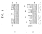
- FIGS. 1A and 1B show the constructions of the duplexer fabricated by using the conventional FBAR.
- FIG. 1A shows the duplexer fabricated in a manner that a transmitter filter 30 and a receiver filter 40 are prepared respectively, and bonded onto a printed circuit board (PCB) 10 with an isolation part 20 for isolating the two filters 30, 40 from each other.
- PCB printed circuit board
- the PCB 10 is a circuit board fabricated in a manner that various parts are densely embedded onto a flat board which is made of a phenol resin or an epoxy resin, and a circuit connecting the parts is densely integrated onto and fixed to the surface of the flat board.
- the transmitter filter 30 and the receiver filter 40 are respectively connected to an external electrode through a wire bonding method.
- the transmitter filter 30 and the receiver filter 40 are packaged separately and coupled to each other.
- the isolation part 20, which is separately fabricated, is bonded onto the flat board in the same process to fabricate the duplexer.
- the wire bonding there is a problem that a performance of an element is deteriorated due to a loss in the wiring and an increase in parasitic components.
- the final size of the duplexer element is increased due to the packaging size of the respective filters 30, 40 and the size of the isolation part 20 bonded between the filters 30, 40.
- the duplexer is not suitable for use in the miniaturized appliance such as a cellular phone and its fabricating cost is increased.
- FIG. 1B shows a duplexer built on a substrate using a Bragg type FBAR, which has a structure wherein a lower electrode 63, a piezoelectric layer 62, and an upper electrode 61 are deposited in order on a reflector layer 64 formed by depositing, in layers; materials having a large difference in acoustic impedance, as a transmitter/receiver filter.
- the receiver filter includes a serial resonator 60 and a parallel resonator 90
- the transmitter filter includes a serial resonator 80 and a parallel resonator 90, all of which are integrated onto one substrate 50.
- the Bragg type duplexer is fabricated on one substrate to realize a one-chip fabrication and has a strong structure.
- the Bragg type duplexer has problems in that it is difficult to accurately adjust the width of the respective layers, and the film is easily cracked due to the stress caused by the forming of the thick reflector layer.
- the Bragg type duplexer has a considerably lower Q value in comparison to a duplexer using an air gap type FBAR.
- a duplexer comprising:
- the invention thus provides a duplexer fabricated using an embedded printed circuit board (PCB) having an isolation part therein.
- PCB printed circuit board
- At least one of the first filter and the second filter includes at least one film bulk acoustic resonator which is fabricated by depositing a lower electrode, a piezoelectric layer, and an upper electrode in order.
- the first and second filters are bonded by a bumping method using a conductive bump, which bonds the first and second filters onto the upper side of the embedded PCB with a predetermined air gap therebetween.
- the isolation part prevents interference by making a phase difference of 90° between the frequencies of the signals inputted to the first and second filters.
- the isolation part includes a capacitor and a coil.
- the capacitor and the coil are fabricated by depositing a first metal layer, a dielectric, and a second metal layer on both sides of the PCB in order.
- the isolation part includes a transmission line fabricated between the plural PCBs deposited in order and having a length corresponding to 1/4 of the frequency of the signal passed by the first filter or the second filter.
- the isolation part uses a LC part including a capacitor and a coil.
- the capacitor and the coil are fabricated by depositing a first metal layer, a dielectric, and a second metal layer on both sides of the PCB in order.
- the step of fabricating the embedded PCB having the isolation part therein includes the steps of depositing the first metal layer on both sides of the PCB, depositing a photo resist layer on the first metal layer and forming a lower pattern of the coil by etching, depositing a first prepreg and the dielectric in order on the lower pattern of the coil, and patterning the dielectric in a predetermined pattern, depositing a second prepreg and a second metal layer on the patterned dielectric in order, fabricating an upper pattern of the coil by half-etching and patterning the second metal layer, exposing the lower pattern of the coil by drilling an area where the second metal layer is removed by the patterning, connecting the lower and upper patterns of the coil by metal-plating the drilled area, fabricating the coil by partially etching the metal-plated area, and depositing a third prepreg and a third metal layer on the coil in order.
- the isolation part includes a transmission line fabricated between the plural PCBs deposited in order and having a length corresponding to 1/4 of the frequency of the signal passed by the first filter or the second filter.
- the step (b) includes the steps of forming two through-holes by penetrating certain areas of the embedded PCB, plating upper and lower surfaces of the embedded PCB and both sidewalls of the through-hole with a fourth metal layer, providing a solder resist on an inside of the plated through-hole and the upper and lower surfaces of the embedded PCB, and plating the upper and lower surfaces of the embedded PCB with a fifth metal layer at an area where the solder resist is not deposited.
- the step (d) includes the steps of fabricating a conductive bump respectively on an upper portion of the plural pads, and bonding the first and second filters respectively to the conductive bump at a predetermined air gap with respect to the upper side of the embedded PCB.
- the step (e) may include the steps of fabricating a packaging substrate by etching a certain area of an additional PCB, coating a bonding material on an area except the etched area on the PCB, and bonding the packaging substrate to the embedded PCB so that the first and second filters are located in the etched area and spread away each other at a predetermined distance.
- the high-integrated duplexer having the isolation part in the PCB is fabricated.
- FIG. 2 is a view showing the structure of a duplexer finally fabricated according to an exemplary embodiment of the present invention.
- a transmitter filter 120 and a receiver filter 130 are bonded using ball bumps 150a, 150b.
- a packaging substrate 140 is bonded to the embedded PCB 200 with a predetermined distance from an upper portion of the transmitter filter (hereinafter, "first filter”) 120 and the receiver filter (hereinafter, "second filter”) 130.
- the embedded PCB 200 is a PCB having passive elements such as an inductor, a capacitor and a resistor therein.
- the PCB is fabricated in a manner that a layer such as a copper diaphragm is attached on a side of a phenolic resin insulating board or an epoxy resin insulating board and a required circuit is patterned by etching (removing except for the circuit on the board) along a wiring pattern of the circuit.
- the embedded PCB 200 is fabricated by depositing the several PCBs and building an inductor and a capacitor therein. In one embodiment, the embedded PCB 200 is fabricated in a structure having the built-in isolation part 110 between the PCBs.
- the first filter 120 and the second filter 130 are band pass filters which pass frequencies to be transmitted/received and cut off other frequencies.
- the first and second filters 120, 130 may be fabricated using more than one film bulk acoustic resonator (hereinafter, "FBAR").
- FBAR film bulk acoustic resonator
- the FBAR is fabricated in a structure that a lower electrode, a piezoelectric layer, and an upper electrode are deposited in that order. If a voltage is applied to the upper and lower electrodes, an electric field is generated between the two electrodes, and the piezoelectric layer produces a piezoelectric phenomenon that converts the electric field into a mechanical energy in the form of an acoustic wave to generate resonance. Accordingly, the FBAR can serve as a band pass filter to selectively pass signals of a frequency band in which resonance is generated. Meanwhile, the first and second filters 120, 130 may be implemented as a single filter by connecting several FBARs.
- the first and second filters 120, 130 are electrically connected to the embedded PCB 200 using the bumping method.
- the bumping method is performed by forming conductive balls 150a and 150b, which are external terminals in the form of protrusions having a size ranging from tens of ⁇ m to hundreds of ⁇ m, on the pads 160a, 160b with a metal material such as gold or solder and connecting the pads 160a, 160b with the two filters 120, 130 by the bumps 150a, 150b.
- the electrodes of the first and second filters 120, 130 are respectively connected to the conductive pads 160a, 160b on the embedded PCB 200 through the conductive bumps 150a, 150b alone.
- the length of the electrical wiring is shortened and an electrical resistance and noise are lessened to thereby enhance the electrical performance.
- the bumping method can be divided into an electroplating method which extracts metal by using a rectifier, and an electroless plating method which extracts metal by using a reducing agent.
- the bumping method may be classed into a gold (Au) bumping method, a solder bumping method, and a Ni/Cu bumping method.
- the gold (Au) bumping method is classified into a gold (Au) electroplating bumping method and an Au Stud bumping method.
- the solder bumping method is classed into a vapor deposition method, an electroplating method, a printing method, and a robotic ball placement method.
- the electroplating method of the solder bumping method may be used, which is suitable for the mass production and the accurate bumping fabrication.
- an air gap may be defined among the embedded PCB 200 and the first filter 120 and the second filter 130.
- the air gap prevents an acoustic wave generated in the first and second filters 120, 130 from being absorbed by the embedded PCB 200, to thereby obtain a high quality factor Q.
- the isolation part 110 in the embedded PCB 200 prevents inter-signal interference from being generated between the signals processed by the first filter 120 and the second filter 130.
- the isolation part 110 is included.
- the isolation part 110 may be implemented by fabricating a LC part in which a capacitor and a coil are deposited in order, or by a quarter-wave ( ⁇ /4) transmission line.
- the phase difference of 90° is obtained with respect to an input by the LC parallel circuit which is formed by depositing the capacitor and the coil in order.
- the phase difference of 90° is obtained by implementing the transmission line having a quarter length of the wave ⁇ of the transmitter signal and delaying the signal from the transmitter.
- a conventional duplexer has the structure with the isolation part 110 separately fabricated and bonded onto the PCB 200. According to the present embodiment, the isolation part 110 is built in the PCB 200 to reduce the entire size of the duplexer.
- the packaging substrate 140 is bonded at the upper portion of the embedded PCB 200 on which the first and second filters 120, 130 are bonded, at a predetermined distance from the first filter 120 and the second filter 130.
- the duplexer of FIG. 2 is fabricated by bonding the packaging substrate 140 so that the packaging substrate 140 seals and packages the PCB 200 to protect the PCB 200 from an external impact and to have the physical function and size, because the micro circuits such as the conductive bumps 150a, 150b, the first filter 120, and the second filter 130 are fragile.
- a process of fabricating the duplexer of FIG. 2 is discussed below.
- the embedded PCB 200 is fabricated having the isolation part 110 therein.
- the pads 160a, 160b are fabricated, and
- the first filter 120 and the second filter 130 are separately fabricated, which include more than one FBAR on which the lower electrode, the piezoelectric layer, and the upper electrode are deposited in order.
- the fabricated first and second filters 120, 130 are respectively bonded to the pads 160a, 160b formed on the embedded PCB 200, and (e) entire surface of the embedded PCB 200 is packaged.
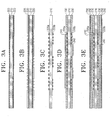
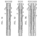
- FIGS. 3A to 3P illustrate one exemplary embodiment of the present invention, in which the embedded PCB 200 is fabricated using the LC part as the isolation part 110 (FIGS. 3A to 3K), and the pads 160a, 160b are fabricated (FIGS. 3I to 3P).
- FIGS. 4A and 4B show the process of fabricating the packaging substrate 140
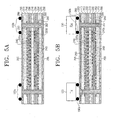
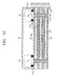
- FIGS. 5A to 5C show the process of bonding the embedded PCB 200, the first filter 120 and the second filter 130, and the packaging substrate 140.
- FIG. 3A shows the structure that a first metal layer 220 is deposited on both sides of a PCB 210.
- copper is used for the first metal layer 220.
- a photo resist layer 225 is deposited on a surface of the first metal layer 220 in a predetermined pattern as shown in FIG. 3B, and.exposed and developed.
- the first metal layer 220 is etched in a predetermined pattern, and lower patterns 220a, 220b of a coil are fabricated as shown in FIG. 3C.
- the micro circuit pattern formed on a photo resist-mask is transcribed to the coated photo resist layer 225 by irradiating light within an ultraviolet ray area of the light through the photo resist mask.
- the development is a process of resolving a PR area which has a weakened connection due to the exposure, by using a solvent.
- FIG. 3D shows the process of depositing a first prepreg 230 and a dielectric 240 on the lower patterns 220a, 220b of the coil in order, and patterning them.
- the first prepreg 230 is a material having a proper adhesive property used for fabricating a multi-layer printed wiring board.
- the first prepreg 230 is softened by impregnating a thermosetting resin on a material such a glass fabric.
- the dielectric 240 is deposited to form the capacitor and may use a general insulating material.
- a second prepreg 250 and a second metal layer 260 are deposited on the dielectric 240 in order (FIG. 3E), and the second metal layer 260 is half-etched (FIG. 3F). The half-etching process is performed to maintain an appropriate thickness of the second metal layer 260.
- the half-etched second metal layer 260 is etched in a predetermined pattern to form an upper pattern 260 of the coil (FIG. 3G), and drilled to expose the lower patterns 220a, 220b of the coil (FIG. 3H).
- a drilling process forms a hole (via hole) so that the upper/lower circuits of the board are electrically connected.
- a simple mechanical drilling method, a laser drilling method or a plasma drilling method may be used.
- a laser drilling method using a CO2 laser is widely practiced.
- the laser drilling method may use Nd-YAG laser for the micro fabrication.
- portion 267, exposed by the drilling, is metal-plated to connect the lower patterns 220a, 220b and the upper pattern 260 of the coil (FIG. 3I), and the upper pattern 260 is patterned to complete the coil (FIG. 3J).
- a third prepreg and a third metal layer are deposited in order (FIG. 3K).
- the embedded PCB 200 has the LC part built therein.
- FIGS. 3L to 3P show the process of fabricating the pads 160a, 160b on the embedded PCB 200.
- Plural through-holes 285 are formed penetrating through the embedded PCB 200 (FIG. 3L). As shown in FIG. 3L, two through-holes 285 are formed, but the number of the through-holes 285 may be adequately adjusted for use.
- the aforementioned drilling methods can be used.
- a fourth metal layer 287 is plated on both sidewalls of the through-hole 285 and the entire surface of the embedded PCB 200 (FIG. 3M), and patterned (FIG. 3N).
- solder resist 290 is deposited on an inside of the through-hole 285 and the entire surface of the embedded PCB 200, that are plated with the fourth metal layer 287, and patterned in a predetermined pattern (FIG. 3O).
- the solder resist 290 is a thermal-resistant cladding material to cover certain areas of the PCB 200. Since solders cannot adhere to the certain areas of the PCB 200 covered by the solder resist 290, the certain areas of the PCB 200 are protected from solding.
- the metal layers 220 to 295 may be copper.
- the process of fabricating the first and second filter 120, 130 may be performed according to a well-known FBAR fabrication process.
- the FBAR fabrication process is performed in a manner that an insulating layer is deposited on a separate silicon substrate, and a lower electrode, a piezoelectric layer and an upper electrode are deposited in order on the silicon substrate.
- An air gap type FBAR may be used, which is fabricated in a manner that a sacrificial layer is deposited on an insulating layer, and a lower electrode, a piezoelectric layer and an upper electrode are deposited, and the sacrificial layer is etched through a via hole.
- FIG. 4 shows the process of fabricating the packaging substrate 140 to protect the duplexer.
- a specific area of a separate PCB 140 is etched by using the photo resist layer (FIG. 4A), and a bonding material 141 is coated on a non-etched area for bonding.
- An adhesive such as an epoxy may be used as the bonding material.
- FIG. 5 shows the final process of fabricating the duplexer according to an embodiment of the present invention, in which separately-made first and second filters 120, 130 are bonded on the embedded PCB 200 of FIG. 3 and the packaging substrate 140 of FIG. 4 is bonded thereon.
- FIG. 5A shows the process of fabricating the conductive bumps 150a, 150b on the pad 295 which is exposed on the embedded PCB 200.
- the first and second filters 120, 130 are respectively connected to each conductive bumps 150a, 150b.
- Lower and upper electrodes of the first filter 120 are respectively connected to the conductive bump 150a
- the lower and upper electrodes of the second filter 130 are respectively connected to the conductive bump 150b.
- the packaging substrate 140 is bonded to the embedded PCB 200 using the bonding material 141, and the entire duplexer is packaged (FIG. 5C) to complete the process of fabricating the duplexer according to an embodiment of the present invention.
- the isolation part 110 may be implemented with a quarter-wave ( ⁇ /4) transmission line instead of the LC part.
- the embedded PCB 200 having the quarter-wave ( ⁇ /4) transmission line therein is fabricated in a manner that a metal layer is plated on a PCB and patterned, and then a PCB is additionally bonded thereon.
- the process of fabricating the embedded PCB 200 having the quarter-wave ( ⁇ /4) transmission line therein is generally well known, and therefore a detailed illustration thereof will be omitted for conciseness.
- the duplexer can have a reduced size. Hence, the high-integrated duplexer is achieved.
- the duplexer can have the reduced size and the integration and the isolation effect. Further, since the transmitter/receiver filters do not require additional packaging, the cost is reduced and the processes are simplified. Also, the parasitic components are decreased, because the filters are connected using the bump.
Landscapes
- Physics & Mathematics (AREA)
- Acoustics & Sound (AREA)
- Engineering & Computer Science (AREA)
- Microelectronics & Electronic Packaging (AREA)
- Electromagnetism (AREA)
- Piezo-Electric Or Mechanical Vibrators, Or Delay Or Filter Circuits (AREA)
- Control Of Motors That Do Not Use Commutators (AREA)
- Waveguide Switches, Polarizers, And Phase Shifters (AREA)
- Production Of Multi-Layered Print Wiring Board (AREA)
Applications Claiming Priority (2)
| Application Number | Priority Date | Filing Date | Title |
|---|---|---|---|
| KR1020030058072A KR100546832B1 (ko) | 2003-08-21 | 2003-08-21 | 임베디드 pcb 기판을 사용한 듀플렉서 및 그 제조 방법 |
| KR2003058072 | 2003-08-21 |
Publications (2)
| Publication Number | Publication Date |
|---|---|
| EP1508936A1 true EP1508936A1 (fr) | 2005-02-23 |
| EP1508936B1 EP1508936B1 (fr) | 2009-04-22 |
Family
ID=34056941
Family Applications (1)
| Application Number | Title | Priority Date | Filing Date |
|---|---|---|---|
| EP04253883A Expired - Lifetime EP1508936B1 (fr) | 2003-08-21 | 2004-06-29 | Méthode de fabrication d'un diplexeur avec circuit imprimé encastré et duplexeur fabriqué par cette méthode |
Country Status (5)
| Country | Link |
|---|---|
| US (2) | US7893792B2 (fr) |
| EP (1) | EP1508936B1 (fr) |
| JP (1) | JP2005073265A (fr) |
| KR (1) | KR100546832B1 (fr) |
| DE (1) | DE602004020716D1 (fr) |
Cited By (3)
| Publication number | Priority date | Publication date | Assignee | Title |
|---|---|---|---|---|
| GB2424328A (en) * | 2005-03-14 | 2006-09-20 | Agilent Technologies Inc | Monolithic device with acoustically isolated or decoupled FBAR-type resonator |
| US10489044B2 (en) | 2005-07-13 | 2019-11-26 | Microsoft Technology Licensing, Llc | Rich drag drop user interface |
| CN111261359A (zh) * | 2020-03-24 | 2020-06-09 | 福州瑞芯微电子股份有限公司 | 一种信号隔离器 |
Families Citing this family (17)
| Publication number | Priority date | Publication date | Assignee | Title |
|---|---|---|---|---|
| US7627552B2 (en) | 2003-03-27 | 2009-12-01 | Microsoft Corporation | System and method for filtering and organizing items based on common elements |
| US7552175B2 (en) * | 2004-04-30 | 2009-06-23 | Microsoft Corporation | Mechanism for controlling communication paths between conference members |
| KR100666693B1 (ko) | 2004-11-23 | 2007-01-11 | 삼성전자주식회사 | 모놀리식 듀플렉서 |
| KR100631212B1 (ko) | 2005-08-01 | 2006-10-04 | 삼성전자주식회사 | 모놀리식 듀플렉서 및 그 제조방법 |
| WO2007018227A1 (fr) * | 2005-08-11 | 2007-02-15 | Murata Manufacturing Co., Ltd. | Dispositif d'alimentation électrique à commutation de type isolant |
| US7483274B2 (en) * | 2005-09-29 | 2009-01-27 | Welch Allyn, Inc. | Galvanic isolation of a signal using capacitive coupling embedded within a circuit board |
| KR100916501B1 (ko) * | 2007-09-06 | 2009-09-08 | 엘지이노텍 주식회사 | 신호 처리 장치 |
| EP2309829A1 (fr) * | 2009-09-24 | 2011-04-13 | Harman Becker Automotive Systems GmbH | Carte à circuit multicouche |
| FR2961345A1 (fr) * | 2010-06-10 | 2011-12-16 | St Microelectronics Tours Sas | Circuit integre passif |
| WO2012155340A1 (fr) | 2011-05-17 | 2012-11-22 | Huawei Technologies Co., Ltd. | Module à hyperfréquences |
| KR101365368B1 (ko) | 2012-12-26 | 2014-02-24 | 삼성전기주식회사 | 공통모드필터 및 이의 제조방법 |
| CN104347526B (zh) * | 2013-07-29 | 2018-06-19 | 讯芯电子科技(中山)有限公司 | 双工器封装结构及制造方法 |
| US10291283B2 (en) * | 2016-04-01 | 2019-05-14 | Intel Corporation | Tunable radio frequency systems using piezoelectric package-integrated switching devices |
| US11563418B2 (en) | 2019-03-25 | 2023-01-24 | Skyworks Solutions, Inc. | Methods of manufacturing acoustic wave resonators with isolation |
| US12334618B2 (en) | 2020-01-24 | 2025-06-17 | Qm Technologies Aps | Rolled or folded filter comprising a flexible printed circuit board having first elongate signal tracks covered by an electromagnetically absorbing material |
| WO2021148621A1 (fr) | 2020-01-24 | 2021-07-29 | Qdevil Aps | Filtre à canaux multiples pour basses températures électroniques |
| KR20230020829A (ko) | 2021-08-04 | 2023-02-13 | 삼성전자주식회사 | 도전 패드를 포함하는 인쇄회로기판 및 이를 이용한 전자 장치 |
Citations (5)
| Publication number | Priority date | Publication date | Assignee | Title |
|---|---|---|---|---|
| US5703544A (en) * | 1996-03-13 | 1997-12-30 | Ericsson Inc. | RF printed circuit module and method of making same |
| EP1253713A2 (fr) * | 2001-04-23 | 2002-10-30 | Agilent Technologies, Inc. (a Delaware corporation) | Réglage des coefficients de couplage effectifs pour résonateurs acoustiques à ondes de volume |
| JP2002344349A (ja) * | 2001-05-11 | 2002-11-29 | Ube Electronics Ltd | 薄膜圧電共振器を用いた送受切換器 |
| US20030090338A1 (en) * | 2001-10-19 | 2003-05-15 | Kiyoshige Muramatsu | Branching filter and communication apparatus |
| US20040130410A1 (en) * | 2001-05-11 | 2004-07-08 | Kosuke Nishimura | Filter using film bulk acoustic resonator and transmission/reception switch |
Family Cites Families (19)
| Publication number | Priority date | Publication date | Assignee | Title |
|---|---|---|---|---|
| JP3156348B2 (ja) * | 1992-03-19 | 2001-04-16 | 富士通株式会社 | 弾性表面波フィルタとその製造方法 |
| JPH08181443A (ja) * | 1994-12-21 | 1996-07-12 | Murata Mfg Co Ltd | セラミック多層基板およびその製造方法 |
| KR0157284B1 (ko) | 1995-05-31 | 1999-02-18 | 김광호 | 솔더 볼 장착홈을 갖는 인쇄 회로 기판과 이를 사용한 볼 그리드 어레이 패키지 |
| US5910756A (en) * | 1997-05-21 | 1999-06-08 | Nokia Mobile Phones Limited | Filters and duplexers utilizing thin film stacked crystal filter structures and thin film bulk acoustic wave resonators |
| JP3575783B2 (ja) | 1997-05-21 | 2004-10-13 | 日本アビオニクス株式会社 | プリント配線板およびその製造方法 |
| JP3982876B2 (ja) * | 1997-06-30 | 2007-09-26 | 沖電気工業株式会社 | 弾性表面波装置 |
| US6239536B1 (en) * | 1998-09-08 | 2001-05-29 | Tfr Technologies, Inc. | Encapsulated thin-film resonator and fabrication method |
| US6262637B1 (en) | 1999-06-02 | 2001-07-17 | Agilent Technologies, Inc. | Duplexer incorporating thin-film bulk acoustic resonators (FBARs) |
| US6356455B1 (en) * | 1999-09-23 | 2002-03-12 | Morton International, Inc. | Thin integral resistor/capacitor/inductor package, method of manufacture |
| JP4529262B2 (ja) | 2000-09-14 | 2010-08-25 | ソニー株式会社 | 高周波モジュール装置及びその製造方法 |
| JP2002092427A (ja) | 2000-09-18 | 2002-03-29 | Nippon Paint Co Ltd | 商品受注・納入システム |
| JP2002185149A (ja) | 2000-12-15 | 2002-06-28 | Nippon Avionics Co Ltd | プリント配線板の製造方法 |
| US6424238B1 (en) * | 2001-01-08 | 2002-07-23 | Motorola, Inc. | Acoustic wave filter and method of forming the same |
| WO2002058233A1 (fr) | 2001-01-18 | 2002-07-25 | Infineon Technologies Ag | Dispositifs filtrants et procede de fabrication de ces derniers |
| JP3941416B2 (ja) * | 2001-04-26 | 2007-07-04 | ソニー株式会社 | 高周波モジュール装置及びその製造方法 |
| JP3937302B2 (ja) | 2001-12-10 | 2007-06-27 | 宇部興産株式会社 | 薄膜圧電共振器を用いたフィルタ及び送受切換器 |
| JP4079699B2 (ja) | 2001-09-28 | 2008-04-23 | 富士通株式会社 | 多層配線回路基板 |
| US6778038B2 (en) * | 2001-10-05 | 2004-08-17 | Tdk Corporation | Piezoelectric resonant filter, duplexer, and method of manufacturing same |
| DE20221966U1 (de) * | 2002-06-06 | 2010-02-25 | Epcos Ag | Mit akustischen Wellen arbeitendes Bauelement mit einem Anpaßnetzwerk |
-
2003
- 2003-08-21 KR KR1020030058072A patent/KR100546832B1/ko not_active Expired - Fee Related
-
2004
- 2004-06-29 EP EP04253883A patent/EP1508936B1/fr not_active Expired - Lifetime
- 2004-06-29 DE DE602004020716T patent/DE602004020716D1/de not_active Expired - Fee Related
- 2004-08-23 JP JP2004242915A patent/JP2005073265A/ja active Pending
- 2004-08-23 US US10/923,086 patent/US7893792B2/en not_active Expired - Fee Related
-
2011
- 2011-01-13 US US13/006,052 patent/US8418331B2/en not_active Expired - Fee Related
Patent Citations (5)
| Publication number | Priority date | Publication date | Assignee | Title |
|---|---|---|---|---|
| US5703544A (en) * | 1996-03-13 | 1997-12-30 | Ericsson Inc. | RF printed circuit module and method of making same |
| EP1253713A2 (fr) * | 2001-04-23 | 2002-10-30 | Agilent Technologies, Inc. (a Delaware corporation) | Réglage des coefficients de couplage effectifs pour résonateurs acoustiques à ondes de volume |
| JP2002344349A (ja) * | 2001-05-11 | 2002-11-29 | Ube Electronics Ltd | 薄膜圧電共振器を用いた送受切換器 |
| US20040130410A1 (en) * | 2001-05-11 | 2004-07-08 | Kosuke Nishimura | Filter using film bulk acoustic resonator and transmission/reception switch |
| US20030090338A1 (en) * | 2001-10-19 | 2003-05-15 | Kiyoshige Muramatsu | Branching filter and communication apparatus |
Non-Patent Citations (1)
| Title |
|---|
| PATENT ABSTRACTS OF JAPAN vol. 2003, no. 03 5 May 2003 (2003-05-05) * |
Cited By (5)
| Publication number | Priority date | Publication date | Assignee | Title |
|---|---|---|---|---|
| GB2424328A (en) * | 2005-03-14 | 2006-09-20 | Agilent Technologies Inc | Monolithic device with acoustically isolated or decoupled FBAR-type resonator |
| US7248131B2 (en) | 2005-03-14 | 2007-07-24 | Avago Technologies Wireless Ip (Singapore) Pte. Ltd. | Monolithic vertical integration of an acoustic resonator and electronic circuitry |
| GB2424328B (en) * | 2005-03-14 | 2009-08-19 | Agilent Technologies Inc | Acoustic resonator |
| US10489044B2 (en) | 2005-07-13 | 2019-11-26 | Microsoft Technology Licensing, Llc | Rich drag drop user interface |
| CN111261359A (zh) * | 2020-03-24 | 2020-06-09 | 福州瑞芯微电子股份有限公司 | 一种信号隔离器 |
Also Published As
| Publication number | Publication date |
|---|---|
| DE602004020716D1 (de) | 2009-06-04 |
| US20110107570A1 (en) | 2011-05-12 |
| JP2005073265A (ja) | 2005-03-17 |
| US7893792B2 (en) | 2011-02-22 |
| US20050105478A1 (en) | 2005-05-19 |
| EP1508936B1 (fr) | 2009-04-22 |
| KR20050020289A (ko) | 2005-03-04 |
| US8418331B2 (en) | 2013-04-16 |
| KR100546832B1 (ko) | 2006-01-26 |
Similar Documents
| Publication | Publication Date | Title |
|---|---|---|
| US8418331B2 (en) | Method of fabricating a duplexer using an embedded PCB | |
| US10305444B2 (en) | Electronic component module | |
| KR100910425B1 (ko) | 탄성파 디바이스 | |
| US7940146B2 (en) | Boundary acoustic wave element, boundary acoustic wave device, and manufacturing methods for the same | |
| CN1638272B (zh) | 表面弹性波装置、电子电路装置、通信装置及电子装置 | |
| KR100949224B1 (ko) | 필터 회로 장치 및 그 제조 방법 | |
| US9197192B2 (en) | Electronic component including a surface acoustic wave element and a pillar member | |
| US20110193650A1 (en) | Duplexer, Communication Module Component, and Communication Device | |
| US11139266B2 (en) | Manufacturing method for electronic component, and electronic component | |
| JP4926179B2 (ja) | 分波器デバイス用回路基板、分波器、及び通信装置 | |
| KR20040002389A (ko) | 고주파 모듈 및 그 제조 방법 | |
| KR101319195B1 (ko) | 분파기 | |
| US11069645B2 (en) | Electronic component module | |
| KR20170020835A (ko) | 체적 음향 공진기 구조 및 제조 방법 | |
| KR100498041B1 (ko) | 기판 접합을 이용하여 제조된 단일칩 듀플렉서 및 그 제조방법 | |
| US11257730B2 (en) | Electronic component module, and manufacturing method for electronic component module | |
| KR100400062B1 (ko) | 무선 헬리컬 안테나 제조방법 | |
| KR100560417B1 (ko) | 단일칩 듀플레서 및 그 제조방법 |
Legal Events
| Date | Code | Title | Description |
|---|---|---|---|
| PUAI | Public reference made under article 153(3) epc to a published international application that has entered the european phase |
Free format text: ORIGINAL CODE: 0009012 |
|
| AK | Designated contracting states |
Kind code of ref document: A1 Designated state(s): AT BE BG CH CY CZ DE DK EE ES FI FR GB GR HU IE IT LI LU MC NL PL PT RO SE SI SK TR |
|
| AX | Request for extension of the european patent |
Extension state: AL HR LT LV MK |
|
| 17P | Request for examination filed |
Effective date: 20050413 |
|
| AKX | Designation fees paid |
Designated state(s): DE ES FR GB NL SE |
|
| 17Q | First examination report despatched |
Effective date: 20060119 |
|
| 17Q | First examination report despatched |
Effective date: 20060119 |
|
| GRAP | Despatch of communication of intention to grant a patent |
Free format text: ORIGINAL CODE: EPIDOSNIGR1 |
|
| GRAS | Grant fee paid |
Free format text: ORIGINAL CODE: EPIDOSNIGR3 |
|
| GRAA | (expected) grant |
Free format text: ORIGINAL CODE: 0009210 |
|
| AK | Designated contracting states |
Kind code of ref document: B1 Designated state(s): DE ES FR GB NL SE |
|
| REG | Reference to a national code |
Ref country code: GB Ref legal event code: FG4D |
|
| REF | Corresponds to: |
Ref document number: 602004020716 Country of ref document: DE Date of ref document: 20090604 Kind code of ref document: P |
|
| PG25 | Lapsed in a contracting state [announced via postgrant information from national office to epo] |
Ref country code: ES Free format text: LAPSE BECAUSE OF FAILURE TO SUBMIT A TRANSLATION OF THE DESCRIPTION OR TO PAY THE FEE WITHIN THE PRESCRIBED TIME-LIMIT Effective date: 20090802 |
|
| PG25 | Lapsed in a contracting state [announced via postgrant information from national office to epo] |
Ref country code: SE Free format text: LAPSE BECAUSE OF FAILURE TO SUBMIT A TRANSLATION OF THE DESCRIPTION OR TO PAY THE FEE WITHIN THE PRESCRIBED TIME-LIMIT Effective date: 20090722 |
|
| PLBE | No opposition filed within time limit |
Free format text: ORIGINAL CODE: 0009261 |
|
| STAA | Information on the status of an ep patent application or granted ep patent |
Free format text: STATUS: NO OPPOSITION FILED WITHIN TIME LIMIT |
|
| REG | Reference to a national code |
Ref country code: FR Ref legal event code: ST Effective date: 20100226 |
|
| 26N | No opposition filed |
Effective date: 20100125 |
|
| PG25 | Lapsed in a contracting state [announced via postgrant information from national office to epo] |
Ref country code: FR Free format text: LAPSE BECAUSE OF NON-PAYMENT OF DUE FEES Effective date: 20090630 |
|
| PG25 | Lapsed in a contracting state [announced via postgrant information from national office to epo] |
Ref country code: DE Free format text: LAPSE BECAUSE OF NON-PAYMENT OF DUE FEES Effective date: 20100101 |
|
| REG | Reference to a national code |
Ref country code: NL Ref legal event code: V1 Effective date: 20150101 |
|
| PG25 | Lapsed in a contracting state [announced via postgrant information from national office to epo] |
Ref country code: NL Free format text: LAPSE BECAUSE OF NON-PAYMENT OF DUE FEES Effective date: 20150101 |
|
| REG | Reference to a national code |
Ref country code: NL Ref legal event code: BK Free format text: TEN ONTERECHTE VERVALLEN OP 2015.01.01 PUBLIKATIE I.E. 2015/04 UITGEGEVEN 2015.01.21 |
|
| PG25 | Lapsed in a contracting state [announced via postgrant information from national office to epo] |
Ref country code: NL Free format text: LAPSE BECAUSE OF NON-PAYMENT OF DUE FEES Effective date: 20150101 |
|
| PGRI | Patent reinstated in contracting state [announced from national office to epo] |
Ref country code: NL Effective date: 20150121 |
|
| PGFP | Annual fee paid to national office [announced via postgrant information from national office to epo] |
Ref country code: NL Payment date: 20200521 Year of fee payment: 17 |
|
| PGFP | Annual fee paid to national office [announced via postgrant information from national office to epo] |
Ref country code: GB Payment date: 20200522 Year of fee payment: 17 |
|
| REG | Reference to a national code |
Ref country code: NL Ref legal event code: MM Effective date: 20210701 |
|
| GBPC | Gb: european patent ceased through non-payment of renewal fee |
Effective date: 20210629 |
|
| PG25 | Lapsed in a contracting state [announced via postgrant information from national office to epo] |
Ref country code: GB Free format text: LAPSE BECAUSE OF NON-PAYMENT OF DUE FEES Effective date: 20210629 |
|
| PG25 | Lapsed in a contracting state [announced via postgrant information from national office to epo] |
Ref country code: NL Free format text: LAPSE BECAUSE OF NON-PAYMENT OF DUE FEES Effective date: 20210701 |