EP1509038B1 - Capteur d'image rapide - Google Patents
Capteur d'image rapide Download PDFInfo
- Publication number
- EP1509038B1 EP1509038B1 EP04250088A EP04250088A EP1509038B1 EP 1509038 B1 EP1509038 B1 EP 1509038B1 EP 04250088 A EP04250088 A EP 04250088A EP 04250088 A EP04250088 A EP 04250088A EP 1509038 B1 EP1509038 B1 EP 1509038B1
- Authority
- EP
- European Patent Office
- Prior art keywords
- voltage
- mos transistor
- reset
- sensing device
- image sensing
- Prior art date
- Legal status (The legal status is an assumption and is not a legal conclusion. Google has not performed a legal analysis and makes no representation as to the accuracy of the status listed.)
- Expired - Lifetime
Links
Images





Classifications
-
- H—ELECTRICITY
- H04—ELECTRIC COMMUNICATION TECHNIQUE
- H04N—PICTORIAL COMMUNICATION, e.g. TELEVISION
- H04N25/00—Circuitry of solid-state image sensors [SSIS]; Control thereof
- H04N25/70—SSIS architectures; Circuits associated therewith
- H04N25/76—Addressed sensors, e.g. MOS or CMOS sensors
- H04N25/77—Pixel circuitry, e.g. memories, A/D converters, pixel amplifiers, shared circuits or shared components
-
- H—ELECTRICITY
- H04—ELECTRIC COMMUNICATION TECHNIQUE
- H04N—PICTORIAL COMMUNICATION, e.g. TELEVISION
- H04N25/00—Circuitry of solid-state image sensors [SSIS]; Control thereof
- H04N25/60—Noise processing, e.g. detecting, correcting, reducing or removing noise
- H04N25/65—Noise processing, e.g. detecting, correcting, reducing or removing noise applied to reset noise, e.g. KTC noise related to CMOS structures by techniques other than CDS
-
- H—ELECTRICITY
- H04—ELECTRIC COMMUNICATION TECHNIQUE
- H04N—PICTORIAL COMMUNICATION, e.g. TELEVISION
- H04N25/00—Circuitry of solid-state image sensors [SSIS]; Control thereof
- H04N25/70—SSIS architectures; Circuits associated therewith
- H04N25/76—Addressed sensors, e.g. MOS or CMOS sensors
- H04N25/77—Pixel circuitry, e.g. memories, A/D converters, pixel amplifiers, shared circuits or shared components
- H04N25/771—Pixel circuitry, e.g. memories, A/D converters, pixel amplifiers, shared circuits or shared components comprising storage means other than floating diffusion
Definitions
- the present invention relates to a pixel circuit of a high-speed CMOS image sensor.
- a CCD image sensor In a general pixel circuit of a CMOS image sensor, signal charges are stored and read, then signal charges are initialized (reset) for each horizontal line. Since the start timing of reset and the start of signal charging differ depending on the horizontal line, distortion occurs in an image which has a large movement.
- a CCD image sensor can reset all the pixels at the same time and start signal storing at the same time. This is called an “electronic shutter operation” or "global shutter”.
- Document US-A-5,488,415 discloses a photoelectric conversion detection cell including a photodiode, a storage capacitor for storing a photo-induced charge induced in the photodiode, and a transfer transistor for transferring the photo-induced charge induced in the photodiode to the storage capacitor, the source of the transfer transistor being connected to the photodiode, the drain of the transfer transistor being connected to the storage capacitor, the photoelectric conversion detection cell further including an inverting amplifier, the input of the inverting amplifier being connected to the photodiode, the output of the inverting amplifier being connected to the gate of the transfer transistor.
- Document WO-A-99/44359 discloses a method for reducing reset noise of a sensor having a pixel and further controlling a reset command signal, a sample signal, and a read command signal with a controller (560).
- a high-speed image sensor has remarkable improvements in performance due to the recent advancements in CMOS image sensor technology, but also has some problems.
- the following is demanded particularly in the functions and performance of the pixel section.
- the present invention provides a pixel circuit of a high-speed CMOS image sensor which can satisfy these demands, as set out in claim 1.
- the present invention allows implementing the electronic shutter operation, a reset noise reduction, and a voltage amplification within a pixel using a simple circuit.
- Fig. 1 shows a concrete example of the circuit according to the present invention.
- the section indicated by 1 comprise a photo-diode PD as a photo-electric conversion element; a transfer gate transistor MT, and reset transistor MR.
- the charges generated by the irradiation of light in the cathode section of the photo-diode are stored, and the charges Q are transferred to the section indicated by V FD by operating the control line TX (hereafter referred to as "TX"). If the parasitic capacitance generated in the V FD section at this time is C FD , then a signal voltage change corresponding to Q/C FD is generated.
- the section indicated by 1 corresponds to the section indicated by 1 of the conventional 4-transistor pixel circuit shown in Fig. 2 .
- a pinned photo-diode may be used.
- the voltage of V FD is directly read out using the buffer circuit comprising n-channel transistors MIN and MX and the current source load transistor which is connected to the vertical signal line.
- the signal for which the electronic shutter operation, voltage amplification and reset noise reduction were performed in the section indicated by 2 in Fig. 1 is read out using the buffer circuit and the current source load transistor in the section indicated by 3 in Fig. 1 .
- a p-channel transistor is used since the output voltage in section 2 is at low voltage level.
- the control line SX is for controlling the output gate of the buffer circuit.
- Fig. 3 shows a diagram depicting the operation when circuits 1 and 2 are combined. To simplify explanation, a concrete value of voltage is used, but the voltage] to be used is not limited to the voltage used here.
- the control line R hereafter referred to as "R”
- the reset transistor MR is ON
- the voltage of V FD is at reset voltage V R (2.0V in this case).
- the control line SR (hereafter referred to as "SR") is changed from 3V to 0V
- the voltage of V 1 is set to V RS (about 2.0V).
- V RS about 2.0V
- the voltage of V 2 rises to the voltage of V RS .
- SR is returned to 3V and R is set to 0V.
- the voltage of V FD becomes a voltage slightly lower than the reset voltage V R due to feed through, and the voltage of V FD at this time becomes V FD0 .
- This V FD0 includes a reset noise component which is generated by thermal noise, and remains as electric charges. Then the voltage of V 2 is dropped to 0V by setting the control line SS (hereafter referred to as "SS") from 0V to 3V, and by this, the charges stored at section V 1 flow over the potential barrier created by the p-channel MOS transistor 4 and move to the V 2 side, and the voltage of V 1 gradually drops. Then SS is returned to 0V. At this stage, preparation for signal amplification, electronic shutter and reset noise reduction operation is complete.
- SS control line SS
- the charges stored by the photo-diode are transferred to the V FD side, and the voltage thereof drops.
- the amount of this voltage change is assumed to be ⁇ V FD .
- the potential barrier of the p-channel MOS transistor 4 becomes low, and charges flow from V 1 to V 2 , and the voltage of V 1 drops.
- the amount of this voltage change is ⁇ V 1 , which is ideally equal to ⁇ V FD , but is smaller than ⁇ V FD since the rate of change of the surface potential of the channel with respect to the gate voltage of the p-channel MOS transistor 4 is not 1.
- the signal voltage can be amplified by taking the ratio of C 1 and C 2 to be large. Also the change of V 2 is in proportion to the changed amount of V FD , so the reset noise generated at V FD can be removed.
- the reset noise which is the same amount of reset noise component sampled and included in the V FD0 before opening TX, is included in the voltage after TX is opened and a ⁇ V FD change occurs. So the reset noise is removed by taking out the changed amount ⁇ V FD and amplifying it.
- the p-channel MOS transistor 4 operates in the weak inversion region, and a flow out of charges is generated by the diffusion of carriers, so it takes a long time until the flow out becomes completely zero. If the next operation is begun in a status where the flow out is not zero, nonlinearity is generated. Therefore another possible method is to apply the pulse voltage, of which the initial voltage is about 0V to several tens mV, to V P , so as to accelerate the flow out of charges from V 1 .
- the MOS transistor 4 which is the MOS transistor for supplying charges from the power supply voltage VRS to the point V 1 , and the MOS transistor of the output buffer, are p-channel types, and the other MOS transistors are n-channel types.
- Most MOS transistors however are operating as transfer gates, and an n-channel type can be used instead of a p-channel type, or vice versa, which is obvious to experts in this field. This is also the same for the MOS transistors of the signal line.
- control signals must be considered when a different conductive type MOS transistor is used.
- C 1 is created by the gate capacitance of the n-channel MOS transistor
- C 2 is created by the gate capacitance of the p-channel MOS transistor, so the former gate voltage for operation is a high voltage, around 2 - 3V, and the latter gate voltage is a low voltage, about 0V to 1V. Therefore a transistor operates in a strong inversion status where the gate oxide film capacitance can be used, which is a capacitance that depends little on voltage.
- Fig. 4 shows the configuration of the entire image sensor where the circuit in Fig. 2 is used for the pixel section.
- Fig. 5 is the timing chart thereof..
- electronic shutter, amplification and noise cancellation operations are performed by each control signal R, TX and SS, and for the output signal thereof (V2 in Fig. 1 ), vertical reading and horizontal reading are performed for each row using the control signals (SS i , SX i ) which are output from the vertical shift register, and the result is output to the outside.
- the noise cancellation operation for removing fixed pattern noise which is generated due to the characteristic dispersion of the buffer amplifier at the section indicated by 3 in Fig.1 , is performed by the noise cancellation circuit.
- SX of the pixel in the horizontal line is set to 0V, and the voltage of V 2 is read by this.
- the voltage of V 2 is read, then SS of the horizontal line is set to 3V to set V 2 of the pixel section to 0V, since SS was also used for the electronic shutter operation.
- the noise cancellation circuit the difference of the voltage of V 2 which was read and the voltage when V 2 is set to 0V is determined so as to acquire the amount of change ⁇ V 2 of the voltage of V 2 , and the fixed pattern noise generated by the buffer amplifier can be removed.
- a generally used noise cancellation circuit for image sensors can be used, and description thereof is omitted here since there are no specific features unique to the present invention.
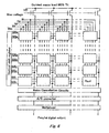
- Fig. 7 shows a configuration when a high-speed image sensor is implemented using the circuit in Fig. 1 .
- the above configuration can be applied when the photo-gate shown in Fig. 7 is used.
- the difference in this case is that high voltage (e.g. 3V) is applied to TX when charges are stored, and low voltage (e.g. 0V) is applied when charges are transferred.
- high voltage e.g. 3V
- low voltage e.g. 0V
- Fig. 8 shows another pixel circuit which has an electronic shutter operation and reset noise and fixed pattern noise removal functions.
- R is set to High to turn the reset transistor ON, and VFD is set to reset voltage VR.
- the voltage at this time is read via the source follower buffer, and is stored in the transistorfor capacitance 5 by setting SR to High.
- TX is opened and the voltage of VFD is changed (dropped) by transferring the signal charges to the VFD section.
- This voltage is read via the source follower buffer, and SS is set to High to store it in the transistor for capacitance 6.
- An electronic shutter operation is performed by executing this storage operation simultaneously for all the pixels. In the case of this circuit as well, a system using photo-gates instead of photo-diodes is possible.
- S in Fig. 8 is a control signal for decreasing power consumption by cutting the current that flows through the source follower circuit when reading is not performed, and the transistor to which S is connected is a switch for this operation.
- the signals stored for the two capacitors are read out to outside the image array via the respective buffer circuits. Selection for reading out is executed by setting RS to High. By this read out operation, fixed pattern noise due to the dispersion of the circuits and reset noise are cancelled.
- Fig. 9 shows an example of circuits for canceling noise lining up in columns.
- V out R and V out S in Fig. 8 are connected respectively to V in- and V in+ in Fig. 9 .
- RS in Fig. 8 In vertical reading from the image sensor, RS in Fig. 8 is set to High, and signals in one horizontal line are read out.
- ⁇ 1 in Fig. 9 is set to High first, and the switch to which this is connected is turned ON.
- the capacitor C2 is connected to the reference voltage V ref .
- ⁇ 1 is set to Low
- ⁇ 2 is set to High
- the capacitor C2 is connected to output.
- RR in Fig. 8 is set to High, then signals which are in proportion to the difference of the voltages stored in the capacitors 5 and 6 in Fig. 8 and which are amplified by ratio C1/C2 are generated in the output in Fig. 9 .
- the fixed pattern noise which the source follower of the output in Fig. 9 generates is cancelled, and the 1/f noise can be decreased.
- the circuit in Fig. 8 can be simplified, as shown in Fig. 10 .
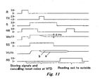
- Fig. 11 shows the operation timing.
- the voltage of the VFD section is initialized to the reset voltage (2V in this case) by setting R to High.
- S is set to High to operate the first source follower.
- the voltage difference of VFD appears in the output of the source follower.
- RR has been set to High in advance, and the transistor to which RR is connected has been turned ON, so by setting SS to High, the reset level is supplied to the transistors for capacitance 5 and 6, then by returning RR to Low, the reset level is stored (sampled and held) in the transistors for capacitance 6.
- the voltage of VFD is changed (dropped) by setting TX to High and transferring charges from the photo-diode to the VFD section.
- the voltage stored in the two capacitors are sequentially read out to the outside to an image array, but noise cancellation processing is actually performed at this time.
- the noise cancellation circuit which is disposed in an external column of the image array, the one shown in Fig. 9 can be used.
- Fig. 12 The general configuration of the image sensor, in this case, is as shown in Fig. 12 . Signals propagate through two lines from each pixel in the vertical direction.
- Fig. 12 shows the case when horizontal scanning is performed after vertical reading, and image signals are read out as time series signals via one output line, but in order to read images at high-speed, a configuration similar to Fig. 6 may be used, where a plurality of high-speed A/D converters are lined up to perform A/D conversion in parallel, and signals are output in parallel via a plurality of digital signal lines.
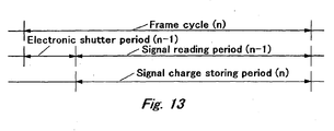
- the time breakdown of the electronic shutter operation, signal reading and signal charge storing in a one frame cycle is as shown in Fig. 13 , for example,
- the electronic shutter operation, signal voltage amplification and reset noise reduction processing are performed at the beginning of the n-th frame for the signal charges stored in the (n-1)-th frame, and the signals are read out from the pixel section by vertical and horizontal scanning using the remaining period of the n-th frame.
- signal charge storing in the n-th frame is performed during this period.
- the present invention allows implementing the electronic shutter operation, reset noise reduction and voltage amplification using simple circuits, which can be installed at the pixel section.
Landscapes
- Engineering & Computer Science (AREA)
- Multimedia (AREA)
- Signal Processing (AREA)
- Transforming Light Signals Into Electric Signals (AREA)
- Solid State Image Pick-Up Elements (AREA)
Claims (5)
- Capteur d'image rapide, comprenant dans un pixel :des moyens de conversion photoélectrique (PD) ;des moyens de grille (MT) comprenant un premier transistor MOS pour transférer des charges de signal générées par lesdits moyens de conversion photoélectrique à une étape suivante (2) ;des moyens de stockage pour stocker les charges de signal depuis lesdits moyens de grille ;des moyens de réinitialisation (MR) comprenant un deuxième transistor MOS pour réinitailiser les charges de signal desdits moyens de stockage ; etdes moyens de lecture (3) pour lire des signaux de tension depuis lesdits moyens de stockage ;dans lequel une sortie desdits moyens de conversion photoélectrique (PD) est connectée à une source du premier transistor MOS (MT) pour agir comme une grille de transfert, une source du deuxième transistor MOS (MR) à réinitialiser est connectée à un drain dudit premier transistor MOS (MT) ;dans lequel une tension de réinitialisation (VR) est appliquée à la source dudit deuxième transistor MOS (MR) ;caractérisé en ce que le capteur d'image rapide comprend en outre :des moyens, comprenant un troisième transistor MOS, pour réduire le bruit de réinitialisation (4) sur la base d'une tension de réinitialisation (VR) par lesdits moyens de réinitialisation (MR) et les signaux de tension stockés dans lesdits moyens de stockage ;dans lequel une grille du troisième transistor MOS (4) pour réinitialiser la réduction du bruit est connectée au drain dudit premier transistor MOS (MT), dans lequel un premier condensateur est connecté entre une première tension de référence (Vp) et un drain dudit troisième transistor MOS (4) et un second condensateur est connecté entre une seconde tension de référence (VDD) et une source dudit troisième transistor MOS, et dans lequel des premiers et seconds moyens de chargement/déchargement pour charger/décharger lesdits premier et second condensateurs sont connectés à la source et au drain dudit troisième transistor MOS (4) respectivement.
- Capteur d'image rapide selon la revendication 1, dans lequel la capacité dudit premier condensateur est réglée pour être plus élevée que celle dudit second condensateur, et la tension est amplifiée alors que les charges sont transférées lorsque les charges de signal stockées dans le premier condensateur sont transférées au second condensateur, par ledit troisième transistor MOS (4).
- Capteur d'image rapide selon la revendication 1, dans lequel la conductivité est fournie au canal dudit troisième transistor MOS (4) par des porteuses qui sont différentes de celles du canal dudit deuxième transistor MOS (MR).
- Capteur d'image rapide selon la revendication 1, comprenant en outre des moyens pour commander lesdits premiers et seconds moyens de chargement/déchargement, et la conductivité/non-conductivité desdits premier et deuxième transistors MOS (MT, MR).
- Capteur d'image rapide selon la revendication 1,
dans lequel les moyens de mémoire (3) comprennent :des premiers moyens de mémoire (5) pour stocker la tension à la réinitialisation des charges de signal ; etdes seconds moyens de mémoire (6) pour stocker la tension de signal provenant des moyens de conversion photoélectrique,et dans lequel une différence des tensions stockées dans les premiers et seconds moyens de mémoire est lue hors de la matrice d'image, et est sortie comme une tension différentielle pour annuler le bruit de réinitialisation.
Applications Claiming Priority (2)
| Application Number | Priority Date | Filing Date | Title |
|---|---|---|---|
| JP2003295027A JP4288346B2 (ja) | 2003-08-19 | 2003-08-19 | 撮像装置及び画素回路 |
| JP2003295027 | 2003-08-19 |
Publications (3)
| Publication Number | Publication Date |
|---|---|
| EP1509038A2 EP1509038A2 (fr) | 2005-02-23 |
| EP1509038A3 EP1509038A3 (fr) | 2008-01-23 |
| EP1509038B1 true EP1509038B1 (fr) | 2011-04-20 |
Family
ID=34056217
Family Applications (1)
| Application Number | Title | Priority Date | Filing Date |
|---|---|---|---|
| EP04250088A Expired - Lifetime EP1509038B1 (fr) | 2003-08-19 | 2004-01-09 | Capteur d'image rapide |
Country Status (4)
| Country | Link |
|---|---|
| US (1) | US6963116B2 (fr) |
| EP (1) | EP1509038B1 (fr) |
| JP (1) | JP4288346B2 (fr) |
| DE (1) | DE602004032294D1 (fr) |
Families Citing this family (26)
| Publication number | Priority date | Publication date | Assignee | Title |
|---|---|---|---|---|
| JP4455215B2 (ja) * | 2004-08-06 | 2010-04-21 | キヤノン株式会社 | 撮像装置 |
| US8072520B2 (en) * | 2004-08-30 | 2011-12-06 | Micron Technology, Inc. | Dual pinned diode pixel with shutter |
| JP4640102B2 (ja) * | 2005-10-20 | 2011-03-02 | 日本ビクター株式会社 | 全方位カメラ |
| JP4862129B2 (ja) * | 2005-12-02 | 2012-01-25 | 株式会社Jvcケンウッド | 車載カメラ装置を用いた運転支援装置 |
| JP4743007B2 (ja) | 2006-06-16 | 2011-08-10 | ソニー株式会社 | 画像処理装置および画像処理方法、記録媒体、並びに、プログラム |
| US7669720B2 (en) | 2006-12-15 | 2010-03-02 | General Electric Company | Functional polyarylethers |
| US7681741B2 (en) | 2006-12-15 | 2010-03-23 | General Electric Company | Functional polyarylethers |
| WO2010023903A1 (fr) * | 2008-09-01 | 2010-03-04 | 株式会社ニコン | Elément d'imagerie et dispositif d'imagerie |
| JP4957925B2 (ja) * | 2009-01-30 | 2012-06-20 | 株式会社ブルックマンテクノロジ | 増幅型固体撮像装置 |
| JP5369779B2 (ja) | 2009-03-12 | 2013-12-18 | ソニー株式会社 | 固体撮像装置、固体撮像装置の駆動方法および電子機器 |
| JP5257176B2 (ja) | 2009-03-18 | 2013-08-07 | ソニー株式会社 | 固体撮像装置、固体撮像装置の駆動方法および電子機器 |
| US20100271517A1 (en) * | 2009-04-24 | 2010-10-28 | Yannick De Wit | In-pixel correlated double sampling pixel |
| JP5272916B2 (ja) * | 2009-06-17 | 2013-08-28 | ペンタックスリコーイメージング株式会社 | 撮像装置 |
| JP5436173B2 (ja) | 2009-12-02 | 2014-03-05 | キヤノン株式会社 | 固体撮像装置 |
| US8907388B2 (en) * | 2010-02-05 | 2014-12-09 | National University Corporation Shizuoka University | Optical-information acquiring element, optical information acquiring element array, and hybrid solid-state imaging device |
| KR102509203B1 (ko) * | 2014-08-29 | 2023-03-14 | 가부시키가이샤 한도오따이 에네루기 켄큐쇼 | 촬상 장치 및 전자 기기 |
| JP6525694B2 (ja) * | 2015-04-08 | 2019-06-05 | キヤノン株式会社 | 撮像装置、撮像システム、および、撮像装置の駆動方法 |
| JP6492991B2 (ja) | 2015-06-08 | 2019-04-03 | 株式会社リコー | 固体撮像装置 |
| JP6832649B2 (ja) | 2016-08-17 | 2021-02-24 | ブリルニクス インク | 固体撮像装置、固体撮像装置の駆動方法、および電子機器 |
| US10855927B2 (en) | 2017-03-08 | 2020-12-01 | Samsung Electronics Co., Ltd. | Event detecting device including an event signal generator and an output signal generator |
| US10516841B2 (en) | 2017-03-08 | 2019-12-24 | Samsung Electronics Co., Ltd. | Pixel, pixel driving circuit, and vision sensor including the same |
| JP7330124B2 (ja) * | 2020-03-19 | 2023-08-21 | 株式会社東芝 | 固体撮像装置 |
| JP2023104261A (ja) | 2022-01-17 | 2023-07-28 | ブリルニクス シンガポール プライベート リミテッド | 固体撮像装置、固体撮像装置の駆動方法、および電子機器 |
| US20250374694A1 (en) * | 2022-01-26 | 2025-12-04 | Sony Semiconductor Solutions Corporation | Photodetection device |
| JP2024010357A (ja) | 2022-07-12 | 2024-01-24 | ブリルニクス シンガポール プライベート リミテッド | 固体撮像装置、固体撮像装置の駆動方法、および電子機器 |
| JP2024040751A (ja) | 2022-09-13 | 2024-03-26 | ブリルニクス シンガポール プライベート リミテッド | 固体撮像装置、固体撮像装置の駆動方法、および電子機器 |
Family Cites Families (6)
| Publication number | Priority date | Publication date | Assignee | Title |
|---|---|---|---|---|
| US5488415A (en) | 1993-07-09 | 1996-01-30 | Olympus Optical Co., Ltd. | Solid-state image pickup device having a photoelectric conversion detection cell with high sensitivity |
| EP0878007B1 (fr) | 1996-01-22 | 2005-05-11 | California Institute Of Technology | Reseau de detecteurs a pixels actifs obturables electroniquement |
| US5986297A (en) | 1996-05-22 | 1999-11-16 | Eastman Kodak Company | Color active pixel sensor with electronic shuttering, anti-blooming and low cross-talk |
| US6243134B1 (en) | 1998-02-27 | 2001-06-05 | Intel Corporation | Method to reduce reset noise in photodiode based CMOS image sensors |
| GB0015685D0 (en) * | 2000-06-28 | 2000-08-16 | Vlsi Vision Ltd | Image sensors with multiple integration read cycle |
| EP1301028A1 (fr) * | 2001-10-05 | 2003-04-09 | STMicroelectronics Limited | Améliorations concernant les capteurs d'images CMOS |
-
2003
- 2003-08-19 JP JP2003295027A patent/JP4288346B2/ja not_active Expired - Lifetime
- 2003-12-22 US US10/740,550 patent/US6963116B2/en not_active Expired - Fee Related
-
2004
- 2004-01-09 EP EP04250088A patent/EP1509038B1/fr not_active Expired - Lifetime
- 2004-01-09 DE DE602004032294T patent/DE602004032294D1/de not_active Expired - Lifetime
Also Published As
| Publication number | Publication date |
|---|---|
| EP1509038A2 (fr) | 2005-02-23 |
| DE602004032294D1 (de) | 2011-06-01 |
| JP2005065074A (ja) | 2005-03-10 |
| US6963116B2 (en) | 2005-11-08 |
| US20050040485A1 (en) | 2005-02-24 |
| EP1509038A3 (fr) | 2008-01-23 |
| JP4288346B2 (ja) | 2009-07-01 |
Similar Documents
| Publication | Publication Date | Title |
|---|---|---|
| EP1509038B1 (fr) | Capteur d'image rapide | |
| US8212906B2 (en) | Skimmed charge capture and charge packet removal for increased effective pixel photosensor full well capacity | |
| US7205522B2 (en) | Pixel circuit for image sensor | |
| US8310578B2 (en) | Image sensors and methods with column readout circuits | |
| US8089036B2 (en) | Image sensor with global shutter and in pixel storage transistor | |
| US7675561B2 (en) | Time delayed integration CMOS image sensor with zero desynchronization | |
| KR102013001B1 (ko) | 고체 촬상 소자와 구동 방법 및 전자 기기 | |
| US20040051802A1 (en) | Differential readout from pixels in CMOS sensor | |
| CN110352593B (zh) | 降低暗电流的影响的全局快门装置 | |
| EP1713250A2 (fr) | Amplificateur de capteur d'image à l'état solide | |
| DE19857838A1 (de) | Aktives CMOS-Pixel mit Speicher für Bilderzeugungssensoren | |
| US20080074523A1 (en) | In-pixel analog memory with non-destructive read sense circuit for high dynamic range global shutter pixel operation | |
| EP2538659B1 (fr) | Appareil de prise d'images | |
| US10044948B2 (en) | Image sensor global shutter supply circuit with variable bandwidth | |
| US20110058082A1 (en) | CMOS Image Sensor with Noise Cancellation | |
| US8553121B2 (en) | Imaging apparatus and control method thereof | |
| JP2004266597A (ja) | 全画素同時電子シャッタ機能つきイメージセンサ | |
| JP7781587B2 (ja) | 撮像装置、および画像センサの読み出し方法 | |
| US11252346B1 (en) | Switching techniques for fast voltage settling in image sensors | |
| JP4931231B2 (ja) | 撮像装置及びその制御方法 | |
| US20020113883A1 (en) | Stray-insensitive, leakage-independent image sensing with reduced sensitivity to device mismatch and parasitic routing capacitance | |
| EP1772011B1 (fr) | Capteur d'image cmos | |
| JP4339151B2 (ja) | 光電変換装置 | |
| HK40016059A (en) | Global shutter apparatus that reduces the effects of dark current | |
| HK40016059B (en) | Global shutter apparatus that reduces the effects of dark current |
Legal Events
| Date | Code | Title | Description |
|---|---|---|---|
| PUAI | Public reference made under article 153(3) epc to a published international application that has entered the european phase |
Free format text: ORIGINAL CODE: 0009012 |
|
| AK | Designated contracting states |
Kind code of ref document: A2 Designated state(s): AT BE BG CH CY CZ DE DK EE ES FI FR GB GR HU IE IT LI LU MC NL PT RO SE SI SK TR |
|
| AX | Request for extension of the european patent |
Extension state: AL LT LV MK |
|
| PUAL | Search report despatched |
Free format text: ORIGINAL CODE: 0009013 |
|
| AK | Designated contracting states |
Kind code of ref document: A3 Designated state(s): AT BE BG CH CY CZ DE DK EE ES FI FR GB GR HU IE IT LI LU MC NL PT RO SE SI SK TR |
|
| AX | Request for extension of the european patent |
Extension state: AL LT LV MK |
|
| 17P | Request for examination filed |
Effective date: 20080718 |
|
| AKX | Designation fees paid |
Designated state(s): DE GB |
|
| 17Q | First examination report despatched |
Effective date: 20091002 |
|
| GRAP | Despatch of communication of intention to grant a patent |
Free format text: ORIGINAL CODE: EPIDOSNIGR1 |
|
| GRAS | Grant fee paid |
Free format text: ORIGINAL CODE: EPIDOSNIGR3 |
|
| GRAA | (expected) grant |
Free format text: ORIGINAL CODE: 0009210 |
|
| REG | Reference to a national code |
Ref country code: DE Ref legal event code: R079 Ref document number: 602004032294 Country of ref document: DE Free format text: PREVIOUS MAIN CLASS: H04N0003150000 Ipc: H04N0005363000 |
|
| AK | Designated contracting states |
Kind code of ref document: B1 Designated state(s): DE GB |
|
| REG | Reference to a national code |
Ref country code: GB Ref legal event code: FG4D |
|
| REF | Corresponds to: |
Ref document number: 602004032294 Country of ref document: DE Date of ref document: 20110601 Kind code of ref document: P |
|
| REG | Reference to a national code |
Ref country code: DE Ref legal event code: R096 Ref document number: 602004032294 Country of ref document: DE Effective date: 20110601 |
|
| PLBE | No opposition filed within time limit |
Free format text: ORIGINAL CODE: 0009261 |
|
| STAA | Information on the status of an ep patent application or granted ep patent |
Free format text: STATUS: NO OPPOSITION FILED WITHIN TIME LIMIT |
|
| 26N | No opposition filed |
Effective date: 20120123 |
|
| REG | Reference to a national code |
Ref country code: DE Ref legal event code: R097 Ref document number: 602004032294 Country of ref document: DE Effective date: 20120123 |
|
| REG | Reference to a national code |
Ref country code: DE Ref legal event code: R082 Ref document number: 602004032294 Country of ref document: DE Representative=s name: BOCKHORNI & KOLLEGEN PATENT- UND RECHTSANWAELT, DE Ref country code: DE Ref legal event code: R082 Ref document number: 602004032294 Country of ref document: DE Representative=s name: HEYER, VOLKER, DIPL.-PHYS. DR.RER.NAT., DE |
|
| REG | Reference to a national code |
Ref country code: DE Ref legal event code: R082 Ref document number: 602004032294 Country of ref document: DE Representative=s name: HEYER, VOLKER, DIPL.-PHYS. DR.RER.NAT., DE |
|
| PGFP | Annual fee paid to national office [announced via postgrant information from national office to epo] |
Ref country code: DE Payment date: 20150106 Year of fee payment: 12 |
|
| PGFP | Annual fee paid to national office [announced via postgrant information from national office to epo] |
Ref country code: GB Payment date: 20150107 Year of fee payment: 12 |
|
| REG | Reference to a national code |
Ref country code: DE Ref legal event code: R119 Ref document number: 602004032294 Country of ref document: DE |
|
| GBPC | Gb: european patent ceased through non-payment of renewal fee |
Effective date: 20160109 |
|
| PG25 | Lapsed in a contracting state [announced via postgrant information from national office to epo] |
Ref country code: DE Free format text: LAPSE BECAUSE OF NON-PAYMENT OF DUE FEES Effective date: 20160802 Ref country code: GB Free format text: LAPSE BECAUSE OF NON-PAYMENT OF DUE FEES Effective date: 20160109 |