EP1509977B1 - Techniken zur vorspannung von lasern - Google Patents
Techniken zur vorspannung von lasern Download PDFInfo
- Publication number
- EP1509977B1 EP1509977B1 EP03728529A EP03728529A EP1509977B1 EP 1509977 B1 EP1509977 B1 EP 1509977B1 EP 03728529 A EP03728529 A EP 03728529A EP 03728529 A EP03728529 A EP 03728529A EP 1509977 B1 EP1509977 B1 EP 1509977B1
- Authority
- EP
- European Patent Office
- Prior art keywords
- laser
- transceiver
- bias current
- current
- lasers
- Prior art date
- Legal status (The legal status is an assumption and is not a legal conclusion. Google has not performed a legal analysis and makes no representation as to the accuracy of the status listed.)
- Expired - Lifetime
Links
Images


Classifications
-
- H—ELECTRICITY
- H01—ELECTRIC ELEMENTS
- H01S—DEVICES USING THE PROCESS OF LIGHT AMPLIFICATION BY STIMULATED EMISSION OF RADIATION [LASER] TO AMPLIFY OR GENERATE LIGHT; DEVICES USING STIMULATED EMISSION OF ELECTROMAGNETIC RADIATION IN WAVE RANGES OTHER THAN OPTICAL
- H01S5/00—Semiconductor lasers
- H01S5/06—Arrangements for controlling the laser output parameters, e.g. by operating on the active medium
- H01S5/062—Arrangements for controlling the laser output parameters, e.g. by operating on the active medium by varying the potential of the electrodes
- H01S5/06209—Arrangements for controlling the laser output parameters, e.g. by operating on the active medium by varying the potential of the electrodes in single-section lasers
-
- H—ELECTRICITY
- H01—ELECTRIC ELEMENTS
- H01S—DEVICES USING THE PROCESS OF LIGHT AMPLIFICATION BY STIMULATED EMISSION OF RADIATION [LASER] TO AMPLIFY OR GENERATE LIGHT; DEVICES USING STIMULATED EMISSION OF ELECTROMAGNETIC RADIATION IN WAVE RANGES OTHER THAN OPTICAL
- H01S5/00—Semiconductor lasers
- H01S5/04—Processes or apparatus for excitation, e.g. pumping, e.g. by electron beams
- H01S5/042—Electrical excitation ; Circuits therefor
-
- H—ELECTRICITY
- H01—ELECTRIC ELEMENTS
- H01S—DEVICES USING THE PROCESS OF LIGHT AMPLIFICATION BY STIMULATED EMISSION OF RADIATION [LASER] TO AMPLIFY OR GENERATE LIGHT; DEVICES USING STIMULATED EMISSION OF ELECTROMAGNETIC RADIATION IN WAVE RANGES OTHER THAN OPTICAL
- H01S5/00—Semiconductor lasers
- H01S5/06—Arrangements for controlling the laser output parameters, e.g. by operating on the active medium
- H01S5/068—Stabilisation of laser output parameters
- H01S5/06812—Stabilisation of laser output parameters by monitoring or fixing the threshold current or other specific points of the L-I or V-I characteristics
Definitions
- This disclosure relates to biasing lasers.
- Lasers such as vertical-cavity surface-emitting lasers (VCSEL), Fabry-Perot (FP) lasers and distributed feedback (DFB) lasers, can have wide variations in their performance.
- An optical assembly such as an optical transmitter or an optical transceiver, may require that the laser be tuned by setting the direct-current (DC) bias and altemating-current (AC).
- Characteristics of the lasers that may vary include the laser threshold current (I th ), slope efficiency, wavelength and over-temperature behaviour. The variations in these characteristics may require a different biasing current depending on the desired response of the assembly.
- US 5 019 769 discloses a laser diode controller which uses a programmed microcontroller to control accurately the process of turning on and selecting the operating point of the laser diode.
- the laser diode has a front facet for transmitting light, and a back facet for monitoring the laser diode's optical output power. Once the back facet of the laser diode is calibrated, the controller can accurately monitor the laser diode's operating characteristics, and can select the best operating point current based on the current operating characteristics of the laser diode.
- the controller can check the linearity of the laser diode's optical output power as a function of drive current, and can thereby detect defects in the laser diode.
- US 5 812 572 discloses intelligent fiberoptic and laser diode transmitter and controller modules and methods of operating and manufacturing the same.
- a laser diode is characterized over a defined operating temperature range.
- Characteristic data and/or curves defining the operational characteristics of the laser diode over the range of operating conditions (temperature, power supply) are stored in non-volatile memory such as EEPROM.
- an embedded microcontroller together with analog to digital converters, digital to analog converters and other associated circuitry, dynamically controls the operational parameters (e.g. modulation and bias current) based on the current operating conditions (temperature, power supply).
- the operating conditions are used as an index into the non-volatile memory containing operational data tables as well as predicted "end-of-life" data.
- US 2001 046243 discloses an apparatus and method for programmable control of laser diode modulation and operating point provides control for laser diodes having widely varying characteristics, such as laser diodes from a variety of manufacturers.
- Laser diode maximum AC drive levels, AC input circuit response and DC operating point are programmed via a programmable storage coupled via control circuits to a drive amplifier and a bias circuit.
- the laser diode modulation control may be combined with laser diode bias control in a single integrated circuit, providing a single-chip solution for laser diode transceiver module manufacturers.
- US 2001 046242 discloses a laser driving method adapted for driving a plurality of laser emitting devices.
- a first current to be supplied to each of the plurality of laser emitting devices is constantly generated.
- a plurality of second currents controlled according to a control signal supplied from the outside are generated when necessary.
- the plurality of second currents are supplied to the respective laser emitting devices under supply of the respective first currents, thereby making the laser emitting devices emit respective laser beams.
- the plurality of laser emitting devices are caused to emit the laser beams in time division at predetermined timing to detect each of emitted light amounts by one laser monitor.
- the invention provides a method as defined by Claim 1.
- the method may include the features of dependent Claims 2 to 6.
- the invention also provides a method as defined by Claim 7.
- the method may include the features of dependent Claims 8 to 11.
- a method for biasing a laser that includes determining a threshold current of a laser, and setting a bias current for the laser as a factor of the threshold current.
- a second aspect is a method implemented by a set of computer-executable instructions stored on a computer-readable medium when those computer-executable instructions are acted upon by a computer system.
- FIG. 1 is a block diagram of a laser assembly 100 such as an optical transceiver or transmitter.
- a power source 102 is coupled to an optical assembly 104.
- the optical assembly includes circuitry 106 and a laser 108.
- Circuitry 106 may be used to bias, drive or otherwise provide current to the laser 108.
- Laser 108 can be made to emit laser light 110.
- a photo-detector 112 may be used to measure an output power of the emitted light 110.
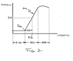
- FIG. 2 illustrates a generalized L-I curve 200 for an optical assembly.
- An L-I curve is a technique for characterizing the performance of a laser.
- the laser output power (L) can be plotted as a function of an electrical current (I) being passed through the optical assembly.
- I electrical current
- a current 212 through a laser characterized by L-I curve 200 produces an output power 214.
- the first region 202 of the curve is substantially flat. In this region the electrical current supplied to the laser does not result in a significant output of light from the optical assembly.
- a current threshold (Ith) is reached where the laser begins to produce a significant output light power.
- the threshold current may be highly variable between lasers of the same type and even lasers from the same manufacturing lot.
- the laser speed is proportional to ⁇ I / Ith where ⁇ I is the amount of current above the threshold current Ith.
- the slope efficiency may vary greatly from laser to laser.
- the L-I curve "rolls over" in a region 208, at current levels above the linear region 206.
- the light output is not directly proportional to the current applied.
- the roll-over region may also be characterized by undesirable laser characteristics including jitter (small variations in the emitted light waveform), shorter life, unstable power output, slower reaction time and distortion of the eye diagram (the viewing of multiple waveforms superimposed upon each other and may provide a subjective measure of the variations in the waveform, for example, jitter).
- FIG. 3 illustrates three L-I curves 302, 304, 320 representing three lasers, L1, L2 and L3, respectively, which may have been selected from a lot of lasers received from a supplier.
- the lasers may be specified to operate so that a laser output power is in a desired range of values 324 between a lower limit and an upper limit. A target laser power within the output range may be determined. Lasers in the lot are biased to achieve the target laser power. Because L1, L2 and L3 may have different L-I curves, the biasing requirements of the lasers may be different to achieve a similar output power.
- laser L1 requires a smaller current I 31 in order to achieve the same laser target output power as laser L2 which requires a current I 32 .
- Laser L3 may be required to operate in the roll-over region 322 operating at a current I 33 .
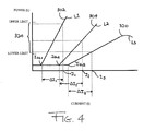
- FIG. 4 illustrates a method of tuning the laser bias.
- the laser bias may be set after the laser is installed into the optical assembly. It is assumed that the lasers do not need to meet the same target output power. Instead, the bias of each laser is set to achieve a power that is within the optical assembly specification with a ⁇ I large enough for adequate laser speed and within the roll-off region.
- the laser power is set so that the optical assembly output power is within the desired output range 324 after the laser is installed in the optical assembly.
- laser L1 is biased at a current I 1 which is ⁇ I 1 above the L1 threshold current (Ith1). That current is large enough for improved laser speed compared to FIG. 3.
- a laser having the L-I curve of L2 may be biased at a current I 2 which is ⁇ I 2 above the L2 threshold current (I th2 ) to provide an output power within the desired output range.
- the optical assembly may be designed to source less current than if the bias were set to achieve the target output power illustrated in FIG. 3.
- the bias current I 2 (FIG. 4) is lower than the bias current I 2 (FIG. 3) corresponding to the target power output.
- a laser having the L-I curve of L3 may be biased at a current I 3 which is ⁇ I 3 above the L3 threshold current (I th3 ) to provide an output power within the desired output range.
- the laser can provide the desired output at an adequate speed without operating in the roll-over region 322 of the L-I curve 320.
- the current ⁇ I x may be determined from the magnitude of the threshold current (I thx ) of a particular laser used in an optical assembly.
- Fiber optic transmitter performance may be characterized by key parameters including, but not limited to, jitter mask margin and power output. These parameters may be affected by a DC bias applied to the laser diode.
- a preferred DC bias may be used to select a preferred jitter, mask margin performance and power requirement for a particular laser.
- the preferred DC bias setting bias setting may differ for each laser type - vertical-cavity surface-emitting laser (VCSEL), Fabry-Perot (FP) laser or a distributed feed-back (DFB) laser - and may vary even within the same laser type.
- the DC bias setting may also vary for the same laser type supplied by different vendors.
- the preferred DC bias laser setting for a particular laser may be selected as a derivative of the threshold current (I th ) of the particular laser.
- Equation 2 describes a relationship where the preferred bias is a fixed multiple of the threshold current of the laser.
- the value of "k" may be determined experimentally and may be substantially constant for lasers of a particular type from the same lot.
- the current ⁇ I may be determined from a combination of the threshold current (Ith) and slope efficiency (SE) of the laser.
- the current ⁇ I can be set to a percentage of the threshold current (I th ) plus a percentage of the slope efficiency.
- Other combinations of the threshold current (I th ) and slope efficiency (SE) may be used as well.
- I opt I th * k + SE * y
- the value of where "k” and "y” may be determined experimentally and may be substantially constant for lasers of a particular type from the same vendor.
- the current ⁇ I may be determined from a combination of the threshold current (I th ), slope efficiency (SE) and the roll-over current of the L-I curve.
- Eq. 1 was applied to Honeywell 850 nanometer (nm) implant VCSELs used in the manufacturing of Finisar Corporation's (Sunnyvale, CA) FTRJ-85XX-7D-XX product family of transceivers.
- a value of "x" was determined as follows:
- Table 1 The data collected for the Honeywell 850nm implant VCSEL is shown in Table 1.
- Table 1 Current above I th (m)A Jitter (ps) Mask Margin (%) Power (dBm) 3mA 53.3 38 -7.81 5mA 35.6 47 -5.91 7mA 37.8 45 -4.81 9mA 51.1 32 -3.64
- the laser bias was set to 7.5mA above I th for the Mitsubishi 1310 FP laser used in Finisar Corporation's FTRJ-13XX-7D-XX transceiver products.
- Eq. 2 may be applied for determining the bias current levels for Honeywell 850nm oxide VCSELs.
- Various features of the system can be implemented in hardware, software, or a combination of hardware and software.
- some aspects of the system can be implemented in computer programs executing on programmable computers. Each program can be implemented in a high level procedural or object-oriented programming language to communicate with a computer system.
- each such computer program can be stored on a storage medium, such as read-only-memory (ROM), readable by a general or special purpose programmable computer, for configuring and operating the computer when the storage medium is read by the computer to perform the functions described above.
- ROM read-only-memory
Landscapes
- Physics & Mathematics (AREA)
- Condensed Matter Physics & Semiconductors (AREA)
- General Physics & Mathematics (AREA)
- Electromagnetism (AREA)
- Optics & Photonics (AREA)
- Semiconductor Lasers (AREA)
- Crystals, And After-Treatments Of Crystals (AREA)
- Optical Communication System (AREA)
Claims (11)
- Verfahren zum Einstellen eines Vorspannungsstroms für Laser, die in Laserbaugruppen (100) verwendet werden, wobei das Verfahren folgendes umfasst:a. Auswählen einer Gruppe von Stichproben von Sende-Empfängern (Transceivern) aus einem Fertigungslos, wobei die ausgewählte Gruppe repräsentativ für das ganze Fertigungslos ist;b. Bestimmen eines Schwellenstroms Ith eines Lasers, der in der ersten Transceiver-Stichprobe verwendet wird;c. Verwenden eines Vorspannungsgleichstroms zum Einrichten des Lasers in der ersten Transceiver-Stichprobe, wobei der Vorspannungsgleichstrom den Schwellenstrom Ith um einen festgelegten Betrag übersteigt;d. Einstellen eines Extinktionsverhältnisses nach Festlegung für die erste Transceiver-Stichprobe;e. Messen und Aufzeichnen eines Jitters, eines Maskenrandes und einer Leistung für die erste Transceiver-Stichprobe;f. Wiederholen von c. bis e. für die erste Transceiver-Stichprobe unter Verwendung von aufeinander folgenden höheren Vorspannungsströmen größer als Ith, bis eine bevorzugte Laser- Vorspannungsstromeinstellung überschritten ist;g. Wiederholen von c. bis f. für jede der restlichen Transceiver-Stichproben der Gruppe und Messen und Aufzeichnen einer bevorzugten Stromeinstellung oberhalb von Ith für jede übrig bleibende Transceiver-Stichprobe;h. Bestimmen eines Wertes "x" als Durchschnitt der bevorzugten Vorspannungsströme oberhalb von Ith für alle Transceiver-Stichproben der Gruppe; undi. Verwenden der folgenden Gleichung (Eq.1) zum Bestimmen des bevorzugten Vorspannungsstroms für jede Transceiver-Stichprobe des gesamten Fertigungsloses:Iopt = Ith + x, wobei Iopt der bevorzugte Vorspannungsstrom ist und Ith der Schwellenstrom für einen bestimmten Laser ist.
- Verfahren nach Anspruch 1, das das Installieren des Lasers in einer Laserbaugruppe umfasst.
- Verfahren nach Anspruch 1, das das Installieren des Lasers in einem optischen Empfänger oder optischen Transceiver umfasst.
- Verfahren nach Anspruch 1, wobei ein Satz von computerausführbaren Befehlen, die auf einem computerlesbaren Medium gespeichert sind, das Verfahren ausführt, wenn ein Computersystem nach diesen computerausführbaren Befehlen arbeitet.
- Verfahren nach Anspruch 1, wobei die Laser im Test aus der Gruppe bestehend aus VCSEL-Lasern, Fabry-Perot (FP)-Lasern oder Distributed Feedback (DFB)-Lasern ausgewählt sind.
- Verfahren nach Anspruch 1, wobei ein Laser-Vorspannungsstrom, der den bevorzugten Laser-Vorspannungsstrom übersteigt, durch eines der folgenden bestimmt wird:ein Anstieg des Jitters über einen festgelegten akzeptablen Grenzwert hinaus;eine Verringerung im Maskenrand unter einen festgelegten akzeptablen Grenzwert; odereine Veränderung der Laserausgangsleistung aus einem festgelegten akzeptablen Bereich heraus.
- Verfahren zum Einstellen eines Vorspannungsstroms für Laser, die in Laserbaugruppen (100) verwendet werden, wobei das Verfahren umfasst:a. Auswählen einer Gruppe von Stichproben von Transceivern aus einem Fertigungslos, wobei die ausgewählte Gruppe repräsentativ für das ganze Fertigungslos ist;b. Bestimmen eines Schwellenstroms Ith eines Lasers, der in einer ersten Transceiver-Stichprobe verwendet wird;c. Multiplizieren von Ith mit einem ersten "k"-Wert, um einen Einrichtungs-Vorspannungsstrom für die erste Transceiver-Stichprobe zu erhalten;d. Einstellen eines Extinktionsverhältnisses nach Festlegung für die erste Transceiver-Stichprobe;e. Messen und Aufzeichnen eines Jitters, eines Maskenrandes und einer Leistung für die erste Transceiver-Stichprobe;f. Wiederholen von c. bis e. unter Verwendung von aufeinander folgenden höheren "k"-Werten, bis eine bevorzugte Laser-Vorspannungsstromeinstellung überschritten ist;g. Wiederholen von c. bis f. für jede restliche Transceiver-Stichprobe und Messen und Aufzeichnen des bevorzugten "k"-Wertes für jede Transceiver-Stichprobe;h. Bestimmen eines "k"-Wertes für das gesamte Fertigungslos durch Mitteln der bevorzugten "k"-Werte aller Transceiver-Stichproben der Gruppe; undi. Verwenden der folgenden Gleichung (Eq.2) zum Bestimmen des bevorzugten Vorspannungsstroms für jede Transceiver-Stichprobe des gesamten Fertigungsloses:Iopt = Ith*k, wobei Iopt der bevorzugte Vorspannungsstrom ist, Ith der Schwellenstrom für einen bestimmten Laser ist und k der "k"-Wert für das gesamte Fertigungslos ist.
- Verfahren wie in Anspruch 7 angegeben, wobei ein Satz von computerausführbaren Befehlen, die auf einem computerlesbaren Medium gespeichert sind, das Verfahren ausführt, wenn ein Computersystem nach diesen computerausführbaren Befehlen arbeitet.
- Verfahren nach Anspruch 7, wobei die Laser im Test aus der Gruppe bestehend aus VCSEL-Lasern, Fabry-Perot (FP)-Lasern oder Distributed Feedback (DFB)-Lasern ausgewählt sind.
- Verfahren nach Anspruch 7, wobei der erste "k"-Wert 2,0 ist.
- Verfahren nach Anspruch 7, wobei das Verfahren in Verbindung mit einem Fertigungslos von 850 nm-Oxid-VCSEL-Lasern ausgeführt wird.
Applications Claiming Priority (5)
| Application Number | Priority Date | Filing Date | Title |
|---|---|---|---|
| US38245502P | 2002-05-22 | 2002-05-22 | |
| US382455P | 2002-05-22 | ||
| US10/228,563 US6873632B2 (en) | 2002-05-22 | 2002-08-27 | Techniques for biasing lasers |
| US228563 | 2002-08-27 | ||
| PCT/US2003/012800 WO2003100927A1 (en) | 2002-05-22 | 2003-04-24 | Techniques for biasing lasers |
Publications (3)
| Publication Number | Publication Date |
|---|---|
| EP1509977A1 EP1509977A1 (de) | 2005-03-02 |
| EP1509977A4 EP1509977A4 (de) | 2005-08-17 |
| EP1509977B1 true EP1509977B1 (de) | 2007-02-28 |
Family
ID=29552885
Family Applications (1)
| Application Number | Title | Priority Date | Filing Date |
|---|---|---|---|
| EP03728529A Expired - Lifetime EP1509977B1 (de) | 2002-05-22 | 2003-04-24 | Techniken zur vorspannung von lasern |
Country Status (7)
| Country | Link |
|---|---|
| US (1) | US6873632B2 (de) |
| EP (1) | EP1509977B1 (de) |
| AT (1) | ATE355641T1 (de) |
| AU (1) | AU2003234219A1 (de) |
| DE (1) | DE60312157T2 (de) |
| MY (1) | MY141492A (de) |
| WO (1) | WO2003100927A1 (de) |
Families Citing this family (9)
| Publication number | Priority date | Publication date | Assignee | Title |
|---|---|---|---|---|
| US7120179B2 (en) * | 2002-11-08 | 2006-10-10 | Finisar Corporation | Apparatus and method for setting AC bias point of an optical transmitter module in an optoelectronic transceiver |
| KR100532309B1 (ko) * | 2003-04-21 | 2005-11-29 | 삼성전자주식회사 | 외부 온도변화와 무관하게 페브리-페롯 레이저의파장잠김을 유지하는 방법 및 이를 이용한파장분할다중방식 광원 |
| JP4574650B2 (ja) * | 2007-07-09 | 2010-11-04 | キヤノン株式会社 | レーザダイオード駆動装置及び光走査装置 |
| JP5362301B2 (ja) * | 2008-09-19 | 2013-12-11 | 株式会社Qdレーザ | レーザシステム |
| US9735879B2 (en) | 2014-09-30 | 2017-08-15 | International Business Machines Corporation | Near-threshold optical transmitter pre-distortion |
| CN105610048A (zh) * | 2016-03-23 | 2016-05-25 | 青岛海信宽带多媒体技术有限公司 | 光模块生产方法和装置、光模块驱动方法和光模块 |
| US11949453B2 (en) * | 2021-06-25 | 2024-04-02 | Electronics And Telecommunications Research Institute | Test device and test method for DFB-LD for RoF system |
| EP4439883A1 (de) * | 2023-03-29 | 2024-10-02 | Honeywell International Inc. | Laserkalibrierungs- und -stabilisierungsalgorithmus für eine mikroskopievorrichtung |
| CN121750105A (zh) * | 2024-09-26 | 2026-03-27 | 锐捷网络股份有限公司 | 参数确定方法、通信方法、装置、电子设备及存储介质 |
Family Cites Families (9)
| Publication number | Priority date | Publication date | Assignee | Title |
|---|---|---|---|---|
| US5140603A (en) * | 1990-05-02 | 1992-08-18 | Scientific-Atlanta, Inc. | Overmodulation protection for amplitude modulated laser diode |
| US5019769A (en) * | 1990-09-14 | 1991-05-28 | Finisar Corporation | Semiconductor laser diode controller and laser diode biasing control method |
| JPH05244097A (ja) * | 1992-02-12 | 1993-09-21 | Nec Corp | E/oアレイの駆動方式 |
| US5812572A (en) * | 1996-07-01 | 1998-09-22 | Pacific Fiberoptics, Inc. | Intelligent fiberoptic transmitters and methods of operating and manufacturing the same |
| JP3700296B2 (ja) * | 1996-11-29 | 2005-09-28 | 富士ゼロックス株式会社 | 半導体レーザ駆動装置および画像記録装置 |
| JPH11135871A (ja) * | 1997-10-28 | 1999-05-21 | Nec Corp | レーザダイオード駆動方法および回路 |
| JP4026918B2 (ja) * | 1998-03-02 | 2007-12-26 | キヤノン株式会社 | レーザ駆動装置およびその制御方法 |
| US6055252A (en) * | 1998-09-10 | 2000-04-25 | Photonic Solutions, Inc. | Fiberoptic transmitter using thermistor to maintain stable operating conditions over a range of temperature |
| US6771679B2 (en) * | 2000-05-17 | 2004-08-03 | David Chalmers Schie | Apparatus and method for programmable control of laser diode modulation and operating point |
-
2002
- 2002-08-27 US US10/228,563 patent/US6873632B2/en not_active Expired - Lifetime
-
2003
- 2003-04-24 EP EP03728529A patent/EP1509977B1/de not_active Expired - Lifetime
- 2003-04-24 DE DE60312157T patent/DE60312157T2/de not_active Expired - Lifetime
- 2003-04-24 WO PCT/US2003/012800 patent/WO2003100927A1/en not_active Ceased
- 2003-04-24 AT AT03728529T patent/ATE355641T1/de not_active IP Right Cessation
- 2003-04-24 AU AU2003234219A patent/AU2003234219A1/en not_active Abandoned
- 2003-05-06 MY MYPI20031708A patent/MY141492A/en unknown
Also Published As
| Publication number | Publication date |
|---|---|
| ATE355641T1 (de) | 2006-03-15 |
| MY141492A (en) | 2010-04-30 |
| AU2003234219A1 (en) | 2003-12-12 |
| EP1509977A4 (de) | 2005-08-17 |
| WO2003100927A1 (en) | 2003-12-04 |
| DE60312157D1 (de) | 2007-04-12 |
| US6873632B2 (en) | 2005-03-29 |
| DE60312157T2 (de) | 2007-11-29 |
| US20030219051A1 (en) | 2003-11-27 |
| EP1509977A1 (de) | 2005-03-02 |
Similar Documents
| Publication | Publication Date | Title |
|---|---|---|
| US6947455B2 (en) | Maintaining desirable performance of optical emitters at extreme temperatures | |
| US7386020B2 (en) | Systems, devices and methods for temperature-based control of laser performance | |
| US4612671A (en) | Laser transmitter | |
| US7269191B2 (en) | Control circuit for optoelectronic module with integrated temperature control | |
| US6795458B2 (en) | Laser diode control circuit and laser diode control method | |
| US7236507B2 (en) | Time-based adjustment of temperature control of laser to stabilize wavelengths | |
| WO1998000893A1 (en) | Intelligent fiberoptic transmitters and methods of operating and manufacturing the same | |
| US20040264523A1 (en) | Temperature compensation circuit to maintain ratio of monitor photodiode current to fiber coupled light in a laser | |
| EP1480358B1 (de) | Optisches übertragungsmodul mit digitaler einstellung und einstellverfahren | |
| US7639952B2 (en) | Calculation of laser slope efficiency in an optical transceiver module | |
| US20060062116A1 (en) | Optical data link capable of compensating tracking error | |
| US7850083B2 (en) | Digital control system for an electro-optical device | |
| JP5007015B2 (ja) | レーザシステムを制御及び較正する方法及びシステム | |
| US6873632B2 (en) | Techniques for biasing lasers | |
| JP2013175517A (ja) | 光データリンクの製造方法 | |
| US6947457B2 (en) | DFB laser driving device, DFB laser driving method and storage medium | |
| EP1167943A2 (de) | Feststellung der Alterung von optischen Komponenten | |
| Jewell et al. | 1310nm VCSELs in 1-10Gb/s commercial applications | |
| CA2504691C (en) | Age compensation in optoelectronic modules with integrated temperature control | |
| US7058099B2 (en) | Age compensation in optoelectronic modules with integrated temperature control | |
| CA2327981A1 (en) | A method and apparatus to select optimal operating conditions in a digital wavelength stabilized control system | |
| US20020163945A1 (en) | Modulation current compensation of laser for controlled extinction ratio using dither signal | |
| EP1485736B1 (de) | Aufrechterhalten einer erwünschten Leistungsfähigkeit optischer Emitter bei extremen Temperaturen | |
| US20030113058A1 (en) | Control system for dynamic gain equalization filter | |
| US6441940B1 (en) | Wavelength stabilization of light emitting components |
Legal Events
| Date | Code | Title | Description |
|---|---|---|---|
| PUAI | Public reference made under article 153(3) epc to a published international application that has entered the european phase |
Free format text: ORIGINAL CODE: 0009012 |
|
| 17P | Request for examination filed |
Effective date: 20041220 |
|
| AK | Designated contracting states |
Kind code of ref document: A1 Designated state(s): AT BE BG CH CY CZ DE DK EE ES FI FR GB GR HU IE IT LI LU MC NL PT RO SE SI SK TR |
|
| AX | Request for extension of the european patent |
Extension state: AL LT LV MK |
|
| A4 | Supplementary search report drawn up and despatched |
Effective date: 20050705 |
|
| RIC1 | Information provided on ipc code assigned before grant |
Ipc: 7H 01S 5/062 B Ipc: 7H 01S 5/068 A |
|
| GRAP | Despatch of communication of intention to grant a patent |
Free format text: ORIGINAL CODE: EPIDOSNIGR1 |
|
| GRAS | Grant fee paid |
Free format text: ORIGINAL CODE: EPIDOSNIGR3 |
|
| GRAA | (expected) grant |
Free format text: ORIGINAL CODE: 0009210 |
|
| RAP1 | Party data changed (applicant data changed or rights of an application transferred) |
Owner name: FINISAR CORPORATION |
|
| AK | Designated contracting states |
Kind code of ref document: B1 Designated state(s): AT BE BG CH CY CZ DE DK EE ES FI FR GB GR HU IE IT LI LU MC NL PT RO SE SI SK TR |
|
| AX | Request for extension of the european patent |
Extension state: AL LT LV MK |
|
| PG25 | Lapsed in a contracting state [announced via postgrant information from national office to epo] |
Ref country code: FI Free format text: LAPSE BECAUSE OF FAILURE TO SUBMIT A TRANSLATION OF THE DESCRIPTION OR TO PAY THE FEE WITHIN THE PRESCRIBED TIME-LIMIT Effective date: 20070228 Ref country code: BE Free format text: LAPSE BECAUSE OF FAILURE TO SUBMIT A TRANSLATION OF THE DESCRIPTION OR TO PAY THE FEE WITHIN THE PRESCRIBED TIME-LIMIT Effective date: 20070228 Ref country code: LI Free format text: LAPSE BECAUSE OF FAILURE TO SUBMIT A TRANSLATION OF THE DESCRIPTION OR TO PAY THE FEE WITHIN THE PRESCRIBED TIME-LIMIT Effective date: 20070228 Ref country code: DK Free format text: LAPSE BECAUSE OF FAILURE TO SUBMIT A TRANSLATION OF THE DESCRIPTION OR TO PAY THE FEE WITHIN THE PRESCRIBED TIME-LIMIT Effective date: 20070228 Ref country code: CH Free format text: LAPSE BECAUSE OF FAILURE TO SUBMIT A TRANSLATION OF THE DESCRIPTION OR TO PAY THE FEE WITHIN THE PRESCRIBED TIME-LIMIT Effective date: 20070228 Ref country code: NL Free format text: LAPSE BECAUSE OF FAILURE TO SUBMIT A TRANSLATION OF THE DESCRIPTION OR TO PAY THE FEE WITHIN THE PRESCRIBED TIME-LIMIT Effective date: 20070228 Ref country code: AT Free format text: LAPSE BECAUSE OF FAILURE TO SUBMIT A TRANSLATION OF THE DESCRIPTION OR TO PAY THE FEE WITHIN THE PRESCRIBED TIME-LIMIT Effective date: 20070228 Ref country code: SI Free format text: LAPSE BECAUSE OF FAILURE TO SUBMIT A TRANSLATION OF THE DESCRIPTION OR TO PAY THE FEE WITHIN THE PRESCRIBED TIME-LIMIT Effective date: 20070228 |
|
| REG | Reference to a national code |
Ref country code: GB Ref legal event code: FG4D |
|
| REG | Reference to a national code |
Ref country code: CH Ref legal event code: EP |
|
| REF | Corresponds to: |
Ref document number: 60312157 Country of ref document: DE Date of ref document: 20070412 Kind code of ref document: P |
|
| REG | Reference to a national code |
Ref country code: IE Ref legal event code: FG4D |
|
| PG25 | Lapsed in a contracting state [announced via postgrant information from national office to epo] |
Ref country code: BG Free format text: LAPSE BECAUSE OF EXPIRATION OF PROTECTION Effective date: 20070529 |
|
| PG25 | Lapsed in a contracting state [announced via postgrant information from national office to epo] |
Ref country code: SE Free format text: LAPSE BECAUSE OF FAILURE TO SUBMIT A TRANSLATION OF THE DESCRIPTION OR TO PAY THE FEE WITHIN THE PRESCRIBED TIME-LIMIT Effective date: 20070531 |
|
| PG25 | Lapsed in a contracting state [announced via postgrant information from national office to epo] |
Ref country code: ES Free format text: LAPSE BECAUSE OF FAILURE TO SUBMIT A TRANSLATION OF THE DESCRIPTION OR TO PAY THE FEE WITHIN THE PRESCRIBED TIME-LIMIT Effective date: 20070608 |
|
| PG25 | Lapsed in a contracting state [announced via postgrant information from national office to epo] |
Ref country code: PT Free format text: LAPSE BECAUSE OF FAILURE TO SUBMIT A TRANSLATION OF THE DESCRIPTION OR TO PAY THE FEE WITHIN THE PRESCRIBED TIME-LIMIT Effective date: 20070730 |
|
| NLV1 | Nl: lapsed or annulled due to failure to fulfill the requirements of art. 29p and 29m of the patents act | ||
| ET | Fr: translation filed | ||
| LTIE | Lt: invalidation of european patent or patent extension |
Effective date: 20070228 |
|
| REG | Reference to a national code |
Ref country code: CH Ref legal event code: PL |
|
| PG25 | Lapsed in a contracting state [announced via postgrant information from national office to epo] |
Ref country code: SK Free format text: LAPSE BECAUSE OF FAILURE TO SUBMIT A TRANSLATION OF THE DESCRIPTION OR TO PAY THE FEE WITHIN THE PRESCRIBED TIME-LIMIT Effective date: 20070228 |
|
| PG25 | Lapsed in a contracting state [announced via postgrant information from national office to epo] |
Ref country code: RO Free format text: LAPSE BECAUSE OF FAILURE TO SUBMIT A TRANSLATION OF THE DESCRIPTION OR TO PAY THE FEE WITHIN THE PRESCRIBED TIME-LIMIT Effective date: 20070228 Ref country code: CZ Free format text: LAPSE BECAUSE OF FAILURE TO SUBMIT A TRANSLATION OF THE DESCRIPTION OR TO PAY THE FEE WITHIN THE PRESCRIBED TIME-LIMIT Effective date: 20070228 |
|
| PLBE | No opposition filed within time limit |
Free format text: ORIGINAL CODE: 0009261 |
|
| STAA | Information on the status of an ep patent application or granted ep patent |
Free format text: STATUS: NO OPPOSITION FILED WITHIN TIME LIMIT |
|
| 26N | No opposition filed |
Effective date: 20071129 |
|
| PG25 | Lapsed in a contracting state [announced via postgrant information from national office to epo] |
Ref country code: IT Free format text: LAPSE BECAUSE OF FAILURE TO SUBMIT A TRANSLATION OF THE DESCRIPTION OR TO PAY THE FEE WITHIN THE PRESCRIBED TIME-LIMIT Effective date: 20070228 Ref country code: GR Free format text: LAPSE BECAUSE OF FAILURE TO SUBMIT A TRANSLATION OF THE DESCRIPTION OR TO PAY THE FEE WITHIN THE PRESCRIBED TIME-LIMIT Effective date: 20070529 |
|
| PG25 | Lapsed in a contracting state [announced via postgrant information from national office to epo] |
Ref country code: IE Free format text: LAPSE BECAUSE OF NON-PAYMENT OF DUE FEES Effective date: 20070424 |
|
| PG25 | Lapsed in a contracting state [announced via postgrant information from national office to epo] |
Ref country code: EE Free format text: LAPSE BECAUSE OF FAILURE TO SUBMIT A TRANSLATION OF THE DESCRIPTION OR TO PAY THE FEE WITHIN THE PRESCRIBED TIME-LIMIT Effective date: 20070228 |
|
| PG25 | Lapsed in a contracting state [announced via postgrant information from national office to epo] |
Ref country code: MC Free format text: LAPSE BECAUSE OF NON-PAYMENT OF DUE FEES Effective date: 20070430 |
|
| PG25 | Lapsed in a contracting state [announced via postgrant information from national office to epo] |
Ref country code: CY Free format text: LAPSE BECAUSE OF FAILURE TO SUBMIT A TRANSLATION OF THE DESCRIPTION OR TO PAY THE FEE WITHIN THE PRESCRIBED TIME-LIMIT Effective date: 20070228 |
|
| PG25 | Lapsed in a contracting state [announced via postgrant information from national office to epo] |
Ref country code: LU Free format text: LAPSE BECAUSE OF NON-PAYMENT OF DUE FEES Effective date: 20070424 |
|
| PG25 | Lapsed in a contracting state [announced via postgrant information from national office to epo] |
Ref country code: HU Free format text: LAPSE BECAUSE OF FAILURE TO SUBMIT A TRANSLATION OF THE DESCRIPTION OR TO PAY THE FEE WITHIN THE PRESCRIBED TIME-LIMIT Effective date: 20070901 Ref country code: TR Free format text: LAPSE BECAUSE OF FAILURE TO SUBMIT A TRANSLATION OF THE DESCRIPTION OR TO PAY THE FEE WITHIN THE PRESCRIBED TIME-LIMIT Effective date: 20070228 |
|
| PGFP | Annual fee paid to national office [announced via postgrant information from national office to epo] |
Ref country code: GB Payment date: 20140428 Year of fee payment: 12 |
|
| PGFP | Annual fee paid to national office [announced via postgrant information from national office to epo] |
Ref country code: FR Payment date: 20140417 Year of fee payment: 12 Ref country code: DE Payment date: 20140429 Year of fee payment: 12 |
|
| REG | Reference to a national code |
Ref country code: DE Ref legal event code: R119 Ref document number: 60312157 Country of ref document: DE |
|
| GBPC | Gb: european patent ceased through non-payment of renewal fee |
Effective date: 20150424 |
|
| PG25 | Lapsed in a contracting state [announced via postgrant information from national office to epo] |
Ref country code: DE Free format text: LAPSE BECAUSE OF NON-PAYMENT OF DUE FEES Effective date: 20151103 Ref country code: GB Free format text: LAPSE BECAUSE OF NON-PAYMENT OF DUE FEES Effective date: 20150424 |
|
| REG | Reference to a national code |
Ref country code: FR Ref legal event code: ST Effective date: 20151231 |
|
| PG25 | Lapsed in a contracting state [announced via postgrant information from national office to epo] |
Ref country code: FR Free format text: LAPSE BECAUSE OF NON-PAYMENT OF DUE FEES Effective date: 20150430 |