EP1509996B1 - Aufwärts-frequenzumsetzer - Google Patents
Aufwärts-frequenzumsetzer Download PDFInfo
- Publication number
- EP1509996B1 EP1509996B1 EP03732897A EP03732897A EP1509996B1 EP 1509996 B1 EP1509996 B1 EP 1509996B1 EP 03732897 A EP03732897 A EP 03732897A EP 03732897 A EP03732897 A EP 03732897A EP 1509996 B1 EP1509996 B1 EP 1509996B1
- Authority
- EP
- European Patent Office
- Prior art keywords
- frequency converter
- accordance
- control
- control elements
- input
- Prior art date
- Legal status (The legal status is an assumption and is not a legal conclusion. Google has not performed a legal analysis and makes no representation as to the accuracy of the status listed.)
- Expired - Lifetime
Links
- 239000000758 substrate Substances 0.000 claims abstract description 10
- 239000004020 conductor Substances 0.000 claims description 32
- 239000003990 capacitor Substances 0.000 description 7
- 238000010586 diagram Methods 0.000 description 3
- 230000005540 biological transmission Effects 0.000 description 2
- 238000004891 communication Methods 0.000 description 2
- 238000004519 manufacturing process Methods 0.000 description 2
- 229910001218 Gallium arsenide Inorganic materials 0.000 description 1
- 241000233805 Phoenix Species 0.000 description 1
- 239000000654 additive Substances 0.000 description 1
- 230000000996 additive effect Effects 0.000 description 1
- 238000006243 chemical reaction Methods 0.000 description 1
- 230000001419 dependent effect Effects 0.000 description 1
- 230000009977 dual effect Effects 0.000 description 1
- 238000005516 engineering process Methods 0.000 description 1
- 230000010354 integration Effects 0.000 description 1
- 238000000034 method Methods 0.000 description 1
- 239000004065 semiconductor Substances 0.000 description 1
- 230000003595 spectral effect Effects 0.000 description 1
Images


Classifications
-
- H—ELECTRICITY
- H03—ELECTRONIC CIRCUITRY
- H03D—DEMODULATION OR TRANSFERENCE OF MODULATION FROM ONE CARRIER TO ANOTHER
- H03D7/00—Transference of modulation from one carrier to another, e.g. frequency-changing
- H03D7/14—Balanced arrangements
- H03D7/1425—Balanced arrangements with transistors
- H03D7/1441—Balanced arrangements with transistors using field-effect transistors
-
- H—ELECTRICITY
- H03—ELECTRONIC CIRCUITRY
- H03D—DEMODULATION OR TRANSFERENCE OF MODULATION FROM ONE CARRIER TO ANOTHER
- H03D7/00—Transference of modulation from one carrier to another, e.g. frequency-changing
- H03D7/14—Balanced arrangements
- H03D7/1425—Balanced arrangements with transistors
- H03D7/1458—Double balanced arrangements, i.e. where both input signals are differential
-
- H—ELECTRICITY
- H03—ELECTRONIC CIRCUITRY
- H03D—DEMODULATION OR TRANSFERENCE OF MODULATION FROM ONE CARRIER TO ANOTHER
- H03D7/00—Transference of modulation from one carrier to another, e.g. frequency-changing
- H03D7/14—Balanced arrangements
- H03D7/1425—Balanced arrangements with transistors
- H03D7/1466—Passive mixer arrangements
-
- H—ELECTRICITY
- H03—ELECTRONIC CIRCUITRY
- H03D—DEMODULATION OR TRANSFERENCE OF MODULATION FROM ONE CARRIER TO ANOTHER
- H03D2200/00—Indexing scheme relating to details of demodulation or transference of modulation from one carrier to another covered by H03D
- H03D2200/0001—Circuit elements of demodulators
- H03D2200/0023—Balun circuits
-
- H—ELECTRICITY
- H03—ELECTRONIC CIRCUITRY
- H03D—DEMODULATION OR TRANSFERENCE OF MODULATION FROM ONE CARRIER TO ANOTHER
- H03D2200/00—Indexing scheme relating to details of demodulation or transference of modulation from one carrier to another covered by H03D
- H03D2200/0041—Functional aspects of demodulators
- H03D2200/0043—Bias and operating point
Definitions
- the present invention relates to an up-frequency converter.
- Such frequency converters are required in radio communication systems for shifting a message signal present with an intermediate frequency to a transmission frequency provided for the radio transmission.
- the wavelengths of the radio signals can be in the millimeter range.
- An up-frequency converter according to the preamble of claim 1 is made Nishikawa et al., "Broadband and Compact SiBJT Balanced Up Converter MMIC using Si3-D MMIC Technology", IEEE MMT-S International Microwave Symposium 2001, Phoenix, Arizona, USA, pp. 87-90 ,
- this known frequency converter the two signals to be mixed, an intermediate frequency signal and a local oscillator signal, respectively in push-pull at the bases of two bipolar transistors and modulate currents flowing through the bipolar transistors, the additive are superimposed to be issued high frequency signal.
- the anti-phase local oscillator signals applied to the bipolar transistors are supplied by a balun integrated on the substrate, to the input of which the local oscillator signal is fed in asymmetric form.
- the Symmetriergl ied is composed of a plurality of conductor track sections, each with .. a length ⁇ / 4 and occupied on the substrate of the integrated circuit more space than all the other circuit components together.
- the intermediate frequency signal which is also required in symmetrical form and whose frequency is lower than that of the local oscillator signal, is supplied to the circuit via two separate connections from the outside. Differences in the lines lying outside the integrated circuit to these two terminals, in particular different lengths and attenuations, can lead to different amplitudes of the applied intermediate frequency signals and deviations of their phase difference from the desired exact antiphase and thus to an asymmetry in the behavior of the two bipolar transistors.
- the quality of the mixing result thus depends inter alia on the wiring of the circuit; ie wiring manufacturing issues can affect the efficiency of the frequency converter.
- a down-converter realized in a monolithic microwave integrated circuit is known in which a balun connected to the lower frequency input of the mixer is used.
- the object of the present invention is to provide an integratable up-frequency converter with a good, reproducible and little dependent on manufacturing scattering conversion behavior.
- the object is achieved by an up-frequency converter with the features of claim 1.
- a third control element whose control terminal is connected to the first input signal and whose two main terminals are each connected to one of two supply potentials of the up-frequency converter and one terminal of the first and second control element is used as balun for the lower input frequency.
- a balun requires very little substrate area compared to a balun of Nishikawa et al. type, the space required is proportional to the wavelength of the signal to be balanced, and it has a large bandwidth.
- the terminals of the first and second control elements, respectively, to which the main terminals of the third control element are connected are respectively their second main terminals. This allows a multiplicative modulation of the first input signal by the second and thus a high efficiency of the mixing process.
- transistors in particular HEMTs (High Electron Mobility Transistors) are used.
- the first and second controls are preferably biased to near their pinch-off region.
- a balancing member is also provided for the second, higher-frequency input signal, which is connected on the output side to the control inputs of the first and the second control element.
- the invention also relates to a single-sideband frequency converter, which can be realized from the above-described up-frequency converters by the outputs of two such up-frequency converter are connected to inputs of a Lange coupler, of which an output forms the output of the single-sideband frequency converter.
- the second balun of the up-frequency converter of such a single-sideband frequency converter expediently fused to a power divider to save substrate area.
- the power divider distributes the second input signal equally to the two up-frequency converters.
- Such a fused or combined balun is simple and space-saving feasible with a central, connected to a signal input of the single sideband frequency converter first conductor portion and, on both sides of the first conductor portion, a plurality of second conductor portions, wherein the control inputs of the first and second control of the first Up-frequency converter are connected to second conductor sections on one side of the central conductor portion and the control inputs of the first and second control element of the second up-frequency converter are connected to second conductor portions on the other side of the central conductor portion.
- These conductor sections can be easily realized as microstrip conductors in a common plane.
- the second balancing member has three juxtaposed conductor sections on both sides of the central conductor section, of which in each case a middle is unconnected.
- FIG. 12 is a schematic circuit diagram of a substrate-integrated up-frequency converter according to the present invention.
- FIG. This includes as controls two GaAs HEMTs Q1 and Q2 in a symmetrical arrangement.
- the gates of the HEMTs Q1, Q2 are connected in series with a local oscillator signal LO via a 180 ° hybrid coupler composed of parallel strip conductors S1 to S4 and capacitors C1, C2.
- the drains of the HEMTs Q1, Q2 are connected to each other and via two inductors L8, L7 to an input terminal for a supply voltage VD2.
- each HEMT Q1, Q2 is connected via a capacitor C3 or C4 with source and drain of a third HEMT Q3 and via a capacitor C5 or C6 and via a series circuit with an inductance L5 or L6 and a resistor R1 or R2 connected to ground.
- Source and drain of the HEMT Q3 are each connected via an inductance L1 and L2 to ground GND and a supply potential VD1.
- a bias voltage VG1 via an inductor L9 and the intermediate frequency signal IF via a capacitor C13.
- the voltage at the gate of the HEMT Q3 is thus composed of a DC component contributed by VG1 and an AC component contributed by IF.
- the DC component is chosen so that the HEMT Q3 works in the linear range; IF largely linearly modulates the drain current of the HEMT Q3.
- the potentials at the drain and source of the HEMT Q3 thus oscillate in phase opposition to each other with a larger amplitude than that of the IF signal.
- the HEMT Q3 thus acts simultaneously as an amplifier and as a balancing member for the intermediate frequency signal IF.
- one will select equal values of the inductors L1, L2 to achieve equal amplitudes of the intermediate frequency signal at the source and drain of the HEMT Q3.
- the current flows through the two HEMTs Q1, Q2, whose drain is applied to the supply voltage VD2 via the inductors L8, L7, are each composed mainly of a component with the frequency of the local oscillator signal LO, a component with the frequency of the intermediate frequency signal IF and components at the sum and the difference of the frequencies of local oscillator signal LO and intermediate frequency signal IF. Since the gates of the HEMTs Q1, Q2 are connected in antiphase with the local oscillator signal LO, the proportions of these current flows with the local oscillator frequency are in each case opposite and cancel each other. Likewise, the intermediate frequency components are each equal to the opposite and cancel each other.
- the current flowing through the inductance L3 and thus the potential at the connection point between the inductors L7, L8 thus contains only spectral components with the sum or difference frequency. These components are connected via a capacitor C8 to the output HF coupled and give the output of the up-frequency converter, a carrierless high frequency signal with two sidebands each formed by the sum or difference frequency component.
- Fig. 2 shows a single-sideband converter consisting of two up-converters from the in Fig. 1 shown type is composed.
- the arrangement of the two up-converters is mirror-symmetric, their components have in Fig. 2 the same reference numerals as in Fig. 1 , wherein the second mixer in Fig. 2 each marked by an apostrophe (').
- the intermediate frequency signal IF 'fed to the second mixer is phase-shifted by 90 ° with respect to the intermediate frequency signal IF.
- the output signals of the two upconverters are superimposed in a Lange coupler LC, of which two outputs then one provides the upper sideband (USB), the other the lower (LSB).
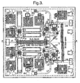
- Fig. 3 schematically shows the arrangement of the various components of the single sideband mixer Fig. 2 on a substrate.
- the two up-mixers are arranged mirror-symmetrically on both sides of a dot-dashed center line AA.
- this center line AA extends a dual balun which comprises seven parallel microstrip sections S1, S2, S3, S4, S2 ', S3', S4 '.
- a middle of these sections S1 is on one of its ends is connected to a terminal pad for the local oscillator signal LO, the other end remote from the LO terminal pad is grounded.
- this middle microstrip conductor S1 to the outside are arranged in order: a first microstrip conductor S2, S2 ', which is connected to ground at an end facing the local oscillator connection pad LO and at an opposite end via the capacitor C2 or C2' to the HEMT Q2 and Q2 ', a second microstrip S3, S3', which is connected at its local oscillator terminal pad LO end facing the corresponding end of the microstrip conductor S1 and is set at its opposite end as the microstrip conductor S1 to ground, and a third microstrip conductor S4, S4 ', which is connected at its the local oscillator pad LO end facing S1, S3, S3' and connected at its opposite end via the capacitor C1 and C1 'to the HEMT Q1 and Q1' ,
- the double balun thus simultaneously acts as a power divider which supplies the local oscillator signal LO with equal power to the two up-frequency converters on either side of the center line A-A.
Landscapes
- Engineering & Computer Science (AREA)
- Power Engineering (AREA)
- Superheterodyne Receivers (AREA)
- Transmitters (AREA)
- Stabilization Of Oscillater, Synchronisation, Frequency Synthesizers (AREA)
- Channel Selection Circuits, Automatic Tuning Circuits (AREA)
- Control Of High-Frequency Heating Circuits (AREA)
Description
- Die vorliegende Erfindung betrifft einen Aufwärts-Frequenzumsetzer. Derartige Frequenzumsetzer werden in Funk-Kommunikationssystemen zum Verschieben eines mit einer Zwischenfrequenz vorliegenden Nachrichtensignals auf eine für die Funkübertragung vorgesehene Sendefrequenz benötigt. Die Wellenlängen der Funksignale können im Millimeterbereich liegen.
- Der zunehmende Umfang der Integration bei Kommunikationssystemen für diese Wellenlängen führt auch zu einem gesteigerten Bedarf nach platzsparend monolithisch integrierbaren Frequenzumsetzern.
- Ein Aufwärts-Frequenzumsetzer nach dem Oberbegriff des Anspruchs 1 ist aus Nishikawa et al., "Broadband and Compact SiBJT Balanced Up-Converter MMIC using Si 3-D MMIC Technology", IEEE MMT-S International Microwave Symposium 2001, Phoenix, Arizona, USA, S. 87 - 90, bekannt. Bei diesem bekannten Frequenzumsetzer liegen die zwei zu mischenden Signale, ein Zwischenfrequenzsignal und ein Lokaloszillatorsignal, jeweils im Gegentakt an den Basen von zwei Bipolartransistoren an und modulieren durch die Bipolartransistoren fließende Ströme, die additiv zum auszugebenden Hochfrequenzsignal überlagert werden. Die an die Bipolartransistoren angelegten gegenphasigen Lokaloszillatorsignale werden von einem auf dem Substrat integrierten Symmetrierglied geliefert, an dessen Eingang das Lokaloszillatorsignal in asymmetrischer Form eingespeist wird. Das Symmetriergl ied ist aufgebaut aus einer Mehrzahl von Leiterbahnabschnitten mit jeweils.. einer Länge λ/4 und belegt auf dem Substrat der integrierten Schaltung mehr Platz als alle anderen Schaltungskomponenten zusammen. Das ebenfalls in symmetrischer Form benötigte Zwischenfrequenzsignal, dessen Frequenz niedriger als die des Lokaloszillatorsignals ist, wird der Schaltung über zwei getrennte Anschlüsse von außen zugeführt. Unterschiede in den außerhalb der integrierten Schaltung liegenden Zuleitungen zu diesen zwei Anschlüssen, insbesondere unterschiedliche Längen und Dämpfungen, können zu unterschiedlichen Amplituden der anliegenden Zwischenfrequenzsignale und Abweichungen ihrer Phasendifferenz von der gewünschten exakten Gegenphasigkeit und damit zu einer Asymmetrie im Verhalten der zwei Bipolartransistoren führen. Die Qualität des Mischungsergebnisses hängt somit unter anderem von der Verdrahtung der Schaltung ab; d. h. Fertigungsstreuungen bei der Verdrahtung können die Wirksamkeit des Frequenzumsetzers beeinträchtigen.
- Aus der
US 2001/0046849 A1 ist ein in einem monolithisch integrierten Mikrowellenschaltkreis (MMIC) verwirklichter Abwärtsumsetzer bekannt, bei dem ein mit dem Eingangssignal niedrigerer Frequenz des Mischers verbundenes Symmetrieglied verwendet wird. - Aufgabe der vorliegenden Erfindung ist, einen integrierbaren Aufwärts-Frequenzumsetzer mit einem guten, reproduzierbaren und von Fertigungsstreuungen wenig abhängigen Umsetzverhalten zu schaffen. Die Aufgabe wird gelöst durch einen Aufwärts-Frequenzumsetzer mit den Merkmalen des Anspruchs 1. Indem ein Symmetrierglied für die niedrigere Eingangsfrequenz auf dem Substrat integriert wird, werden Länge und Dämpfung der Verbindung zwischen dem Symmetrierglied und den ersten Hauptanschlüssen der zwei Steuerelemente exakt kontrollierbar und reproduzierbar.
- Vorzugsweise wird als Symmetrierglied für die niedrigere Eingangsfrequenz ein drittes Steuerelement eingesetzt, dessen Steueranschluss mit dem ersten Eingangssignal beschaltet ist und von dessen zwei Hauptanschlüssen jeder mit einem von zwei Versorgungspotentialen des Aufwärts-Frequenzumsetzers und einem Anschluss des ersten bzw. zweiten Steuerelementes verbunden ist. Ein solches Symmetrierglied erfordert sehr wenig Substratfläche im Vergleich zu einem Symmetrierglied des bei Nishikawa et al. eingesetzten Typs, dessen Platzbedarf proportional zur Wellenlänge des zu symmetrierenden Signals ist, und es weist eine große Bandbreite auf.
- Vorzugsweise sind die Anschlüsse des ersten bzw. zweiten Steuerelements, mit dem die Hauptanschlüsse des dritten Steuerelementes verbunden sind, jeweils deren zweite Hauptanschlüsse. Dies erlaubt eine multiplikative Modulation des ersten Eingangssignals durch das zweite und damit eine hohe Effektivität des Mischvorgangs.
- Als Steuerelemente werden vorzugsweise Transistoren, insbesondere HEMTs (High Electron Mobility Transistors) eingesetzt.
- Um eine hohe Mischungseffizienz zu erreichen, sind das erste und das zweite Steuerelement vorzugsweise bis in die Nähe ihres Pinch-off-Bereiches vorgespannt.
- Zweckmäßigerweise ist auch für das zweite, höher frequente Eingangssignal ein Symmetrierglied vorgesehen, das ausgangsseitig mit den Steuereingängen des ersten und des zweiten Steuerelements verbunden ist.
- Gegenstand der Erfindung ist ferner ein Einseitenband-Frequenzumsetzer, der aus den oben beschriebenen Aufwärts-Frequenzumsetzern realisierbar ist, indem die Ausgänge zweier solcher Aufwärts-Frequenzumsetzer an Eingänge eines Lange-Kopplers angeschlossen sind, von dem ein Ausgang den Ausgang des Einseitenband-Frequenzumsetzers bildet.
- Das zweite Symmetrierglied der Aufwärts-Frequenzumsetzer eines solchen Einseitenband-Frequenzumsetzers, zweckmäßigerweise mit einem Leistungsteiler verschmolzen, um Substratfläche einzusparen. Der Leistungsteiler verteilt das zweite Eingangssignal zu gleichen Teilen an die zwei Aufwärts-Frequenzumsetzer. Ein solches verschmolzenes oder kombiniertes Symmetrierglied ist einfach und platzsparend realisierbar mit einem mittigen, mit einem Signaleingang des Einseitenband-Frequenzumsetzers verbundenen ersten Leiterabschnitt und, beiderseits des ersten Leiterabschnitts, einer Mehrzahl von zweiten Leiterabschnitten, wobei die Steuereingänge des ersten und zweiten Steuerelements des ersten Aufwärts-Frequenzumsetzers mit zweiten Leiterabschnitten auf einer Seite des mittigen Leiterabschnitts verbunden sind und die Steuereingänge des ersten und zweiten Steuerelements des zweiten Aufwärts-Frequenzumsetzers mit zweiten Leiterabschnitten auf der anderen Seite des mittigen Leiterabschnitts verbunden sind.
- Diese Leiterabschnitte sind als Mikrostreifenleiter in einer gemeinsamen Ebene einfach realisierbar.
- Vorzugsweise weist das zweite Symmetrierglied je drei nebeneinanderliegende Leiterabschnitte beiderseits des mittigen Leiterabschnitts auf, von denen jeweils ein mittlerer unverbunden ist.
- Weitere Merkmale und Vorteile der Erfindung ergeben sich aus der nachfolgenden Beschreibung eines Ausführungsbeispiels mit Bezug auf die beigefügten Figuren. Es zeigen:
- Fig. 1
- ein schematisches Schaltbild eines erfin- dungsgemäßen Aufwärts-Frequenzumsetzers;
- Fig. 2
- ein Schaltbild eines Einseitenband- Frequenzumsetzers; und
- Fig. 3
- eine schematische Darstellung eines Halb- leitersubstrates, auf dem der Einseiten- band-Frequenzumsetzer aus
Fig. 2 integ- riert ist. -
Fig. 1 zeigt ein schematisches Schaltbild eines auf einem Substrat integrierten Aufwärts-Frequenzumsetzers gemäß der vorliegenden Erfindung. Dieser umfasst als Steuerelemente zwei GaAs-HEMTs Q1 und Q2 in symmetrischer Anordnung. Die Gates der HEMTs Q1, Q2 sind mit einem Lokaloszillatorsignal LO über einen aus parallelen Streifenleitern S1 bis S4 aufgebauten 180°-Hybrid-Koppler und Kondensatoren C1, C2 im Gegentakt beschaltet. Die Drains der HEMTs Q1, Q2 sind miteinander und über zwei Induktivitäten L8, L7 mit einem Eingangsanschluss für eine Versorgungsspannung VD2 verbunden. Die Source jedes HEMT Q1, Q2 ist über einen Kondensator C3 bzw. C4 mit Source bzw. Drain eines dritten HEMT Q3 sowie über einen Kondensator C5 bzw. C6 und über eine Serienschaltung mit einer Induktivität L5 bzw. L6 und einem Widerstand R1 bzw. R2 mit Masse verbunden. Ein durch den Source-Strom des HEMT Q1 bzw. Q2 hervorgerufener Spannungsabfall am Widerstand R1, R2 bewirkt eine automatische Arbeitspunkteinstellung (self-bias) des HEMT knapp unterhalb von dessen Pinch-Off-(Abschnür-)Bereich. - Source und Drain des HEMT Q3 sind jeweils über eine Induktivität L1 bzw. L2 mit Masse GND bzw. einem Versorgungspotential VD1 verbunden. An das Gate des HEMT Q3 ist eine Vorspannung VG1 über eine Induktivität L9 und das Zwischenfrequenzsignal IF über einen Kondensator C13 angeschlossen.
- Die Spannung am Gate des HEMT Q3 setzt sich somit aus einer von VG1 beigetragenen Gleichspannungskomponente und einer von IF beigetragenen Wechselspannungskomponente zusammen. Die Gleichspannungskomponente ist so gewählt, dass der HEMT Q3 im linearen Bereich arbeitet; IF moduliert weitgehend linear den Drain-Strom des HEMT Q3. Die Potentiale an Drain und Source des HEMT Q3 oszillieren somit gegenphasig zueinander mit einer größeren Amplitude als der des IF-Signals.
- Der HEMT Q3 wirkt somit gleichzeitig als Verstärker und als Symmetrierglied für das Zwischenfrequenzsignal IF. Im allgemeinen wird man gleiche Werte der Induktivitäten L1, L2 wählen, um gleiche Amplituden des Zwischenfrequenzsignals an Source und Drain des HEMT Q3 zu erzielen.
- Die Stromflüsse durch die zwei HEMTs Q1, Q2, an deren Drain jeweils über die Induktivitäten L8, L7 die Versorgungsspannung VD2 anliegt, setzen sich jeweils hauptsächlich zusammen aus einem Anteil mit der Frequenz des Lokaloszillatorsignals LO, einem Anteil mit der Frequenz des Zwischenfrequenzsignals IF und Anteilen bei der Summe und der Differenz der Frequenzen von Lokaloszillatorsignal LO und Zwischenfrequenzsignal IF. Da die Gates der HEMTs Q1, Q2 gegenphasig mit dem Lokaloszillatorsignal LO beschaltet sind, sind die Anteile dieser Stromflüsse mit der Lokaloszillatorfrequenz jeweils entgegengesetzt gleich und heben einander auf. Ebenso sind die Zwischenfrequenz-Anteile jeweils entgegengesetzt gleich und heben einander auf. Der durch die Induktivität L3 fließende Strom und damit das Potential am Verbindungspunkt zwischen den Induktivitäten L7, L8 enthält somit nur Spektralanteile mit der Summen- bzw. Differenzfrequenz. Diese Anteile werden über einen Kondensator C8 an den Ausgang HF ausgekoppelt und ergeben das Ausgangssignal des Aufwärts-Frequenzumsetzers, ein trägerloses Hochfrequenzsignal mit zwei jeweils durch den Summen- bzw. Differenzfrequenzanteil gebildeten Seitenbändern.
-
Fig. 2 zeigt einen Einseitenband-Umsetzer, der aus zwei Aufwärts-Umsetzern vom inFig. 1 gezeigten Typ zusammengesetzt ist. Die Anordnung der zwei Aufwärts-Umsetzer ist spiegelsymmetrisch, ihre Komponenten haben inFig. 2 die gleichen Bezugszeichen wie inFig. 1 , wobei die des zweiten Mischers inFig. 2 jeweils durch ein Apostroph (') gekennzeichnet sind. Das dem zweiten Mischer zugeführte Zwischenfrequenzsignal IF' ist gegenüber dem Zwischenfrequenzsignal IF um 90° phasenverschoben. Dies führt dazu, dass am Ausgang HF' des zweiten Aufwärts-Mischers eines der zwei Seitenbänder phasengleich zum vom ersten Umsetzer gelieferten Signal, das andere Seitenband aber gegenphasig vorliegt. Die Ausgangssignale der zwei Aufwärts-Umsetzer werden in einem Lange-Koppler LC überlagert, von dessen zwei Ausgängen dann einer das obere Seitenband (USB), der andere das untere (LSB) liefert. -
Fig. 3 zeigt schematisch die Anordnung der diversen Komponenten des Einseitenband-Mischers ausFig. 2 auf einem Substrat. Die zwei Aufwärts-Mischer sind spiegelsymmetrisch beiderseits einer strichpunktierten Mittellinie A-A angeordnet. Entlang dieser Mittellinie A-A erstreckt sich ein zweifaches Symmetrierglied, das sieben parallele Mikrostreifenleiterabschnitte S1, S2, S3, S4, S2', S3', S4' umfasst. Ein mittlerer dieser Abschnitte S1 ist an einem seiner Enden mit einem Anschlusspad für das Lokaloszillatorsignal LO verbunden, das andere, von dem LO-Anschlusspad abgewandte Ende ist auf Masse gelegt. Von diesem mittleren Mikrostreifenleiter S1 nach außen sind der Reihe nach angeordnet: ein erster Mikrostreifenleiter S2, S2', der an einem dem Lokaloszillator-Anschlusspad LO zugewandten Ende mit Masse verbunden ist und an einem gegenüberliegenden Ende über den Kondensator C2 bzw. C2' mit dem HEMT Q2 bzw. Q2' verbunden ist, ein zweiter Mikrostreifenleiter S3, S3', der an seinem dem Lokaloszillator-Anschlusspad LO zugewandten Ende mit dem entsprechenden Ende des Mikrostreifenleiters S1 verbunden ist und an seinem abgewandten Ende wie der Mikrostreifenleiter S1 auf Masse gelegt ist, sowie ein dritter Mikrostreifenleiter S4, S4', der an seinem dem Lokaloszillator-Pad LO zugewandten Ende mit S1, S3, S3' verbunden und an seinem gegenüberliegenden Ende über den Kondensator C1 bzw. C1' mit dem HEMT Q1 bzw. Q1' verbunden ist. - Das doppelte Symmetrierglied fungiert so gleichzeitig als Leistungsteiler, der das Lokaloszillatorsignal LO mit gleicher Leistung den zwei Aufwärts-Frequenzumsetzern beiderseits der Mittellinie A-A zuführt.
Claims (15)
- Aufwärts-Frequenzumsetzer mit einem Substrat, auf dem integriert sind:ein erster und ein zweiter Eingang für zwei zu mischende Eingangssignale (IF, LO) wobei das erste Eingangssignal (IF) eine niedrigere Frequenz als das zweite Eingangssignal (LO) hat,ein erstes und ein zweites Steuerelement (Q1, Q2), jeweils mit einem Steueranschluss (G) und zwei Hauptanschlüssen (S,D), wobei der Stromfluss zwischen den Hauptanschlüssen durch ein am Steueranschluss anliegendes Signal steuerbar ist, undein Ausgang (HF) für ein aus den zwei zu mischenden Eingangssignalen erzeugtes gemischtes Signal,wobei die Steueranschlüsse der zwei Steuerelemente (Q1, Q2) im Gegentakt mit dem zweiten Eingangssignal (LO) beschaltet sind, und die ersten Hauptanschlüsse der zwei steuerelemente (Q1, Q2) miteinander und mit dem Ausgang (HF) verbunden sind,gekennzeichnet durch ein auf dem Substrat integriertes erstes Symmetrierglied (Q3), das den Eingang für das erste Eingangssignal (IF) mit den zweiten Hauptanschlüssen der zwei Steuerelemente (Q1, Q2) verbindet.
- Aufwärts-Frequenzumsetzer nach Anspruch 1, dadurch gekennzeichnet, dass das erste Symmetrierglied ein drittes Steuerelement (Q3) ist, dessen Steueranschluss mit dem ersten Eingangssignal (IF) beschaltet ist und von dessen zwei Hauptanschlüssen jeder mit einem von zwei Versorgungspotentialen (VD1, GND) und mit einem Anschluss des ersten bzw. des zweiten Steuerelementes (Q1, Q2) verbunden ist.
- Aufwärts-Frequenzumsetzer nach Anspruch 2, dadurch gekennzeichnet, dass jeder Hauptanschluss des dritten Steuerelementes mit einem zweiten Hauptanschluss des ersten bzw. des zweiten Steuerelementes (Q1, Q2) verbunden ist.
- Aufwärts-Frequenzumsetzer nach einem der vorhergehenden Ansprüche, dadurch gekennzeichnet, dass die Steuerelemente Transistoren sind.
- Aufwärts-Frequenzumsetzer nach einem Anspruch 4, dadurch gekennzeichnet, dass die Transistoren HEMTs sind.
- Aufwärts-Frequenzumsetzer nach Anspruch 4 oder 5, dadurch gekennzeichnet, dass das dritte Steuerelement (Q3) in seinem linearen Bereich arbeitet.
- Aufwärts-Frequenzumsetzer nach einem der Ansprüche 4 bis 6, dadurch gekennzeichnet, dass das erste und das zweite Steuerelement (Q1, Q2) in die Nähe ihres Pinch-Off-Bereiches vorgespannt betrieben sind.
- Aufwärts-Frequenzumsetzer nach Anspruch 7, dadurch gekennzeichnet, dass das erste und das zweite Steuerelement (Q1, Q2) durch automatische Arbeitspunkteinstellung (self bias) vorgespannt sind.
- Aufwärts-Frequenzumsetzer nach einem der vorhergehenden Ansprüche, gekennzeichnet durch ein zweites Symmetrierglied (S1, S2, S3, S4; S1, S2, S3, S4, S2', S3', S4'), das eingangsseitig mit dem Eingang für das zweite Eingangssignal (LO) und ausgangsseitig mit den Steuereingängen des ersten und des zweiten Steuerelements (Q1, Q2) verbunden ist.
- Einseitenband-Frequenzumsetzer mit zwei Aufwärts-Frequenzumsetzern nach einem der vorhergehenden Ansprüche, dadurch gekennzeichnet, dass die Ausgänge beider Aufwärts-Frequenzumsetzer an Eingänge eines Lange-Kopplers (LC) angeschlossen sind, von dem ein Ausgang einen Ausgang des Einseitenband-Frequenzumsetzers bildet.
- Einseitenband-Frequenzumsetzer mit zwei Aufwärts-Frequenzumsetzern nach Anspruch 9, dadurch gekennzeichnet, dass das zweite Symmetrierglied (S1, S2, S3, S4, S1', S2', S3') gleichzeitig als Leistungsteiler ausgebildet ist.
- Einseitenband-Frequenzumsetzer nach Anspruch 11, dadurch gekennzeichnet, dass das zweite Symmetrierglied einen mittigen, mit einem Signaleingang des Einseitenband-Frequenzumsetzers verbundenen ersten Leiterabschnitt (S1) und beiderseits des ersten Leiterabschnitts (S1) eine Mehrzahl von zweiten Leiterabschnitten (S2 , S3, S4, S2' , S3', S4') aufweist, wobei die Steuereingänge des ersten und zweiten Steuerelements (Q1, Q2) des ersten Aufwärts-Frequenzumsetzers mit zweiten Leiterabschnitten (S2, S4) auf der einen Seite des mittigen Leiterabschnitts verbunden sind und die Steuereingänge des ersten und zweiten Steuerelements (Q1', Q2') des zweiten Aufwärts-Frequenzumsetzers mit zweiten Leiterabschnitten (S2', S4') auf der anderen Seite des mittigen Leiterabschnitts (S1) verbunden sind.
- Einseitenband-Frequenzumsetzer nach Anspruch 12, dadurch gekennzeichnet, dass die Leiterabschnitte (S1, S2, S3, S4, S2', S3', S4') in einer gemeinsamen Ebene angeordnete Mikrostreifenleiterabschnitte sind.
- Einseitenband-Frequenzumsetzer nach Anspruch 12 oder 13, dadurch gekennzeichnet, dass die Leiterabschnitte (S1, S2, S3, S4, S2', S3', S4') parallel und äquidistant sind.
- Einseitenband-Frequenzumsetzer nach einem der Ansprüche 12 bis 14, dadurch gekennzeichnet, dass das zweite Symmetrierglied je drei nebeneinanderliegende Leiterabschnitte (S2, S3, S4; S2', S3', S4') beiderseits des mittigen Leiterabschnitts (S1) aufweist, und dass von den drei nebeneinanderliegenden Leiterabschnitten jeweils ein mittlerer (S3, S3') an seinen beiden Enden mit dem mittigen Leiterabschnitt (S1) verbunden ist.
Applications Claiming Priority (3)
| Application Number | Priority Date | Filing Date | Title |
|---|---|---|---|
| DE10222622 | 2002-05-17 | ||
| DE10222622A DE10222622A1 (de) | 2002-05-17 | 2002-05-17 | Aufwärts-Frequenzumsetzer |
| PCT/IB2003/002588 WO2003098794A1 (de) | 2002-05-17 | 2003-05-19 | Aufwärts-frequenzumsetzer |
Publications (2)
| Publication Number | Publication Date |
|---|---|
| EP1509996A1 EP1509996A1 (de) | 2005-03-02 |
| EP1509996B1 true EP1509996B1 (de) | 2010-07-07 |
Family
ID=29285641
Family Applications (1)
| Application Number | Title | Priority Date | Filing Date |
|---|---|---|---|
| EP03732897A Expired - Lifetime EP1509996B1 (de) | 2002-05-17 | 2003-05-19 | Aufwärts-frequenzumsetzer |
Country Status (7)
| Country | Link |
|---|---|
| US (1) | US20060009173A1 (de) |
| EP (1) | EP1509996B1 (de) |
| CN (1) | CN1653681A (de) |
| AT (1) | ATE473547T1 (de) |
| AU (1) | AU2003242275A1 (de) |
| DE (2) | DE10222622A1 (de) |
| WO (1) | WO2003098794A1 (de) |
Families Citing this family (2)
| Publication number | Priority date | Publication date | Assignee | Title |
|---|---|---|---|---|
| US20070173286A1 (en) * | 2005-04-04 | 2007-07-26 | Broadcom Corporation, A California Corporation | Distribution of shared local oscillation to multiple RF intefaces of a wireless device |
| US8232851B2 (en) | 2009-03-16 | 2012-07-31 | International Business Machines Corporation | On-chip millimeter wave lange coupler |
Family Cites Families (8)
| Publication number | Priority date | Publication date | Assignee | Title |
|---|---|---|---|---|
| EP0341531A3 (de) * | 1988-05-11 | 1991-05-15 | Licentia Patent-Verwaltungs-GmbH | Regelbarer Breitbandverstärker |
| US5039891A (en) * | 1989-12-20 | 1991-08-13 | Hughes Aircraft Company | Planar broadband FET balun |
| US5379457A (en) * | 1993-06-28 | 1995-01-03 | Hewlett-Packard Company | Low noise active mixer |
| JPH1056336A (ja) * | 1996-08-09 | 1998-02-24 | Mitsubishi Electric Corp | ミキサ回路 |
| US5847612A (en) * | 1997-08-01 | 1998-12-08 | Microtune, Inc. | Interference-free broadband television tuner |
| US6230001B1 (en) * | 1999-05-27 | 2001-05-08 | Rockwell Collins, Inc. | Active commutated double balanced mixer |
| JP2001111353A (ja) * | 1999-10-13 | 2001-04-20 | Mitsubishi Electric Corp | ミキサ回路 |
| FR2809552B1 (fr) * | 2000-05-25 | 2002-07-19 | Cit Alcatel | Melangeur doublement equilibre en technologie mmic |
-
2002
- 2002-05-17 DE DE10222622A patent/DE10222622A1/de not_active Withdrawn
-
2003
- 2003-05-19 EP EP03732897A patent/EP1509996B1/de not_active Expired - Lifetime
- 2003-05-19 US US10/514,703 patent/US20060009173A1/en not_active Abandoned
- 2003-05-19 AT AT03732897T patent/ATE473547T1/de active
- 2003-05-19 CN CN03811102.0A patent/CN1653681A/zh active Pending
- 2003-05-19 AU AU2003242275A patent/AU2003242275A1/en not_active Abandoned
- 2003-05-19 DE DE50312863T patent/DE50312863D1/de not_active Expired - Lifetime
- 2003-05-19 WO PCT/IB2003/002588 patent/WO2003098794A1/de not_active Ceased
Also Published As
| Publication number | Publication date |
|---|---|
| WO2003098794A1 (de) | 2003-11-27 |
| ATE473547T1 (de) | 2010-07-15 |
| DE50312863D1 (de) | 2010-08-19 |
| EP1509996A1 (de) | 2005-03-02 |
| AU2003242275A1 (en) | 2003-12-02 |
| CN1653681A (zh) | 2005-08-10 |
| US20060009173A1 (en) | 2006-01-12 |
| DE10222622A1 (de) | 2003-11-27 |
Similar Documents
| Publication | Publication Date | Title |
|---|---|---|
| DE3750667T2 (de) | Leistungsverstärker. | |
| DE3916406C2 (de) | Doppelt-symmetrischer Mischer | |
| DE602006000890T2 (de) | Mehrlagiger planarer Balunübertrager, Mischer und Verstärker | |
| DE60306606T2 (de) | Subharmonischer Gegentaktmischer | |
| DE3513659A1 (de) | Verteilter leistungsverstaerker | |
| DE3612657C2 (de) | Frequenzumsetzungseinrichtung | |
| DE102010001668A1 (de) | Leistungstransistorbaugruppe mit integrierter Sammelschiene | |
| DE69713191T2 (de) | Vorrichtung mit einem Ring-Mischer | |
| DE10100559B4 (de) | Einfachsymmetrischer Mischer | |
| DE69709882T2 (de) | Aktive miniaturumwandlung zwischen einer schlitzleitung und einem koplanaren wellenleiter | |
| DE102007019560B4 (de) | Sende- und Empfangsschaltung | |
| DE102006024458B4 (de) | Integrierte Mehrfachmischer-Schaltung | |
| DE3340566A1 (de) | Hochfrequenz-kopplungsschaltung | |
| DE60101089T2 (de) | Multifunktionelle integrierte schaltungsanordnung hoher frequenz | |
| EP1509996B1 (de) | Aufwärts-frequenzumsetzer | |
| DE3850799T2 (de) | Monolithischer Gegentakt-Einseitenbandmodulator. | |
| DE102005037877A1 (de) | Diodenmischer | |
| DE69531469T2 (de) | Quadraturmodulator für den Quasi-Mikrowellenbereich eines digitalen Übertragungssystems | |
| DE2454058B2 (de) | Ringmodulator | |
| DE2611712C3 (de) | Breitband-Wellenführungs-Mischstufe | |
| DE3409555A1 (de) | Symmetrierter mischer mit einem hybriden transformator | |
| DE3324540C2 (de) | Breitbandiger Mikrowellenverstärker | |
| DE19739479C2 (de) | Hochfrequenzmischer | |
| EP0102977A1 (de) | Vorrichtung zur raumüberwachung mittels doppler-radar | |
| DE4321190C2 (de) | Gegentaktmischer |
Legal Events
| Date | Code | Title | Description |
|---|---|---|---|
| PUAI | Public reference made under article 153(3) epc to a published international application that has entered the european phase |
Free format text: ORIGINAL CODE: 0009012 |
|
| 17P | Request for examination filed |
Effective date: 20041213 |
|
| AK | Designated contracting states |
Kind code of ref document: A1 Designated state(s): AT BE BG CH CY CZ DE DK EE ES FI FR GB GR HU IE IT LI LU MC NL PT RO SE SI SK TR |
|
| AX | Request for extension of the european patent |
Extension state: AL LT LV MK |
|
| DAX | Request for extension of the european patent (deleted) | ||
| RAP1 | Party data changed (applicant data changed or rights of an application transferred) |
Owner name: ERICSSON AB |
|
| 17Q | First examination report despatched |
Effective date: 20071122 |
|
| GRAJ | Information related to disapproval of communication of intention to grant by the applicant or resumption of examination proceedings by the epo deleted |
Free format text: ORIGINAL CODE: EPIDOSDIGR1 |
|
| GRAP | Despatch of communication of intention to grant a patent |
Free format text: ORIGINAL CODE: EPIDOSNIGR1 |
|
| GRAS | Grant fee paid |
Free format text: ORIGINAL CODE: EPIDOSNIGR3 |
|
| RAP1 | Party data changed (applicant data changed or rights of an application transferred) |
Owner name: ERICSSON AB |
|
| GRAA | (expected) grant |
Free format text: ORIGINAL CODE: 0009210 |
|
| AK | Designated contracting states |
Kind code of ref document: B1 Designated state(s): AT BE BG CH CY CZ DE DK EE ES FI FR GB GR HU IE IT LI LU MC NL PT RO SE SI SK TR |
|
| REG | Reference to a national code |
Ref country code: GB Ref legal event code: FG4D Free format text: NOT ENGLISH |
|
| REG | Reference to a national code |
Ref country code: CH Ref legal event code: EP |
|
| REG | Reference to a national code |
Ref country code: IE Ref legal event code: FG4D |
|
| REF | Corresponds to: |
Ref document number: 50312863 Country of ref document: DE Date of ref document: 20100819 Kind code of ref document: P |
|
| REG | Reference to a national code |
Ref country code: NL Ref legal event code: VDEP Effective date: 20100707 |
|
| PG25 | Lapsed in a contracting state [announced via postgrant information from national office to epo] |
Ref country code: SI Free format text: LAPSE BECAUSE OF FAILURE TO SUBMIT A TRANSLATION OF THE DESCRIPTION OR TO PAY THE FEE WITHIN THE PRESCRIBED TIME-LIMIT Effective date: 20100707 |
|
| PG25 | Lapsed in a contracting state [announced via postgrant information from national office to epo] |
Ref country code: FI Free format text: LAPSE BECAUSE OF FAILURE TO SUBMIT A TRANSLATION OF THE DESCRIPTION OR TO PAY THE FEE WITHIN THE PRESCRIBED TIME-LIMIT Effective date: 20100707 Ref country code: NL Free format text: LAPSE BECAUSE OF FAILURE TO SUBMIT A TRANSLATION OF THE DESCRIPTION OR TO PAY THE FEE WITHIN THE PRESCRIBED TIME-LIMIT Effective date: 20100707 |
|
| REG | Reference to a national code |
Ref country code: IE Ref legal event code: FD4D |
|
| PG25 | Lapsed in a contracting state [announced via postgrant information from national office to epo] |
Ref country code: BG Free format text: LAPSE BECAUSE OF FAILURE TO SUBMIT A TRANSLATION OF THE DESCRIPTION OR TO PAY THE FEE WITHIN THE PRESCRIBED TIME-LIMIT Effective date: 20101007 Ref country code: PT Free format text: LAPSE BECAUSE OF FAILURE TO SUBMIT A TRANSLATION OF THE DESCRIPTION OR TO PAY THE FEE WITHIN THE PRESCRIBED TIME-LIMIT Effective date: 20101108 Ref country code: CY Free format text: LAPSE BECAUSE OF FAILURE TO SUBMIT A TRANSLATION OF THE DESCRIPTION OR TO PAY THE FEE WITHIN THE PRESCRIBED TIME-LIMIT Effective date: 20100707 |
|
| PG25 | Lapsed in a contracting state [announced via postgrant information from national office to epo] |
Ref country code: GR Free format text: LAPSE BECAUSE OF FAILURE TO SUBMIT A TRANSLATION OF THE DESCRIPTION OR TO PAY THE FEE WITHIN THE PRESCRIBED TIME-LIMIT Effective date: 20101008 Ref country code: SE Free format text: LAPSE BECAUSE OF FAILURE TO SUBMIT A TRANSLATION OF THE DESCRIPTION OR TO PAY THE FEE WITHIN THE PRESCRIBED TIME-LIMIT Effective date: 20100707 |
|
| PG25 | Lapsed in a contracting state [announced via postgrant information from national office to epo] |
Ref country code: DK Free format text: LAPSE BECAUSE OF FAILURE TO SUBMIT A TRANSLATION OF THE DESCRIPTION OR TO PAY THE FEE WITHIN THE PRESCRIBED TIME-LIMIT Effective date: 20100707 Ref country code: IE Free format text: LAPSE BECAUSE OF FAILURE TO SUBMIT A TRANSLATION OF THE DESCRIPTION OR TO PAY THE FEE WITHIN THE PRESCRIBED TIME-LIMIT Effective date: 20100707 |
|
| PLBE | No opposition filed within time limit |
Free format text: ORIGINAL CODE: 0009261 |
|
| STAA | Information on the status of an ep patent application or granted ep patent |
Free format text: STATUS: NO OPPOSITION FILED WITHIN TIME LIMIT |
|
| PG25 | Lapsed in a contracting state [announced via postgrant information from national office to epo] |
Ref country code: SK Free format text: LAPSE BECAUSE OF FAILURE TO SUBMIT A TRANSLATION OF THE DESCRIPTION OR TO PAY THE FEE WITHIN THE PRESCRIBED TIME-LIMIT Effective date: 20100707 Ref country code: IT Free format text: LAPSE BECAUSE OF FAILURE TO SUBMIT A TRANSLATION OF THE DESCRIPTION OR TO PAY THE FEE WITHIN THE PRESCRIBED TIME-LIMIT Effective date: 20100707 Ref country code: EE Free format text: LAPSE BECAUSE OF FAILURE TO SUBMIT A TRANSLATION OF THE DESCRIPTION OR TO PAY THE FEE WITHIN THE PRESCRIBED TIME-LIMIT Effective date: 20100707 Ref country code: CZ Free format text: LAPSE BECAUSE OF FAILURE TO SUBMIT A TRANSLATION OF THE DESCRIPTION OR TO PAY THE FEE WITHIN THE PRESCRIBED TIME-LIMIT Effective date: 20100707 Ref country code: RO Free format text: LAPSE BECAUSE OF FAILURE TO SUBMIT A TRANSLATION OF THE DESCRIPTION OR TO PAY THE FEE WITHIN THE PRESCRIBED TIME-LIMIT Effective date: 20100707 |
|
| 26N | No opposition filed |
Effective date: 20110408 |
|
| PG25 | Lapsed in a contracting state [announced via postgrant information from national office to epo] |
Ref country code: ES Free format text: LAPSE BECAUSE OF FAILURE TO SUBMIT A TRANSLATION OF THE DESCRIPTION OR TO PAY THE FEE WITHIN THE PRESCRIBED TIME-LIMIT Effective date: 20101018 |
|
| REG | Reference to a national code |
Ref country code: DE Ref legal event code: R097 Ref document number: 50312863 Country of ref document: DE Effective date: 20110408 |
|
| BERE | Be: lapsed |
Owner name: ERICSSON A.B. Effective date: 20110531 |
|
| PG25 | Lapsed in a contracting state [announced via postgrant information from national office to epo] |
Ref country code: MC Free format text: LAPSE BECAUSE OF NON-PAYMENT OF DUE FEES Effective date: 20110531 |
|
| REG | Reference to a national code |
Ref country code: CH Ref legal event code: PL |
|
| PG25 | Lapsed in a contracting state [announced via postgrant information from national office to epo] |
Ref country code: CH Free format text: LAPSE BECAUSE OF NON-PAYMENT OF DUE FEES Effective date: 20110531 Ref country code: LI Free format text: LAPSE BECAUSE OF NON-PAYMENT OF DUE FEES Effective date: 20110531 |
|
| PG25 | Lapsed in a contracting state [announced via postgrant information from national office to epo] |
Ref country code: BE Free format text: LAPSE BECAUSE OF NON-PAYMENT OF DUE FEES Effective date: 20110531 |
|
| REG | Reference to a national code |
Ref country code: AT Ref legal event code: MM01 Ref document number: 473547 Country of ref document: AT Kind code of ref document: T Effective date: 20110519 |
|
| PG25 | Lapsed in a contracting state [announced via postgrant information from national office to epo] |
Ref country code: AT Free format text: LAPSE BECAUSE OF NON-PAYMENT OF DUE FEES Effective date: 20110519 |
|
| PG25 | Lapsed in a contracting state [announced via postgrant information from national office to epo] |
Ref country code: LU Free format text: LAPSE BECAUSE OF NON-PAYMENT OF DUE FEES Effective date: 20110519 |
|
| PG25 | Lapsed in a contracting state [announced via postgrant information from national office to epo] |
Ref country code: TR Free format text: LAPSE BECAUSE OF FAILURE TO SUBMIT A TRANSLATION OF THE DESCRIPTION OR TO PAY THE FEE WITHIN THE PRESCRIBED TIME-LIMIT Effective date: 20100707 |
|
| PG25 | Lapsed in a contracting state [announced via postgrant information from national office to epo] |
Ref country code: HU Free format text: LAPSE BECAUSE OF FAILURE TO SUBMIT A TRANSLATION OF THE DESCRIPTION OR TO PAY THE FEE WITHIN THE PRESCRIBED TIME-LIMIT Effective date: 20100707 |
|
| REG | Reference to a national code |
Ref country code: FR Ref legal event code: PLFP Year of fee payment: 14 |
|
| REG | Reference to a national code |
Ref country code: FR Ref legal event code: PLFP Year of fee payment: 15 |
|
| REG | Reference to a national code |
Ref country code: FR Ref legal event code: PLFP Year of fee payment: 16 |
|
| PGFP | Annual fee paid to national office [announced via postgrant information from national office to epo] |
Ref country code: DE Payment date: 20180529 Year of fee payment: 16 |
|
| PGFP | Annual fee paid to national office [announced via postgrant information from national office to epo] |
Ref country code: FR Payment date: 20180525 Year of fee payment: 16 |
|
| PGFP | Annual fee paid to national office [announced via postgrant information from national office to epo] |
Ref country code: GB Payment date: 20180529 Year of fee payment: 16 |
|
| REG | Reference to a national code |
Ref country code: DE Ref legal event code: R119 Ref document number: 50312863 Country of ref document: DE |
|
| GBPC | Gb: european patent ceased through non-payment of renewal fee |
Effective date: 20190519 |
|
| PG25 | Lapsed in a contracting state [announced via postgrant information from national office to epo] |
Ref country code: GB Free format text: LAPSE BECAUSE OF NON-PAYMENT OF DUE FEES Effective date: 20190519 Ref country code: DE Free format text: LAPSE BECAUSE OF NON-PAYMENT OF DUE FEES Effective date: 20191203 |
|
| PG25 | Lapsed in a contracting state [announced via postgrant information from national office to epo] |
Ref country code: FR Free format text: LAPSE BECAUSE OF NON-PAYMENT OF DUE FEES Effective date: 20190531 |