EP1509996B1 - Convertisseur de frequence vers le haut - Google Patents
Convertisseur de frequence vers le haut Download PDFInfo
- Publication number
- EP1509996B1 EP1509996B1 EP03732897A EP03732897A EP1509996B1 EP 1509996 B1 EP1509996 B1 EP 1509996B1 EP 03732897 A EP03732897 A EP 03732897A EP 03732897 A EP03732897 A EP 03732897A EP 1509996 B1 EP1509996 B1 EP 1509996B1
- Authority
- EP
- European Patent Office
- Prior art keywords
- frequency converter
- accordance
- control
- control elements
- input
- Prior art date
- Legal status (The legal status is an assumption and is not a legal conclusion. Google has not performed a legal analysis and makes no representation as to the accuracy of the status listed.)
- Expired - Lifetime
Links
- 239000000758 substrate Substances 0.000 claims abstract description 10
- 239000004020 conductor Substances 0.000 claims description 32
- 239000003990 capacitor Substances 0.000 description 7
- 238000010586 diagram Methods 0.000 description 3
- 230000005540 biological transmission Effects 0.000 description 2
- 238000004891 communication Methods 0.000 description 2
- 238000004519 manufacturing process Methods 0.000 description 2
- 229910001218 Gallium arsenide Inorganic materials 0.000 description 1
- 241000233805 Phoenix Species 0.000 description 1
- 239000000654 additive Substances 0.000 description 1
- 230000000996 additive effect Effects 0.000 description 1
- 238000006243 chemical reaction Methods 0.000 description 1
- 230000001419 dependent effect Effects 0.000 description 1
- 230000009977 dual effect Effects 0.000 description 1
- 238000005516 engineering process Methods 0.000 description 1
- 230000010354 integration Effects 0.000 description 1
- 238000000034 method Methods 0.000 description 1
- 239000004065 semiconductor Substances 0.000 description 1
- 230000003595 spectral effect Effects 0.000 description 1
Images


Classifications
-
- H—ELECTRICITY
- H03—ELECTRONIC CIRCUITRY
- H03D—DEMODULATION OR TRANSFERENCE OF MODULATION FROM ONE CARRIER TO ANOTHER
- H03D7/00—Transference of modulation from one carrier to another, e.g. frequency-changing
- H03D7/14—Balanced arrangements
- H03D7/1425—Balanced arrangements with transistors
- H03D7/1441—Balanced arrangements with transistors using field-effect transistors
-
- H—ELECTRICITY
- H03—ELECTRONIC CIRCUITRY
- H03D—DEMODULATION OR TRANSFERENCE OF MODULATION FROM ONE CARRIER TO ANOTHER
- H03D7/00—Transference of modulation from one carrier to another, e.g. frequency-changing
- H03D7/14—Balanced arrangements
- H03D7/1425—Balanced arrangements with transistors
- H03D7/1458—Double balanced arrangements, i.e. where both input signals are differential
-
- H—ELECTRICITY
- H03—ELECTRONIC CIRCUITRY
- H03D—DEMODULATION OR TRANSFERENCE OF MODULATION FROM ONE CARRIER TO ANOTHER
- H03D7/00—Transference of modulation from one carrier to another, e.g. frequency-changing
- H03D7/14—Balanced arrangements
- H03D7/1425—Balanced arrangements with transistors
- H03D7/1466—Passive mixer arrangements
-
- H—ELECTRICITY
- H03—ELECTRONIC CIRCUITRY
- H03D—DEMODULATION OR TRANSFERENCE OF MODULATION FROM ONE CARRIER TO ANOTHER
- H03D2200/00—Indexing scheme relating to details of demodulation or transference of modulation from one carrier to another covered by H03D
- H03D2200/0001—Circuit elements of demodulators
- H03D2200/0023—Balun circuits
-
- H—ELECTRICITY
- H03—ELECTRONIC CIRCUITRY
- H03D—DEMODULATION OR TRANSFERENCE OF MODULATION FROM ONE CARRIER TO ANOTHER
- H03D2200/00—Indexing scheme relating to details of demodulation or transference of modulation from one carrier to another covered by H03D
- H03D2200/0041—Functional aspects of demodulators
- H03D2200/0043—Bias and operating point
Definitions
- the present invention relates to an up-frequency converter.
- Such frequency converters are required in radio communication systems for shifting a message signal present with an intermediate frequency to a transmission frequency provided for the radio transmission.
- the wavelengths of the radio signals can be in the millimeter range.
- An up-frequency converter according to the preamble of claim 1 is made Nishikawa et al., "Broadband and Compact SiBJT Balanced Up Converter MMIC using Si3-D MMIC Technology", IEEE MMT-S International Microwave Symposium 2001, Phoenix, Arizona, USA, pp. 87-90 ,
- this known frequency converter the two signals to be mixed, an intermediate frequency signal and a local oscillator signal, respectively in push-pull at the bases of two bipolar transistors and modulate currents flowing through the bipolar transistors, the additive are superimposed to be issued high frequency signal.
- the anti-phase local oscillator signals applied to the bipolar transistors are supplied by a balun integrated on the substrate, to the input of which the local oscillator signal is fed in asymmetric form.
- the Symmetriergl ied is composed of a plurality of conductor track sections, each with .. a length ⁇ / 4 and occupied on the substrate of the integrated circuit more space than all the other circuit components together.
- the intermediate frequency signal which is also required in symmetrical form and whose frequency is lower than that of the local oscillator signal, is supplied to the circuit via two separate connections from the outside. Differences in the lines lying outside the integrated circuit to these two terminals, in particular different lengths and attenuations, can lead to different amplitudes of the applied intermediate frequency signals and deviations of their phase difference from the desired exact antiphase and thus to an asymmetry in the behavior of the two bipolar transistors.
- the quality of the mixing result thus depends inter alia on the wiring of the circuit; ie wiring manufacturing issues can affect the efficiency of the frequency converter.
- a down-converter realized in a monolithic microwave integrated circuit is known in which a balun connected to the lower frequency input of the mixer is used.
- the object of the present invention is to provide an integratable up-frequency converter with a good, reproducible and little dependent on manufacturing scattering conversion behavior.
- the object is achieved by an up-frequency converter with the features of claim 1.
- a third control element whose control terminal is connected to the first input signal and whose two main terminals are each connected to one of two supply potentials of the up-frequency converter and one terminal of the first and second control element is used as balun for the lower input frequency.
- a balun requires very little substrate area compared to a balun of Nishikawa et al. type, the space required is proportional to the wavelength of the signal to be balanced, and it has a large bandwidth.
- the terminals of the first and second control elements, respectively, to which the main terminals of the third control element are connected are respectively their second main terminals. This allows a multiplicative modulation of the first input signal by the second and thus a high efficiency of the mixing process.
- transistors in particular HEMTs (High Electron Mobility Transistors) are used.
- the first and second controls are preferably biased to near their pinch-off region.
- a balancing member is also provided for the second, higher-frequency input signal, which is connected on the output side to the control inputs of the first and the second control element.
- the invention also relates to a single-sideband frequency converter, which can be realized from the above-described up-frequency converters by the outputs of two such up-frequency converter are connected to inputs of a Lange coupler, of which an output forms the output of the single-sideband frequency converter.
- the second balun of the up-frequency converter of such a single-sideband frequency converter expediently fused to a power divider to save substrate area.
- the power divider distributes the second input signal equally to the two up-frequency converters.
- Such a fused or combined balun is simple and space-saving feasible with a central, connected to a signal input of the single sideband frequency converter first conductor portion and, on both sides of the first conductor portion, a plurality of second conductor portions, wherein the control inputs of the first and second control of the first Up-frequency converter are connected to second conductor sections on one side of the central conductor portion and the control inputs of the first and second control element of the second up-frequency converter are connected to second conductor portions on the other side of the central conductor portion.
- These conductor sections can be easily realized as microstrip conductors in a common plane.
- the second balancing member has three juxtaposed conductor sections on both sides of the central conductor section, of which in each case a middle is unconnected.
- FIG. 12 is a schematic circuit diagram of a substrate-integrated up-frequency converter according to the present invention.
- FIG. This includes as controls two GaAs HEMTs Q1 and Q2 in a symmetrical arrangement.
- the gates of the HEMTs Q1, Q2 are connected in series with a local oscillator signal LO via a 180 ° hybrid coupler composed of parallel strip conductors S1 to S4 and capacitors C1, C2.
- the drains of the HEMTs Q1, Q2 are connected to each other and via two inductors L8, L7 to an input terminal for a supply voltage VD2.
- each HEMT Q1, Q2 is connected via a capacitor C3 or C4 with source and drain of a third HEMT Q3 and via a capacitor C5 or C6 and via a series circuit with an inductance L5 or L6 and a resistor R1 or R2 connected to ground.
- Source and drain of the HEMT Q3 are each connected via an inductance L1 and L2 to ground GND and a supply potential VD1.
- a bias voltage VG1 via an inductor L9 and the intermediate frequency signal IF via a capacitor C13.
- the voltage at the gate of the HEMT Q3 is thus composed of a DC component contributed by VG1 and an AC component contributed by IF.
- the DC component is chosen so that the HEMT Q3 works in the linear range; IF largely linearly modulates the drain current of the HEMT Q3.
- the potentials at the drain and source of the HEMT Q3 thus oscillate in phase opposition to each other with a larger amplitude than that of the IF signal.
- the HEMT Q3 thus acts simultaneously as an amplifier and as a balancing member for the intermediate frequency signal IF.
- one will select equal values of the inductors L1, L2 to achieve equal amplitudes of the intermediate frequency signal at the source and drain of the HEMT Q3.
- the current flows through the two HEMTs Q1, Q2, whose drain is applied to the supply voltage VD2 via the inductors L8, L7, are each composed mainly of a component with the frequency of the local oscillator signal LO, a component with the frequency of the intermediate frequency signal IF and components at the sum and the difference of the frequencies of local oscillator signal LO and intermediate frequency signal IF. Since the gates of the HEMTs Q1, Q2 are connected in antiphase with the local oscillator signal LO, the proportions of these current flows with the local oscillator frequency are in each case opposite and cancel each other. Likewise, the intermediate frequency components are each equal to the opposite and cancel each other.
- the current flowing through the inductance L3 and thus the potential at the connection point between the inductors L7, L8 thus contains only spectral components with the sum or difference frequency. These components are connected via a capacitor C8 to the output HF coupled and give the output of the up-frequency converter, a carrierless high frequency signal with two sidebands each formed by the sum or difference frequency component.
- Fig. 2 shows a single-sideband converter consisting of two up-converters from the in Fig. 1 shown type is composed.
- the arrangement of the two up-converters is mirror-symmetric, their components have in Fig. 2 the same reference numerals as in Fig. 1 , wherein the second mixer in Fig. 2 each marked by an apostrophe (').
- the intermediate frequency signal IF 'fed to the second mixer is phase-shifted by 90 ° with respect to the intermediate frequency signal IF.
- the output signals of the two upconverters are superimposed in a Lange coupler LC, of which two outputs then one provides the upper sideband (USB), the other the lower (LSB).
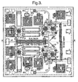
- Fig. 3 schematically shows the arrangement of the various components of the single sideband mixer Fig. 2 on a substrate.
- the two up-mixers are arranged mirror-symmetrically on both sides of a dot-dashed center line AA.
- this center line AA extends a dual balun which comprises seven parallel microstrip sections S1, S2, S3, S4, S2 ', S3', S4 '.
- a middle of these sections S1 is on one of its ends is connected to a terminal pad for the local oscillator signal LO, the other end remote from the LO terminal pad is grounded.
- this middle microstrip conductor S1 to the outside are arranged in order: a first microstrip conductor S2, S2 ', which is connected to ground at an end facing the local oscillator connection pad LO and at an opposite end via the capacitor C2 or C2' to the HEMT Q2 and Q2 ', a second microstrip S3, S3', which is connected at its local oscillator terminal pad LO end facing the corresponding end of the microstrip conductor S1 and is set at its opposite end as the microstrip conductor S1 to ground, and a third microstrip conductor S4, S4 ', which is connected at its the local oscillator pad LO end facing S1, S3, S3' and connected at its opposite end via the capacitor C1 and C1 'to the HEMT Q1 and Q1' ,
- the double balun thus simultaneously acts as a power divider which supplies the local oscillator signal LO with equal power to the two up-frequency converters on either side of the center line A-A.
Landscapes
- Engineering & Computer Science (AREA)
- Power Engineering (AREA)
- Superheterodyne Receivers (AREA)
- Transmitters (AREA)
- Control Of High-Frequency Heating Circuits (AREA)
- Channel Selection Circuits, Automatic Tuning Circuits (AREA)
- Stabilization Of Oscillater, Synchronisation, Frequency Synthesizers (AREA)
Claims (15)
- Convertisseur de fréquences vers le haut, comprenant un substrat sur lequel sont intégrés les éléments suivants :une première et une seconde entrée pour deux signaux d'entrée (IF, LO) à mélanger, le premier signal d'entrée (IF) ayant une fréquence plus basse que le second signal d'entrée (LO),un premier et un second élément de commande (Q1, Q2), comprenant chacun un raccord de commande (G) et deux raccords principaux (S, D), tels que l'écoulement de courant entre les raccords principaux peut être commandé par un signal appliqué au raccord de commande, etune sortie (HF) pour un signal mélangé engendré à partir des deux signaux d'entrée à mélanger,dans lequel les raccords de commande des deux éléments de commande (Q1, Q2) sont branchés en opposition au second signal d'entrée (LO), et les premiers raccords principaux des deux éléments de commande (Q1, Q2) sont reliés l'un à l'autre et à la sortie (HF),caractérisé par un premier circuit de symétrisation (Q3) intégré sur le substrat, qui relie l'entrée pour le premier signal d'entrée (IF) aux seconds raccords principaux des deux éléments de commande (Q1, Q2).
- Convertisseur de fréquences vers le haut selon la revendication 1, caractérisé en ce que le premier circuit de symétrisation est un troisième élément de commande (Q3), dont le raccord de commande est branché avec le premier signal d'entrée (IF), et dont les deux raccords principaux sont reliés chacun à un potentiel d'alimentation (VD1, GND) parmi deux, et à un raccord du premier ou du second élément de commande (Q1, Q2).
- Convertisseur de fréquences vers le haut selon la revendication 2, caractérisé en ce que chaque raccord principal du troisième élément de commande est relié à un second raccord principal du premier ou du second élément de commande (Q1, Q2).
- Convertisseur de fréquences vers le haut selon l'une des revendications précédentes, caractérisé en ce que les éléments de commande sont des transistors.
- Convertisseur de fréquences vers le haut selon la revendication 4, caractérisé en ce que les transistors sont des transistors HEMT.
- Convertisseur de fréquences vers le haut selon la revendication 4 ou 5, caractérisé en ce que le troisième élément de commande (Q3) fonctionne dans son domaine linéaire.
- Convertisseur de fréquences vers le haut selon l'une des revendications 4 à 6, caractérisé en ce que le premier et le second élément de commande (Q1, Q2) sont amenés en fonctionner sous une tension renforcée au voisinage de leur plage de "Pinch-Off'.
- Convertisseur de fréquences vers le haut selon la revendication 7, caractérisé en ce que le premier et le second élément de commande (Q1, Q2) sont mis sous une tension renforcée par réglage automatique du point de travail ("self bias").
- Convertisseur de fréquences vers le haut selon l'une des revendications précédentes, caractérisé par un second circuit de symétrisation (S1, S2, S3, S4 ; S1, S2, S3, S4, S2', S3', S4'), qui est relié du côté entrée à l'entrée pour le second signal d'entrée (LO) et du côté sortie aux entrées de commande du premier et du second élément de commande (Q1, Q2).
- Convertisseur de fréquences à bande latérale unique, comprenant deux convertisseurs de fréquences vers le haut selon l'une des revendications précédentes, caractérisé en ce que les sorties des deux convertisseurs de fréquence vers le haut sont raccordées à des entrées d'un coupleur de Lange (LC), une sortie de celui-ci formant une sortie du convertisseur de fréquences à bande latérale unique.
- Convertisseur de fréquences à bande latérale unique comprenant deux convertisseurs de fréquence vers le haut selon la revendication 9, caractérisé en ce que le second circuit de symétrisation (S1, S2, S3, S4, S1', S2', S3') est réalisé simultanément à la manière d'un diviseur de puissance.
- Convertisseur de fréquences à bande latérale unique selon la revendication 11, caractérisé en ce que le second circuit de symétrisation comprend un premier tronçon de conducteur central (S1), relié à une entrée de signal du convertisseur de fréquence à bande latérale unique et, des deux côtés du premier tronçon de conducteur (S1), une pluralité de seconds tronçons de conducteurs (S2, S3, S4, S2', S3', S4'), tels que les entrées de commande du premier et du second élément de commande (Q1, Q2) du premier convertisseur de fréquence vers le haut sont reliées à des seconds tronçons de conducteurs (S2, S4) sur un côté du tronçon de conducteur central, et les entrées de commande du premier et du second élément de commande (Q1', Q2') du second convertisseur de fréquences vers le haut sont reliées à des seconds tronçons de conducteurs (S2', S4') sur l'autre côté du tronçon de conducteur central (S1).
- Convertisseur de fréquences à bande latérale unique selon la revendication 12, caractérisé en ce que les tronçons de conducteurs (S1, S2, S3, S4, S2', S3', S4') sont des tronçons de conducteurs à microbandes agencés dans un plan commun.
- Convertisseur de fréquences à bande latérale unique selon la revendication 12 ou 13, caractérisé en ce que les tronçons de conducteurs (S1, S2, S3, S4, S2', S3', S4') sont parallèles et équidistants.
- Convertisseur de fréquences à bande latérale unique selon l'une des revendications 12 à 14, caractérisé en ce que le second circuit de symétrisation comprend trois tronçons de conducteurs situés les uns à côté des autres (S2, S3, S4 ; S2', S3', S4') des deux côtés du tronçon de conducteur central (S1), et en ce que, parmi les trois tronçons de conducteurs situés les uns à côté des autres, un tronçon médian respectif (S3, S3') est relié à ses deux extrémités avec le tronçon de conducteur central (S1).
Applications Claiming Priority (3)
| Application Number | Priority Date | Filing Date | Title |
|---|---|---|---|
| DE10222622 | 2002-05-17 | ||
| DE10222622A DE10222622A1 (de) | 2002-05-17 | 2002-05-17 | Aufwärts-Frequenzumsetzer |
| PCT/IB2003/002588 WO2003098794A1 (fr) | 2002-05-17 | 2003-05-19 | Convertisseur de fréquence vers le haut |
Publications (2)
| Publication Number | Publication Date |
|---|---|
| EP1509996A1 EP1509996A1 (fr) | 2005-03-02 |
| EP1509996B1 true EP1509996B1 (fr) | 2010-07-07 |
Family
ID=29285641
Family Applications (1)
| Application Number | Title | Priority Date | Filing Date |
|---|---|---|---|
| EP03732897A Expired - Lifetime EP1509996B1 (fr) | 2002-05-17 | 2003-05-19 | Convertisseur de frequence vers le haut |
Country Status (7)
| Country | Link |
|---|---|
| US (1) | US20060009173A1 (fr) |
| EP (1) | EP1509996B1 (fr) |
| CN (1) | CN1653681A (fr) |
| AT (1) | ATE473547T1 (fr) |
| AU (1) | AU2003242275A1 (fr) |
| DE (2) | DE10222622A1 (fr) |
| WO (1) | WO2003098794A1 (fr) |
Families Citing this family (2)
| Publication number | Priority date | Publication date | Assignee | Title |
|---|---|---|---|---|
| US20070173286A1 (en) * | 2005-04-04 | 2007-07-26 | Broadcom Corporation, A California Corporation | Distribution of shared local oscillation to multiple RF intefaces of a wireless device |
| US8232851B2 (en) * | 2009-03-16 | 2012-07-31 | International Business Machines Corporation | On-chip millimeter wave lange coupler |
Family Cites Families (8)
| Publication number | Priority date | Publication date | Assignee | Title |
|---|---|---|---|---|
| EP0341531A3 (fr) * | 1988-05-11 | 1991-05-15 | Licentia Patent-Verwaltungs-GmbH | Amplificateur à large bande réglable |
| US5039891A (en) * | 1989-12-20 | 1991-08-13 | Hughes Aircraft Company | Planar broadband FET balun |
| US5379457A (en) * | 1993-06-28 | 1995-01-03 | Hewlett-Packard Company | Low noise active mixer |
| JPH1056336A (ja) * | 1996-08-09 | 1998-02-24 | Mitsubishi Electric Corp | ミキサ回路 |
| US5847612A (en) * | 1997-08-01 | 1998-12-08 | Microtune, Inc. | Interference-free broadband television tuner |
| US6230001B1 (en) * | 1999-05-27 | 2001-05-08 | Rockwell Collins, Inc. | Active commutated double balanced mixer |
| JP2001111353A (ja) * | 1999-10-13 | 2001-04-20 | Mitsubishi Electric Corp | ミキサ回路 |
| FR2809552B1 (fr) * | 2000-05-25 | 2002-07-19 | Cit Alcatel | Melangeur doublement equilibre en technologie mmic |
-
2002
- 2002-05-17 DE DE10222622A patent/DE10222622A1/de not_active Withdrawn
-
2003
- 2003-05-19 EP EP03732897A patent/EP1509996B1/fr not_active Expired - Lifetime
- 2003-05-19 WO PCT/IB2003/002588 patent/WO2003098794A1/fr not_active Ceased
- 2003-05-19 AT AT03732897T patent/ATE473547T1/de active
- 2003-05-19 US US10/514,703 patent/US20060009173A1/en not_active Abandoned
- 2003-05-19 CN CN03811102.0A patent/CN1653681A/zh active Pending
- 2003-05-19 AU AU2003242275A patent/AU2003242275A1/en not_active Abandoned
- 2003-05-19 DE DE50312863T patent/DE50312863D1/de not_active Expired - Lifetime
Also Published As
| Publication number | Publication date |
|---|---|
| DE10222622A1 (de) | 2003-11-27 |
| US20060009173A1 (en) | 2006-01-12 |
| WO2003098794A1 (fr) | 2003-11-27 |
| ATE473547T1 (de) | 2010-07-15 |
| AU2003242275A1 (en) | 2003-12-02 |
| CN1653681A (zh) | 2005-08-10 |
| EP1509996A1 (fr) | 2005-03-02 |
| DE50312863D1 (de) | 2010-08-19 |
Similar Documents
| Publication | Publication Date | Title |
|---|---|---|
| DE3750667T2 (de) | Leistungsverstärker. | |
| DE3916406C2 (de) | Doppelt-symmetrischer Mischer | |
| DE4410030C2 (de) | Rauscharmer, aktiver Mischer | |
| DE3687923T2 (de) | Verteilter monolithischer mischer. | |
| DE60306606T2 (de) | Subharmonischer Gegentaktmischer | |
| DE3513659A1 (de) | Verteilter leistungsverstaerker | |
| DE3612657C2 (de) | Frequenzumsetzungseinrichtung | |
| DE102010001668A1 (de) | Leistungstransistorbaugruppe mit integrierter Sammelschiene | |
| DE69713191T2 (de) | Vorrichtung mit einem Ring-Mischer | |
| DE10100559B4 (de) | Einfachsymmetrischer Mischer | |
| DE69709882T2 (de) | Aktive miniaturumwandlung zwischen einer schlitzleitung und einem koplanaren wellenleiter | |
| DE102007019560B4 (de) | Sende- und Empfangsschaltung | |
| DE102006024458B4 (de) | Integrierte Mehrfachmischer-Schaltung | |
| DE3340566A1 (de) | Hochfrequenz-kopplungsschaltung | |
| DE60101089T2 (de) | Multifunktionelle integrierte schaltungsanordnung hoher frequenz | |
| DE3850799T2 (de) | Monolithischer Gegentakt-Einseitenbandmodulator. | |
| DE102005037877A1 (de) | Diodenmischer | |
| EP1509996A1 (fr) | Convertisseur de frequence vers le haut | |
| DE69531469T2 (de) | Quadraturmodulator für den Quasi-Mikrowellenbereich eines digitalen Übertragungssystems | |
| DE2454058B2 (de) | Ringmodulator | |
| DE2611712C3 (de) | Breitband-Wellenführungs-Mischstufe | |
| DE3324540C2 (de) | Breitbandiger Mikrowellenverstärker | |
| DE19739479C2 (de) | Hochfrequenzmischer | |
| EP0102977A1 (fr) | Dispositif de surveillance locale a radar doppler | |
| DE2525468C3 (de) | Breitbandiger Mischer für sehr hohe Frequenzen in Streifenleitungstechnik |
Legal Events
| Date | Code | Title | Description |
|---|---|---|---|
| PUAI | Public reference made under article 153(3) epc to a published international application that has entered the european phase |
Free format text: ORIGINAL CODE: 0009012 |
|
| 17P | Request for examination filed |
Effective date: 20041213 |
|
| AK | Designated contracting states |
Kind code of ref document: A1 Designated state(s): AT BE BG CH CY CZ DE DK EE ES FI FR GB GR HU IE IT LI LU MC NL PT RO SE SI SK TR |
|
| AX | Request for extension of the european patent |
Extension state: AL LT LV MK |
|
| DAX | Request for extension of the european patent (deleted) | ||
| RAP1 | Party data changed (applicant data changed or rights of an application transferred) |
Owner name: ERICSSON AB |
|
| 17Q | First examination report despatched |
Effective date: 20071122 |
|
| GRAJ | Information related to disapproval of communication of intention to grant by the applicant or resumption of examination proceedings by the epo deleted |
Free format text: ORIGINAL CODE: EPIDOSDIGR1 |
|
| GRAP | Despatch of communication of intention to grant a patent |
Free format text: ORIGINAL CODE: EPIDOSNIGR1 |
|
| GRAS | Grant fee paid |
Free format text: ORIGINAL CODE: EPIDOSNIGR3 |
|
| RAP1 | Party data changed (applicant data changed or rights of an application transferred) |
Owner name: ERICSSON AB |
|
| GRAA | (expected) grant |
Free format text: ORIGINAL CODE: 0009210 |
|
| AK | Designated contracting states |
Kind code of ref document: B1 Designated state(s): AT BE BG CH CY CZ DE DK EE ES FI FR GB GR HU IE IT LI LU MC NL PT RO SE SI SK TR |
|
| REG | Reference to a national code |
Ref country code: GB Ref legal event code: FG4D Free format text: NOT ENGLISH |
|
| REG | Reference to a national code |
Ref country code: CH Ref legal event code: EP |
|
| REG | Reference to a national code |
Ref country code: IE Ref legal event code: FG4D |
|
| REF | Corresponds to: |
Ref document number: 50312863 Country of ref document: DE Date of ref document: 20100819 Kind code of ref document: P |
|
| REG | Reference to a national code |
Ref country code: NL Ref legal event code: VDEP Effective date: 20100707 |
|
| PG25 | Lapsed in a contracting state [announced via postgrant information from national office to epo] |
Ref country code: SI Free format text: LAPSE BECAUSE OF FAILURE TO SUBMIT A TRANSLATION OF THE DESCRIPTION OR TO PAY THE FEE WITHIN THE PRESCRIBED TIME-LIMIT Effective date: 20100707 |
|
| PG25 | Lapsed in a contracting state [announced via postgrant information from national office to epo] |
Ref country code: FI Free format text: LAPSE BECAUSE OF FAILURE TO SUBMIT A TRANSLATION OF THE DESCRIPTION OR TO PAY THE FEE WITHIN THE PRESCRIBED TIME-LIMIT Effective date: 20100707 Ref country code: NL Free format text: LAPSE BECAUSE OF FAILURE TO SUBMIT A TRANSLATION OF THE DESCRIPTION OR TO PAY THE FEE WITHIN THE PRESCRIBED TIME-LIMIT Effective date: 20100707 |
|
| REG | Reference to a national code |
Ref country code: IE Ref legal event code: FD4D |
|
| PG25 | Lapsed in a contracting state [announced via postgrant information from national office to epo] |
Ref country code: BG Free format text: LAPSE BECAUSE OF FAILURE TO SUBMIT A TRANSLATION OF THE DESCRIPTION OR TO PAY THE FEE WITHIN THE PRESCRIBED TIME-LIMIT Effective date: 20101007 Ref country code: PT Free format text: LAPSE BECAUSE OF FAILURE TO SUBMIT A TRANSLATION OF THE DESCRIPTION OR TO PAY THE FEE WITHIN THE PRESCRIBED TIME-LIMIT Effective date: 20101108 Ref country code: CY Free format text: LAPSE BECAUSE OF FAILURE TO SUBMIT A TRANSLATION OF THE DESCRIPTION OR TO PAY THE FEE WITHIN THE PRESCRIBED TIME-LIMIT Effective date: 20100707 |
|
| PG25 | Lapsed in a contracting state [announced via postgrant information from national office to epo] |
Ref country code: GR Free format text: LAPSE BECAUSE OF FAILURE TO SUBMIT A TRANSLATION OF THE DESCRIPTION OR TO PAY THE FEE WITHIN THE PRESCRIBED TIME-LIMIT Effective date: 20101008 Ref country code: SE Free format text: LAPSE BECAUSE OF FAILURE TO SUBMIT A TRANSLATION OF THE DESCRIPTION OR TO PAY THE FEE WITHIN THE PRESCRIBED TIME-LIMIT Effective date: 20100707 |
|
| PG25 | Lapsed in a contracting state [announced via postgrant information from national office to epo] |
Ref country code: DK Free format text: LAPSE BECAUSE OF FAILURE TO SUBMIT A TRANSLATION OF THE DESCRIPTION OR TO PAY THE FEE WITHIN THE PRESCRIBED TIME-LIMIT Effective date: 20100707 Ref country code: IE Free format text: LAPSE BECAUSE OF FAILURE TO SUBMIT A TRANSLATION OF THE DESCRIPTION OR TO PAY THE FEE WITHIN THE PRESCRIBED TIME-LIMIT Effective date: 20100707 |
|
| PLBE | No opposition filed within time limit |
Free format text: ORIGINAL CODE: 0009261 |
|
| STAA | Information on the status of an ep patent application or granted ep patent |
Free format text: STATUS: NO OPPOSITION FILED WITHIN TIME LIMIT |
|
| PG25 | Lapsed in a contracting state [announced via postgrant information from national office to epo] |
Ref country code: SK Free format text: LAPSE BECAUSE OF FAILURE TO SUBMIT A TRANSLATION OF THE DESCRIPTION OR TO PAY THE FEE WITHIN THE PRESCRIBED TIME-LIMIT Effective date: 20100707 Ref country code: IT Free format text: LAPSE BECAUSE OF FAILURE TO SUBMIT A TRANSLATION OF THE DESCRIPTION OR TO PAY THE FEE WITHIN THE PRESCRIBED TIME-LIMIT Effective date: 20100707 Ref country code: EE Free format text: LAPSE BECAUSE OF FAILURE TO SUBMIT A TRANSLATION OF THE DESCRIPTION OR TO PAY THE FEE WITHIN THE PRESCRIBED TIME-LIMIT Effective date: 20100707 Ref country code: CZ Free format text: LAPSE BECAUSE OF FAILURE TO SUBMIT A TRANSLATION OF THE DESCRIPTION OR TO PAY THE FEE WITHIN THE PRESCRIBED TIME-LIMIT Effective date: 20100707 Ref country code: RO Free format text: LAPSE BECAUSE OF FAILURE TO SUBMIT A TRANSLATION OF THE DESCRIPTION OR TO PAY THE FEE WITHIN THE PRESCRIBED TIME-LIMIT Effective date: 20100707 |
|
| 26N | No opposition filed |
Effective date: 20110408 |
|
| PG25 | Lapsed in a contracting state [announced via postgrant information from national office to epo] |
Ref country code: ES Free format text: LAPSE BECAUSE OF FAILURE TO SUBMIT A TRANSLATION OF THE DESCRIPTION OR TO PAY THE FEE WITHIN THE PRESCRIBED TIME-LIMIT Effective date: 20101018 |
|
| REG | Reference to a national code |
Ref country code: DE Ref legal event code: R097 Ref document number: 50312863 Country of ref document: DE Effective date: 20110408 |
|
| BERE | Be: lapsed |
Owner name: ERICSSON A.B. Effective date: 20110531 |
|
| PG25 | Lapsed in a contracting state [announced via postgrant information from national office to epo] |
Ref country code: MC Free format text: LAPSE BECAUSE OF NON-PAYMENT OF DUE FEES Effective date: 20110531 |
|
| REG | Reference to a national code |
Ref country code: CH Ref legal event code: PL |
|
| PG25 | Lapsed in a contracting state [announced via postgrant information from national office to epo] |
Ref country code: CH Free format text: LAPSE BECAUSE OF NON-PAYMENT OF DUE FEES Effective date: 20110531 Ref country code: LI Free format text: LAPSE BECAUSE OF NON-PAYMENT OF DUE FEES Effective date: 20110531 |
|
| PG25 | Lapsed in a contracting state [announced via postgrant information from national office to epo] |
Ref country code: BE Free format text: LAPSE BECAUSE OF NON-PAYMENT OF DUE FEES Effective date: 20110531 |
|
| REG | Reference to a national code |
Ref country code: AT Ref legal event code: MM01 Ref document number: 473547 Country of ref document: AT Kind code of ref document: T Effective date: 20110519 |
|
| PG25 | Lapsed in a contracting state [announced via postgrant information from national office to epo] |
Ref country code: AT Free format text: LAPSE BECAUSE OF NON-PAYMENT OF DUE FEES Effective date: 20110519 |
|
| PG25 | Lapsed in a contracting state [announced via postgrant information from national office to epo] |
Ref country code: LU Free format text: LAPSE BECAUSE OF NON-PAYMENT OF DUE FEES Effective date: 20110519 |
|
| PG25 | Lapsed in a contracting state [announced via postgrant information from national office to epo] |
Ref country code: TR Free format text: LAPSE BECAUSE OF FAILURE TO SUBMIT A TRANSLATION OF THE DESCRIPTION OR TO PAY THE FEE WITHIN THE PRESCRIBED TIME-LIMIT Effective date: 20100707 |
|
| PG25 | Lapsed in a contracting state [announced via postgrant information from national office to epo] |
Ref country code: HU Free format text: LAPSE BECAUSE OF FAILURE TO SUBMIT A TRANSLATION OF THE DESCRIPTION OR TO PAY THE FEE WITHIN THE PRESCRIBED TIME-LIMIT Effective date: 20100707 |
|
| REG | Reference to a national code |
Ref country code: FR Ref legal event code: PLFP Year of fee payment: 14 |
|
| REG | Reference to a national code |
Ref country code: FR Ref legal event code: PLFP Year of fee payment: 15 |
|
| REG | Reference to a national code |
Ref country code: FR Ref legal event code: PLFP Year of fee payment: 16 |
|
| PGFP | Annual fee paid to national office [announced via postgrant information from national office to epo] |
Ref country code: DE Payment date: 20180529 Year of fee payment: 16 |
|
| PGFP | Annual fee paid to national office [announced via postgrant information from national office to epo] |
Ref country code: FR Payment date: 20180525 Year of fee payment: 16 |
|
| PGFP | Annual fee paid to national office [announced via postgrant information from national office to epo] |
Ref country code: GB Payment date: 20180529 Year of fee payment: 16 |
|
| REG | Reference to a national code |
Ref country code: DE Ref legal event code: R119 Ref document number: 50312863 Country of ref document: DE |
|
| GBPC | Gb: european patent ceased through non-payment of renewal fee |
Effective date: 20190519 |
|
| PG25 | Lapsed in a contracting state [announced via postgrant information from national office to epo] |
Ref country code: GB Free format text: LAPSE BECAUSE OF NON-PAYMENT OF DUE FEES Effective date: 20190519 Ref country code: DE Free format text: LAPSE BECAUSE OF NON-PAYMENT OF DUE FEES Effective date: 20191203 |
|
| PG25 | Lapsed in a contracting state [announced via postgrant information from national office to epo] |
Ref country code: FR Free format text: LAPSE BECAUSE OF NON-PAYMENT OF DUE FEES Effective date: 20190531 |